EP2613367A2 - Verfahren zur Herstellung einer LED-Vorrichtung - Google Patents
Verfahren zur Herstellung einer LED-Vorrichtung Download PDFInfo
- Publication number
- EP2613367A2 EP2613367A2 EP12196619.6A EP12196619A EP2613367A2 EP 2613367 A2 EP2613367 A2 EP 2613367A2 EP 12196619 A EP12196619 A EP 12196619A EP 2613367 A2 EP2613367 A2 EP 2613367A2
- Authority
- EP
- European Patent Office
- Prior art keywords
- features
- regular pattern
- layer
- deviation
- pattern
- Prior art date
- Legal status (The legal status is an assumption and is not a legal conclusion. Google has not performed a legal analysis and makes no representation as to the accuracy of the status listed.)
- Withdrawn
Links
- 238000004519 manufacturing process Methods 0.000 title claims abstract description 9
- 238000000034 method Methods 0.000 claims abstract description 27
- 238000000605 extraction Methods 0.000 claims abstract description 9
- 230000002708 enhancing effect Effects 0.000 claims abstract description 5
- 238000009826 distribution Methods 0.000 claims description 9
- 238000001459 lithography Methods 0.000 claims description 6
- 229910002601 GaN Inorganic materials 0.000 description 6
- 239000000758 substrate Substances 0.000 description 5
- QNRATNLHPGXHMA-XZHTYLCXSA-N (r)-(6-ethoxyquinolin-4-yl)-[(2s,4s,5r)-5-ethyl-1-azabicyclo[2.2.2]octan-2-yl]methanol;hydrochloride Chemical compound Cl.C([C@H]([C@H](C1)CC)C2)CN1[C@@H]2[C@H](O)C1=CC=NC2=CC=C(OCC)C=C21 QNRATNLHPGXHMA-XZHTYLCXSA-N 0.000 description 3
- 238000001312 dry etching Methods 0.000 description 3
- VYPSYNLAJGMNEJ-UHFFFAOYSA-N Silicium dioxide Chemical compound O=[Si]=O VYPSYNLAJGMNEJ-UHFFFAOYSA-N 0.000 description 2
- PPBRXRYQALVLMV-UHFFFAOYSA-N Styrene Chemical compound C=CC1=CC=CC=C1 PPBRXRYQALVLMV-UHFFFAOYSA-N 0.000 description 2
- 230000007423 decrease Effects 0.000 description 2
- 238000000151 deposition Methods 0.000 description 2
- 238000005530 etching Methods 0.000 description 2
- 229910052710 silicon Inorganic materials 0.000 description 2
- ZAMOUSCENKQFHK-UHFFFAOYSA-N Chlorine atom Chemical compound [Cl] ZAMOUSCENKQFHK-UHFFFAOYSA-N 0.000 description 1
- JMASRVWKEDWRBT-UHFFFAOYSA-N Gallium nitride Chemical compound [Ga]#N JMASRVWKEDWRBT-UHFFFAOYSA-N 0.000 description 1
- 208000012868 Overgrowth Diseases 0.000 description 1
- 239000004793 Polystyrene Substances 0.000 description 1
- 229910052581 Si3N4 Inorganic materials 0.000 description 1
- 229910052801 chlorine Inorganic materials 0.000 description 1
- 239000000460 chlorine Substances 0.000 description 1
- 229910052681 coesite Inorganic materials 0.000 description 1
- 150000001875 compounds Chemical class 0.000 description 1
- 229910052906 cristobalite Inorganic materials 0.000 description 1
- 230000001419 dependent effect Effects 0.000 description 1
- 230000008021 deposition Effects 0.000 description 1
- 230000000694 effects Effects 0.000 description 1
- 238000005516 engineering process Methods 0.000 description 1
- 239000000463 material Substances 0.000 description 1
- 238000004377 microelectronic Methods 0.000 description 1
- 239000004038 photonic crystal Substances 0.000 description 1
- 229920002223 polystyrene Polymers 0.000 description 1
- 239000004065 semiconductor Substances 0.000 description 1
- 239000010703 silicon Substances 0.000 description 1
- 239000000377 silicon dioxide Substances 0.000 description 1
- 229910052682 stishovite Inorganic materials 0.000 description 1
- 229910052905 tridymite Inorganic materials 0.000 description 1
- 238000009827 uniform distribution Methods 0.000 description 1
- 238000001039 wet etching Methods 0.000 description 1
Images


Classifications
-
- G—PHYSICS
- G03—PHOTOGRAPHY; CINEMATOGRAPHY; ANALOGOUS TECHNIQUES USING WAVES OTHER THAN OPTICAL WAVES; ELECTROGRAPHY; HOLOGRAPHY
- G03F—PHOTOMECHANICAL PRODUCTION OF TEXTURED OR PATTERNED SURFACES, e.g. FOR PRINTING, FOR PROCESSING OF SEMICONDUCTOR DEVICES; MATERIALS THEREFOR; ORIGINALS THEREFOR; APPARATUS SPECIALLY ADAPTED THEREFOR
- G03F7/00—Photomechanical, e.g. photolithographic, production of textured or patterned surfaces, e.g. printing surfaces; Materials therefor, e.g. comprising photoresists; Apparatus specially adapted therefor
- G03F7/0005—Production of optical devices or components in so far as characterised by the lithographic processes or materials used therefor
-
- H—ELECTRICITY
- H10—SEMICONDUCTOR DEVICES; ELECTRIC SOLID-STATE DEVICES NOT OTHERWISE PROVIDED FOR
- H10H—INORGANIC LIGHT-EMITTING SEMICONDUCTOR DEVICES HAVING POTENTIAL BARRIERS
- H10H20/00—Individual inorganic light-emitting semiconductor devices having potential barriers, e.g. light-emitting diodes [LED]
- H10H20/80—Constructional details
- H10H20/81—Bodies
- H10H20/819—Bodies characterised by their shape, e.g. curved or truncated substrates
- H10H20/82—Roughened surfaces, e.g. at the interface between epitaxial layers
Definitions
- the present invention is related to the field of semiconductor processing, in particular to the field of LED devices, such as GaNLEDs (Gallium Nitride LEDs).
- LED devices such as GaNLEDs (Gallium Nitride LEDs).
- GaNLED technology has become important in the development and production of various applications, such as notebook and TV backlighting and general lighting. It is known that surface texturization of the GaN layer improves the light extraction efficiency of the LED (extract more light from the device). Texturizing of GaN can be done with a suitable wet etching solution such as KOH or by dry etching of the GaN layer. The latter technique involves the use of a mask that defines a pattern of texturing features on the surface. Conventional I-line lithography and chlorine based dry etching may be used to produce said features on the surface according to the pattern defined by the mask. Another option is to provide a layer of polystyrene spheres on the surface, and using said spheres as a mask for the dry etch. These techniques are illustrated for example in EP0977277 .
- the pattern of features transferred to the textured surface is preferably not a regular pattern, i.e. the size of the features and the distance between neighbouring features is not constant over the surface.
- Regular patterns tend to capture too much light emitted by the LED's light emitting layer through repeated reflection of the light along the same reflection angles. More randomness enhances the variability of the reflection angles and therefore the amount of light emerging from the LED device. Random patterned masks and lithography is therefore a preferred option, or the solution of the styrene spheres, which creates a fully random pattern over a large surface.
- the invention is related to a method as disclosed in the appended claims.
- the invention is thus related to a method for producing a LED device, comprising a stack of layers comprising a light producing layer said light producing layer not being the top or bottom layer of said stack, the method comprising a texturization step, wherein a layer at the top or bottom of the stack is subjected to a texturization aimed at enhancing the light extraction efficiency of the LED, wherein said texturization comprises the step of producing on said top or bottom surface a plurality of surface features, said surface features being arranged according to a pattern defined by starting from a regular pattern of features and subjecting each feature of said regular pattern to a deviation from the location in the regular pattern, said deviation being in a random direction and/or having a random amplitude.
- the amplitude of said deviation is not higher than the pitch of the features of said regular pattern.
- the amplitude of said deviation is such that essentially no surface features are mutually overlapping in said pattern.
- the amplitude of said deviation is not higher than half of the pitch of the features of said regular pattern.
- the amplitude of said deviation may be configured to be according to a predefined statistical distribution, such as a uniform or a Gaussian distribution.
- the pitch of the features of said regular pattern is between 0.2micron and 2micron.
- said surface features are shaped as cone or pyramid-shaped pillars with a flat top surface, flat areas between said pillars, the pillars having slanted side surfaces.
- said side surface are inclined at an angle between 25° and 45°, with respect to the plane of the texturized surface, preferably between 25° and 30°.
- the width of said top surface of each feature is configured so that the emission cone emitted from the point of the light-producing layer situated underneath the mid point of said top surface and received by said top surface, essentially corresponds to the escape cone of light emitted by the light producing layer through a non-texturized surface having the same thickness as the top surface.
- the amplitude of the deviation is preferably not higher than one fourth of the pitch of the features of said regular pattern.
- said texturization comprises a lithography step wherein a mask is used, said mask having openings arranged according to said non-regular pattern.
- the invention is equally related to a method for producing a LED device, comprising a stack of layers comprising a light producing layer said light producing layer not being the top or bottom layer of said stack, the method comprising a texturization step, wherein a layer at the top or bottom of the stack is subjected to a texturization aimed at enhancing the light extraction efficiency of the LED, wherein said texturization comprises the step of producing on said top or bottom surface a plurality of surface features, said surface features being arranged according to a pattern defined by starting from a regular pattern of features of equal size and shape and subjecting one or more dimensions of each feature of said regular pattern to a random deviation from the dimensions of said equal-sized.
- Figure 1 illustrates the problem of light becoming trapped in a LED device provided with a non-texturized surface.
- Figure 2 illustrates the improvement in terms of light extraction efficiency obtained through texturization of the surface.
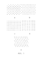
- Figure 3 shows examples of regular patterns of surface features.
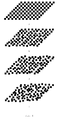
- Figure 4 illustrates a rhombic pattern of features provided with various degrees of a 'jitter' according to the invention.
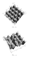
- Figure 5 gives an example of a hexagonal pattern before and after application of a 'jitter' to the pattern.
- Figure 6 illustrates a preferred feature geometry especially suitable in combination with the method according to the invention.
- the invention is related to a method for producing a LED comprising a stack of layers, said stack comprising a light producing layer (such as one or more quantum wells) in the interior of the stack, i.e. not at the top or bottom of the stack.
- Figure 1 illustrates in a very schematic way the basic structure of such a LED device, including a mirror surface 1, the LED stack 2, with the light-producing layer 3.
- a top layer that is not texturized as in figure 1 , light emitted in directions outside the so-called 'escape cone' 5 is for the most part trapped inside the layer due to the repeated reflections of the emitted beams 6.
- the texturization is done by producing a plurality of surface features on the surface, for example microscopic pillars or depressions in the surface, said surface features being arranged according to a non-regular pattern defined by starting from a regular pattern of features and subjecting each feature of said regular pattern to a deviation from the location in the regular pattern, said deviation being in a random direction and/or having a random amplitude.
- a regular pattern is a pattern wherein each feature has the same pre-defined relative position with respect to adjacent features. The random deviation is hereafter referred to as a 'jitter' imposed on the regular pattern.
- the regular pattern may be for example rhombic (checkerboard pattern), hexagonal, square, rectangular or oblique, as illustrated in figure 3a to 3e respectively, but any other regular pattern may be chosen.
- the amplitude of the jitter (how much the feature deviates from the regular position) may have a fixed value applied in a random direction around the regular feature positions, or it may itself be random (combined with a random or non-random direction of the jitter). It may be random but confined within a predefined interval of deviations, for example between zero and a maximum or between a minimum and maximum deviation.
- the direction of the jitter is random and the amplitude of the jitter is random but configured to have a predefined statistical distribution, for example a uniform or a Gaussian distribution, around the regular position of the features, and deviating from the regular position in a random direction. Variance values of such distributions may be chosen in order to obtain more or less spread of the features over the surface 4 with respect to the regular pattern positions.
- Figure 4a illustrates a 50% rhombic pattern (i.e. the surface features cover 50% of the surface before the jitter is applied).
- Figures 4b to 4d illustrate the same pattern, with a uniformly distributed jitter applied to it with increasing maximum amplitude.
- Figure 5a shows an example of a hexagonal regular pattern of pillar-like structures.
- Figure 5b shows a jittered pattern (uniform distribution) according to the invention and based on the pattern of Figure 5a , with the pillars deviating from their regular positions.
- the scales indicated in these drawings are in microns.
- the 'jittered' pattern may be applied to the surface of the LED, e.g. to a GaN-based layer stack comprising multiple quantum wells, by a known technique, preferably by a dry etch involving a mask and standard lithography, wherein the pattern is transferred to a resist layer by illuminating the resist through said mask, developing and removing the illuminated resist and etching openings in the stack's top layer as defined by the resist openings, before finally removing the resist.
- the result is a surface provided with pillar-like features.
- the resist portions that are not illuminated are developed and removed, leaving islands of resist, followed by the dry etch which creates inversed pillar-shaped depressions in the surface, thereby texturizing the surface.
- a SiO 2 mask (or other materials such as Si 3 N 4 , SiC, silicon-oxynitrides or compounds of Si, O, C and N) may be produced on the device wafer surface, said mask comprising a pattern of openings, said pattern being defined as described above (i.e.
- the LED stack is then deposited first on the protrusions defined by said mask, followed by overgrowth. After the transfer of the device to the carrier and removal of the device wafer, the pattern appears on the top surface of the LED.
- the mask is either removed before LED stack deposition or kept until the substrate is transferred, or even thereafter.
- This embodiment of the method of the invention may be called 'indirect texturization' of the LED layer, whereas dry etching the LED layer directly with the help of a mask is 'direct texturization'.
- the indirect method may be used to pattern the bottom surface of the stack 2.
- the jittered pattern of the invention offers the advantage of a better control and repeatability of the randomness of the pattern, compared to existing methods, while maintaining the advantages of a fully random pattern, i.e. an improvement in terms of the light extraction efficiency of the LED device.
- the pitch of the features in the regular pattern used to obtain the textured surface is between 0.2 and 2micron.
- the pitch is defined as the average distance between corresponding points of two neighbouring features, e.g. between the tops of two neighbouring pyramidal pillars.
- the jitter offers an additional advantage, namely the reduction of directionality of the emitted light.
- Regular feature patterns in the pitch-range of about 0.2 to 0.5micron are known as 'photonic lattices' or 'photonic crystals'. These structures are known to emit directional light, i.e. light directed according to a limited angle around a plurality of predefined directions.
- Such directionality is a desired feature in some cases, such as in certain types of projectors, but for LEDs it is preferred to have a more diffuse emission of light.
- the optimal average amplitude of the jitter may differ depending on the shape, size and pitch of the features in the regular pattern on which the jittered pattern is based. It is not preferred to have a too large deviation from the regular position, as this may give rise to overlapping features and larger open spaces between features, which deteriorates the scattering effect of the texturization.
- the amplitude of the jitter is such that essentially no surface features are overlapping in the pattern resulting from adding the jitter to the regular pattern.
- the amplitude of the jitter is not higher than the pitch of the regular pattern to which the jitter is added, more preferably not higher than half of the pitch of said regular pattern.
- FIG. 6a A preferred embodiment of pillar-shaped features that is especially suitable for the method of the invention is shown in figure 6a .
- the dimensions that are shown are meant to give a realistic example, and are not limiting the scope of the invention.
- the figure shows the pillars 10 in a regular pattern with a pitch of 4micron, for example a square or rectangular pattern, i.e. before applying a jitter to the pattern.
- Each pillar is shaped as a pyramid or cone with a flat top surface 11 and a flat area 12 between two neighbouring features.
- the sides of the features are defined by sloping surfaces 13.
- the width of the top surfaces 11 of the features is preferably chosen in relation to the position of the light emitting layer 3 and the thickness T of the layer (indicated in figure 6a ).
- One way of doing this is by configuring the pillars so that the emission cone 14 received by the flat top surface 11 and emitted from the point 15 situated underneath the middle of said flat surface 11, corresponds essentially with the escape cone as described above, for a non-texturized surface of the same thickness T as the flat surface portions 11. In that way, at least for light emitted from these middle points 15, there is no light trapped in the layer.
- the angle of the slopes 13 with respect to the vertical is preferably about 25° to 30°, in order to scatter a maximum of light.
- the flat areas 12 in between the pillars 10 should be as small as possible in order to minimize the amount of light trapped between the parallel surfaces of the mirror and of these flat areas (see beam 16).
- a jitter preferably a uniformly distributed jitter
- a higher jitter preferably uniformly distributed
- a higher jitter of maximum up to half the pitch (+-2micron) is preferred for reducing the average top surface areas 11.
- a possible jitter range 17 applied to the pattern of figure 6a is schematically illustrated in figure 6b .
- the dimensions of the features may be subjected to a jitter, i.e. starting from a regular pattern of equal-sized features, one or more dimensions (height, width,...) of the features is enlarged or reduced in a random way.
- the amplitude of the deviation from the regular dimensions are distributed according to a predefined statistical distribution (uniform, Gaussian, etc..).
- the description of a layer being deposited or produced 'on' another layer or substrate includes the options of
Landscapes
- Physics & Mathematics (AREA)
- General Physics & Mathematics (AREA)
- Led Devices (AREA)
- Led Device Packages (AREA)
Applications Claiming Priority (1)
| Application Number | Priority Date | Filing Date | Title |
|---|---|---|---|
| US201261584143P | 2012-01-06 | 2012-01-06 |
Publications (2)
| Publication Number | Publication Date |
|---|---|
| EP2613367A2 true EP2613367A2 (de) | 2013-07-10 |
| EP2613367A3 EP2613367A3 (de) | 2013-09-04 |
Family
ID=47605314
Family Applications (1)
| Application Number | Title | Priority Date | Filing Date |
|---|---|---|---|
| EP12196619.6A Withdrawn EP2613367A3 (de) | 2012-01-06 | 2012-12-12 | Verfahren zur Herstellung einer LED-Vorrichtung |
Country Status (3)
| Country | Link |
|---|---|
| US (1) | US8900801B2 (de) |
| EP (1) | EP2613367A3 (de) |
| JP (1) | JP2013143566A (de) |
Families Citing this family (1)
| Publication number | Priority date | Publication date | Assignee | Title |
|---|---|---|---|---|
| US6727818B1 (en) | 1999-10-29 | 2004-04-27 | Hill-Rom Services, Inc. | Hygiene monitoring system |
Citations (1)
| Publication number | Priority date | Publication date | Assignee | Title |
|---|---|---|---|---|
| EP0977277A1 (de) | 1998-07-28 | 2000-02-02 | Interuniversitair Microelektronica Centrum Vzw | Strahlenemittierende Vorrichtungen mit hohem Wirkungsgrad und Herstellungsverfahren |
Family Cites Families (18)
| Publication number | Priority date | Publication date | Assignee | Title |
|---|---|---|---|---|
| DE2946235C3 (de) | 1979-11-16 | 1982-04-08 | Dr. Johannes Heidenhain Gmbh, 8225 Traunreut | Verfahren zur Erzeugung einer Belichtungsmaske zur Herstellung von mattstreuenden Strukturen neben opaken und/oder transparenten Strukturen |
| US5510156A (en) | 1994-08-23 | 1996-04-23 | Analog Devices, Inc. | Micromechanical structure with textured surface and method for making same |
| US6504180B1 (en) | 1998-07-28 | 2003-01-07 | Imec Vzw And Vrije Universiteit | Method of manufacturing surface textured high-efficiency radiating devices and devices obtained therefrom |
| US6350388B1 (en) | 1999-08-19 | 2002-02-26 | Micron Technology, Inc. | Method for patterning high density field emitter tips |
| JP4363012B2 (ja) | 2002-08-30 | 2009-11-11 | ソニー株式会社 | 半導体装置の製造方法 |
| JP2004272195A (ja) | 2003-02-20 | 2004-09-30 | Seiko Epson Corp | ランダムパターンの作成方法、マスクの製造方法、電気光学装置の製造方法、及びランダムパターンの作成プログラム |
| US8604497B2 (en) * | 2003-09-26 | 2013-12-10 | Osram Opto Semiconductors Gmbh | Radiation-emitting thin-film semiconductor chip |
| US7450311B2 (en) * | 2003-12-12 | 2008-11-11 | Luminus Devices, Inc. | Optical display systems and methods |
| US7534633B2 (en) * | 2004-07-02 | 2009-05-19 | Cree, Inc. | LED with substrate modifications for enhanced light extraction and method of making same |
| US7212345B2 (en) | 2004-09-13 | 2007-05-01 | Eastman Kodak Company | Randomized patterns of individual optical elements |
| US7670726B2 (en) | 2006-07-20 | 2010-03-02 | Zhijian Lu | Optical diffusers, photomasks and their methods of fabrication |
| JP2008185970A (ja) | 2007-01-31 | 2008-08-14 | Renesas Technology Corp | パターンの形成方法、電子デバイスの製造方法および電子デバイス |
| JP5311326B2 (ja) | 2008-02-18 | 2013-10-09 | ルネサスエレクトロニクス株式会社 | フォトマスク、パターンの形成方法および電子デバイスの製造方法 |
| DE102008045028B4 (de) * | 2008-08-29 | 2023-03-16 | OSRAM Opto Semiconductors Gesellschaft mit beschränkter Haftung | Optoelektronischer Halbleiterchip |
| DE102008062932A1 (de) * | 2008-12-23 | 2010-06-24 | Osram Opto Semiconductors Gmbh | Optoelektronischer Halbleiterchip und Verfahren zur Herstellung eines optoelektronischen Halbleiterchips |
| TW201121100A (en) * | 2009-06-09 | 2011-06-16 | Sinmat Inc | High light extraction efficiency solid state light sources |
| CN102054279A (zh) | 2009-11-02 | 2011-05-11 | 住友化学株式会社 | 随机图案的生成方法 |
| EP2597687B1 (de) * | 2011-11-23 | 2016-02-03 | Imec | Verfahren zur Erzeugung einer GaN LED-Vorrichtung |
-
2012
- 2012-12-12 EP EP12196619.6A patent/EP2613367A3/de not_active Withdrawn
- 2012-12-14 JP JP2012273616A patent/JP2013143566A/ja active Pending
- 2012-12-14 US US13/715,763 patent/US8900801B2/en not_active Expired - Fee Related
Patent Citations (1)
| Publication number | Priority date | Publication date | Assignee | Title |
|---|---|---|---|---|
| EP0977277A1 (de) | 1998-07-28 | 2000-02-02 | Interuniversitair Microelektronica Centrum Vzw | Strahlenemittierende Vorrichtungen mit hohem Wirkungsgrad und Herstellungsverfahren |
Non-Patent Citations (1)
| Title |
|---|
| PHAM ET AL.: "Substrate Transfer for GaN based LEDs grown in Silicon", IMAPS 44 INTERNATIONAL SYMPOSIUM ON MICROELECTRONICS, OCT 9-13, 2011, LONG BEACH CALIFORNIA, 9 October 2011 (2011-10-09), pages 130 - 135 |
Also Published As
| Publication number | Publication date |
|---|---|
| EP2613367A3 (de) | 2013-09-04 |
| US20130177856A1 (en) | 2013-07-11 |
| JP2013143566A (ja) | 2013-07-22 |
| US8900801B2 (en) | 2014-12-02 |
Similar Documents
| Publication | Publication Date | Title |
|---|---|---|
| TWI531086B (zh) | An optical substrate, a semiconductor light-emitting element, and a semiconductor light-emitting element | |
| JP5196403B2 (ja) | サファイア基板の製造方法、および半導体装置 | |
| TWI543395B (zh) | 圖案化光電基板及其製作方法 | |
| JP5255082B2 (ja) | 発光ダイオード | |
| JP5054366B2 (ja) | ナノ構造物が形成された基板の製造方法及び発光素子並びにその製造方法 | |
| CN102769082B (zh) | 图形化衬底及其形成方法及用于制作所述衬底的掩膜版 | |
| JP2007273746A (ja) | 固体表面の微細加工方法および発光素子 | |
| KR20150052205A (ko) | 광학 기판, 반도체 발광 소자 및 그의 제조 방법 | |
| JP2009231689A (ja) | 半導体発光素子及びその製造方法 | |
| KR20080018137A (ko) | 마이크로 및 나노 구조체의 제조방법 | |
| KR20060121422A (ko) | 광 추출용 나노 로드를 갖는 발광 소자 및 그의 제조방법 | |
| KR102120264B1 (ko) | 발광 디바이스 및 발광 디바이스를 제조하기 위한 방법 | |
| TW201349565A (zh) | 具有圖形化界面之發光元件及其製造方法 | |
| US20090026471A1 (en) | Light-scattering structure, light emitting device comprising the same and method of forming the same | |
| CN202513200U (zh) | 图形化衬底及用于制作所述衬底的掩膜板 | |
| US20070085098A1 (en) | Patterned devices and related methods | |
| CN103247733A (zh) | 发光半导体的图案化基材及其制造方法与发光半导体装置 | |
| US7388233B2 (en) | Patchwork patterned devices and related methods | |
| US7391059B2 (en) | Isotropic collimation devices and related methods | |
| US8900801B2 (en) | Method for producing a LED device | |
| KR20120077534A (ko) | 나노 구조체를 이용한 발광다이오드 제조 방법과 이에 의해 제조된 발광다이오드 | |
| US7348603B2 (en) | Anisotropic collimation devices and related methods | |
| CN202633368U (zh) | 图形化衬底及用于制作所述衬底的掩膜版 | |
| US20150171279A1 (en) | Epitaxial substrate, method thereof, and light emitting diode | |
| CN111066160B (zh) | 用于制造光电子半导体芯片的方法和光电子半导体芯片 |
Legal Events
| Date | Code | Title | Description |
|---|---|---|---|
| PUAI | Public reference made under article 153(3) epc to a published international application that has entered the european phase |
Free format text: ORIGINAL CODE: 0009012 |
|
| AK | Designated contracting states |
Kind code of ref document: A2 Designated state(s): AL AT BE BG CH CY CZ DE DK EE ES FI FR GB GR HR HU IE IS IT LI LT LU LV MC MK MT NL NO PL PT RO RS SE SI SK SM TR |
|
| AX | Request for extension of the european patent |
Extension state: BA ME |
|
| PUAL | Search report despatched |
Free format text: ORIGINAL CODE: 0009013 |
|
| AK | Designated contracting states |
Kind code of ref document: A3 Designated state(s): AL AT BE BG CH CY CZ DE DK EE ES FI FR GB GR HR HU IE IS IT LI LT LU LV MC MK MT NL NO PL PT RO RS SE SI SK SM TR |
|
| AX | Request for extension of the european patent |
Extension state: BA ME |
|
| RIC1 | Information provided on ipc code assigned before grant |
Ipc: H01L 33/22 20100101AFI20130731BHEP |
|
| STAA | Information on the status of an ep patent application or granted ep patent |
Free format text: STATUS: THE APPLICATION IS DEEMED TO BE WITHDRAWN |
|
| 18D | Application deemed to be withdrawn |
Effective date: 20140305 |