EP2615437A2 - Thermographie à haute résolution - Google Patents
Thermographie à haute résolution Download PDFInfo
- Publication number
- EP2615437A2 EP2615437A2 EP13150732.9A EP13150732A EP2615437A2 EP 2615437 A2 EP2615437 A2 EP 2615437A2 EP 13150732 A EP13150732 A EP 13150732A EP 2615437 A2 EP2615437 A2 EP 2615437A2
- Authority
- EP
- European Patent Office
- Prior art keywords
- planar surface
- orifices
- sensitive devices
- dimension
- chip
- Prior art date
- Legal status (The legal status is an assumption and is not a legal conclusion. Google has not performed a legal analysis and makes no representation as to the accuracy of the status listed.)
- Withdrawn
Links
Images


Classifications
-
- G—PHYSICS
- G01—MEASURING; TESTING
- G01J—MEASUREMENT OF INTENSITY, VELOCITY, SPECTRAL CONTENT, POLARISATION, PHASE OR PULSE CHARACTERISTICS OF INFRARED, VISIBLE OR ULTRAVIOLET LIGHT; COLORIMETRY; RADIATION PYROMETRY
- G01J5/00—Radiation pyrometry, e.g. infrared or optical thermometry
- G01J5/0003—Radiation pyrometry, e.g. infrared or optical thermometry for sensing the radiant heat transfer of samples, e.g. emittance meter
- G01J5/0007—Radiation pyrometry, e.g. infrared or optical thermometry for sensing the radiant heat transfer of samples, e.g. emittance meter of wafers or semiconductor substrates, e.g. using Rapid Thermal Processing
-
- H—ELECTRICITY
- H10—SEMICONDUCTOR DEVICES; ELECTRIC SOLID-STATE DEVICES NOT OTHERWISE PROVIDED FOR
- H10F—INORGANIC SEMICONDUCTOR DEVICES SENSITIVE TO INFRARED RADIATION, LIGHT, ELECTROMAGNETIC RADIATION OF SHORTER WAVELENGTH OR CORPUSCULAR RADIATION
- H10F39/00—Integrated devices, or assemblies of multiple devices, comprising at least one element covered by group H10F30/00, e.g. radiation detectors comprising photodiode arrays
- H10F39/10—Integrated devices
- H10F39/12—Image sensors
-
- G—PHYSICS
- G01—MEASURING; TESTING
- G01J—MEASUREMENT OF INTENSITY, VELOCITY, SPECTRAL CONTENT, POLARISATION, PHASE OR PULSE CHARACTERISTICS OF INFRARED, VISIBLE OR ULTRAVIOLET LIGHT; COLORIMETRY; RADIATION PYROMETRY
- G01J5/00—Radiation pyrometry, e.g. infrared or optical thermometry
- G01J5/02—Constructional details
- G01J5/06—Arrangements for eliminating effects of disturbing radiation; Arrangements for compensating changes in sensitivity
-
- G—PHYSICS
- G01—MEASURING; TESTING
- G01J—MEASUREMENT OF INTENSITY, VELOCITY, SPECTRAL CONTENT, POLARISATION, PHASE OR PULSE CHARACTERISTICS OF INFRARED, VISIBLE OR ULTRAVIOLET LIGHT; COLORIMETRY; RADIATION PYROMETRY
- G01J5/00—Radiation pyrometry, e.g. infrared or optical thermometry
- G01J5/02—Constructional details
- G01J5/07—Arrangements for adjusting the solid angle of collected radiation, e.g. adjusting or orienting field of view, tracking position or encoding angular position
-
- G—PHYSICS
- G01—MEASURING; TESTING
- G01J—MEASUREMENT OF INTENSITY, VELOCITY, SPECTRAL CONTENT, POLARISATION, PHASE OR PULSE CHARACTERISTICS OF INFRARED, VISIBLE OR ULTRAVIOLET LIGHT; COLORIMETRY; RADIATION PYROMETRY
- G01J5/00—Radiation pyrometry, e.g. infrared or optical thermometry
- G01J5/02—Constructional details
- G01J5/08—Optical arrangements
- G01J5/0831—Masks; Aperture plates; Spatial light modulators
-
- G—PHYSICS
- G01—MEASURING; TESTING
- G01J—MEASUREMENT OF INTENSITY, VELOCITY, SPECTRAL CONTENT, POLARISATION, PHASE OR PULSE CHARACTERISTICS OF INFRARED, VISIBLE OR ULTRAVIOLET LIGHT; COLORIMETRY; RADIATION PYROMETRY
- G01J5/00—Radiation pyrometry, e.g. infrared or optical thermometry
- G01J5/48—Thermography; Techniques using wholly visual means
-
- H—ELECTRICITY
- H10—SEMICONDUCTOR DEVICES; ELECTRIC SOLID-STATE DEVICES NOT OTHERWISE PROVIDED FOR
- H10F—INORGANIC SEMICONDUCTOR DEVICES SENSITIVE TO INFRARED RADIATION, LIGHT, ELECTROMAGNETIC RADIATION OF SHORTER WAVELENGTH OR CORPUSCULAR RADIATION
- H10F77/00—Constructional details of devices covered by this subclass
- H10F77/40—Optical elements or arrangements
- H10F77/413—Optical elements or arrangements directly associated or integrated with the devices, e.g. back reflectors
-
- G—PHYSICS
- G01—MEASURING; TESTING
- G01J—MEASUREMENT OF INTENSITY, VELOCITY, SPECTRAL CONTENT, POLARISATION, PHASE OR PULSE CHARACTERISTICS OF INFRARED, VISIBLE OR ULTRAVIOLET LIGHT; COLORIMETRY; RADIATION PYROMETRY
- G01J5/00—Radiation pyrometry, e.g. infrared or optical thermometry
- G01J2005/0077—Imaging
Definitions
- the present invention relates to temperature sensing, and more specifically, to sensing high resolution thermography.
- thermographic imaging device includes a focal array portion including a planar arrangement of a plurality of light sensitive devices, and an aperture portion including a facing planar surface, an opposing planar surface, and an arrangement of a plurality of orifices that are communicative with the facing planar surface and the opposing planar surface, each infrared sensitive device of the plurality of infrared arranged in alignment with a corresponding orifice of the plurality of orifices.
- FIG. 2 illustrates a perspective view of a portion of thermography system.
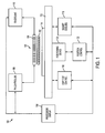
- FIG. 1 illustrates a block diagram of an exemplary embodiment of a thermography system 100.
- the system 100 includes an imaging device 101 that includes a near field aperture array (NFAA) portion 102 and a focal plane detector array 104 (each described in further detail below).
- the focal array 104 includes a planar array of a plurality of electromagnetic (e.g., IR) sensitive devices such as, for example, IR sensitive pixels that are operative to convert IR photons into electrons.
- the NFAA portion 102 includes a plurality of orifices that correspond to each of the IR sensitive devices.
- the focal array 104 is communicatively connected to a focal array controller portion 106 that is operative to receive the electrons output by the focal array 104.
- the focal array controller portion 106 may be communicatively connected to a processor and/or display device 108 that is operative to receive data from the focal array 104 controller and output the data to the display device 108.
- the focal array 104 may be connected to a focal array cooler portion 110 that is operative to cool the focal array 104.
- the system 100 includes a test socket 112 that is operative to secure a semiconductor device or chip 114 in a desired position by, for example, engaging pins of the chip with conductive contacts.
- the conductive contacts of the chip test socket (socket) 112 are communicatively connected to a chip test control portion 116 that is operative to provide power to the chip 114, and send and receive test signals to and from the pins of the chip 114.
- a socket cooling portion 118 is connected to the socket 112, and is operative to cool the back surface of the chip 114 to a predetermined constant temperature.
- the chip test socket 112 is arranged on a positioning device 120 that may include, for example, a hexapod positioning system that is controlled by a position controller 122.
- the chip test socket 112 is merely provided to allow testing of the chip 114.
- the temperature of features of the chip 114 may be determined during the operation of the chip 114 as the chip test control portion 118 sends signals to the chip 114 that should result in features of the chip increasing or decreasing in temperature.
- the sensed temperatures of the features may be presented to a user in a thermographic image or as a set of data displayed on the display 108.
- the illustrated embodiment of the system 100 includes the chip test socket 112, alternate embodiments need not include the chip test socket 112, and may be used to measure the temperature of any type of planar surface arranged proximate to the NFAA portion 102.
- FIG. 2 illustrates a perspective view of a portion of the NFAA portion 102 and focal array 104 arranged proximate to a test surface 202 (i.e., a surface of interest on the chip under test).
- the focal array 104 includes a plurality of IR sensitive devices (pixels) 204 that convert impinging photons into electrons and output the electrons.
- the illustrated embodiment may include IR sensitive devices204 that are single-band or multi-band.
- the use of multi-band IR sensitive devices 204 improves temperature determination.
- the amount of electrons output by each of the IR sensitive devices 204 is indicative of the amount of IR photons impinging on each of the IR sensitive devices 204.
- the amount of IR photons impinging on each of the IR sensitive devices 204 is indicative of the test surface emissivity and temperatures sensed by each of the IR sensitive devices 204.
- the NFAA portion 102 includes an array of orifices 206. Each orifice 206 corresponds to an IR sensitive device 204 of the focal array 104.
- the orifices 206 are substantially frusticonically shaped and are communicative with a facing planar surface 201 and an opposing planar surface 203. Though the illustrated embodiment describes substantially frusticonically shaped orifices 206, the orifices 206 are not limited to such a shape, and may include any shape such as for example, substantially rectangular, oblong, elliptical or any other geometric shape.
- the sides of the orifices 206 are sloped, the sides in alternate embodiments may be arranged in parallel (i.e., having a generatrix that is substantially perpendicular to the facing planar surface 201 as opposed to a generatrix that is arranged an oblique angle relative to the facing planar surface 201 as illustrated), or may have sides substantially defined by a generatrix having a parabolic, curved or sloped shape.
- the facing planar surface 201 is substantially parallel with the opposing planar surface 203.
- the facing planar surface 201 is arranged proximal to the test surface 202, while the opposing planar surface 203 is arranged proximal to the focal array 104.
- the facing planar surface 201 defines a portion of the orifices 206 having a substantially circular profile defining a first diameter (d) while the opposing planar surface defines a portion of the orifices having a substantially circular profile defining a second diameter (d') where d'>d.
- each IR sensitive device 204 is arranged with a corresponding orifice 206 such that a central or longitudinal axis 205 of the orifice 206 defined by points substantially defined by the center points of the first diameter and the second diameter is aligned with, and substantially normal to, a portion of the IR sensitive device 204.
- the opposing planar surface 203 of the NFAA portion 102 is arranged a distance (a) and substantially in parallel to the focal array 104, while the facing planar surface 201 is arranged a distance b and substantially in parallel to the test surface 202.
- FIG. 3 illustrates a side cut-away view along the line 3 (of FIG. 2 ).
- the NFAA portion 102 is coated with a reflective material 302 such as, for example, gold that is operative to reflect IR photons 301 that are emitted by a feature 303 arranged on the test surface 202 and transmitted via near-field optical phenomenon through the orifice (206) aperture of size d on the surface 201, and to prevent transmission of the IR photons through the material composing the NFAA.
- the NFAA portion 102 may be fabricated from a wafer substrate material 304that includes, for example, silicon or germanium materials.
- the orifices 206 may be fabricated using, for example, a lithographic patterning and etching process. Following the etching process, the reflective material 302 may be disposed on exposed surfaces of the material 304 using for example, a chemical and/or vapor deposition process.
- the wavelength of the IR waves may be too large for sufficient resolution to detect the IR photons 301 emitted from particular very small features.
- the dimension d of the orifices 206 is selected to increase the resolution of the system 100. In this regard, in the illustrated exemplary embodiment, d is approximately 0.2 ⁇ mto 0.5 ⁇ mwhile the wavelengths ( ⁇ ) of the IR photons 301 emitted from the features on the test surface 202 are approximately 4 ⁇ m.
- the dimensions a and b are approximately 1 ⁇ m while the dimension (c) of the IR sensitive device 204 is approximately 10 ⁇ m to 20 ⁇ m Thus, the dimensions d and b are less than the wavelengths ⁇ of the IR photons 301 emitted from the features on the test surface 202.
- the feature of interest 303 emits IR photons 301. Some of the photons pass through the orifice 206 while other photons are reflected by the facing surface 201. The photons 303 that pass through the orifice 206 impinge on the IR sensitive device 204, which outputs electrons corresponding to the impinging IR photons 301.
- the output from the IR sensitive device 204 is received by the focal array controller portion 106 (of FIG. 1 ).
- the focal array controller portion 106 receives signals from each of the IR sensitive devices 204 in the focal array 104 and may either process the signals or output the signals to the processor and display 108, which may generate a thermographic image or a set of data indicative of the sensed temperatures corresponding to the measured IR photons 301.
- the relative position of the focal array 104 and FNA portion 102 to the test surface 202 may be adjusted by the positioning device 120. Once the distance b has been substantially set, the test surface 202 may be moved in a direction parallel to the facing surface 201 as indicated by the arrow 307. In this regard, the focal array 104 and the FNA portion 102 may scan the surface 201 by receiving IR photons 301 while the relative position of a portion of the test surface 303to the focal array 104 and FNA portion 102 is adjusted.
- the processor 108 may control the movement of the test surface 202 and generate athermographic image corresponding to the sensed IR photons 301 during the scan. Such a process allows a number of scanned positions to address an area of the test surface 202.
- each scan position may be incrementally changed a distance d during the scan to scan a desired region or portion of the test surface 202.
- a number of scan positions with the relative positions over each scan being less than the distance d may increase the resolution of the resulting data or image.
- the smaller incremental distance between each of the scan positions may result in an increase in overall resolution for the resulting data or image.
Landscapes
- Physics & Mathematics (AREA)
- General Physics & Mathematics (AREA)
- Spectroscopy & Molecular Physics (AREA)
- Radiation Pyrometers (AREA)
- Photometry And Measurement Of Optical Pulse Characteristics (AREA)
Applications Claiming Priority (1)
| Application Number | Priority Date | Filing Date | Title |
|---|---|---|---|
| US13/349,790 US8912493B2 (en) | 2012-01-13 | 2012-01-13 | High resolution thermography |
Publications (2)
| Publication Number | Publication Date |
|---|---|
| EP2615437A2 true EP2615437A2 (fr) | 2013-07-17 |
| EP2615437A3 EP2615437A3 (fr) | 2013-08-21 |
Family
ID=47605375
Family Applications (1)
| Application Number | Title | Priority Date | Filing Date |
|---|---|---|---|
| EP13150732.9A Withdrawn EP2615437A3 (fr) | 2012-01-13 | 2013-01-10 | Thermographie à haute résolution |
Country Status (4)
| Country | Link |
|---|---|
| US (1) | US8912493B2 (fr) |
| EP (1) | EP2615437A3 (fr) |
| JP (1) | JP2013145233A (fr) |
| IL (1) | IL224116A (fr) |
Families Citing this family (2)
| Publication number | Priority date | Publication date | Assignee | Title |
|---|---|---|---|---|
| JP6755516B2 (ja) | 2015-02-20 | 2020-09-16 | 国立研究開発法人理化学研究所 | 可視光吸収素子と、これを有する赤外線可視化装置 |
| US10381397B2 (en) * | 2017-11-14 | 2019-08-13 | Black Sesame International Holding Limited | Nano metallic planar apex optical detector |
Citations (1)
| Publication number | Priority date | Publication date | Assignee | Title |
|---|---|---|---|---|
| US20030155510A1 (en) * | 2000-07-01 | 2003-08-21 | Andrew Dean | Optical mapping apparatus |
Family Cites Families (17)
| Publication number | Priority date | Publication date | Assignee | Title |
|---|---|---|---|---|
| US3963926A (en) | 1975-01-09 | 1976-06-15 | Texas Instruments Incorporated | Detector cold shield |
| US4576679A (en) | 1981-03-27 | 1986-03-18 | Honeywell Inc. | Method of fabricating a cold shield |
| FR2577073B1 (fr) * | 1985-02-06 | 1987-09-25 | Commissariat Energie Atomique | Dispositif matriciel de detection d'un rayonnement lumineux a ecrans froids individuels integres dans un substrat et son procede de fabrication |
| US5633972A (en) | 1995-11-29 | 1997-05-27 | Trustees Of Tufts College | Superresolution imaging fiber for subwavelength light energy generation and near-field optical microscopy |
| US5966424A (en) | 1996-05-15 | 1999-10-12 | The University Of Virginia Patent Foundation | Radiation-shielding, interpolative-sampling technique for high spatial resolution digital radiography |
| US5877500A (en) | 1997-03-13 | 1999-03-02 | Optiscan Biomedical Corporation | Multichannel infrared detector with optical concentrators for each channel |
| US5973316A (en) | 1997-07-08 | 1999-10-26 | Nec Research Institute, Inc. | Sub-wavelength aperture arrays with enhanced light transmission |
| US6285811B1 (en) | 1999-02-25 | 2001-09-04 | The United States Of America As Represented By The Secretary Of The Navy | Near-field optical microscope with infrared fiber probe |
| US7141812B2 (en) * | 2002-06-05 | 2006-11-28 | Mikro Systems, Inc. | Devices, methods, and systems involving castings |
| US6649901B2 (en) | 2002-03-14 | 2003-11-18 | Nec Laboratories America, Inc. | Enhanced optical transmission apparatus with improved aperture geometry |
| GB0510470D0 (en) * | 2005-05-23 | 2005-06-29 | Qinetiq Ltd | Coded aperture imaging system |
| IL173538A0 (en) | 2006-02-05 | 2006-07-05 | 4Id Ltd | Apparatus and method for imaging integrated circuits and the like |
| JP2007311515A (ja) | 2006-05-18 | 2007-11-29 | Aitos Kk | 撮像素子の検査装置、光学検査ユニット装置並びに光学検査ユニット |
| JP4673280B2 (ja) | 2006-11-09 | 2011-04-20 | 東京エレクトロン株式会社 | 固体撮像素子の検査用プローブカード |
| JP2008171905A (ja) | 2007-01-10 | 2008-07-24 | Matsushita Electric Ind Co Ltd | 固体撮像装置の検査方法および検査装置 |
| JP2009063411A (ja) | 2007-09-06 | 2009-03-26 | Hioki Ee Corp | 温度検出装置および温度検出方法 |
| JP5530122B2 (ja) | 2009-05-18 | 2014-06-25 | 株式会社日本マイクロニクス | 光センサの試験装置 |
-
2012
- 2012-01-13 US US13/349,790 patent/US8912493B2/en active Active
-
2013
- 2013-01-06 IL IL224116A patent/IL224116A/en active IP Right Grant
- 2013-01-10 EP EP13150732.9A patent/EP2615437A3/fr not_active Withdrawn
- 2013-01-10 JP JP2013002271A patent/JP2013145233A/ja active Pending
Patent Citations (1)
| Publication number | Priority date | Publication date | Assignee | Title |
|---|---|---|---|---|
| US20030155510A1 (en) * | 2000-07-01 | 2003-08-21 | Andrew Dean | Optical mapping apparatus |
Also Published As
| Publication number | Publication date |
|---|---|
| US8912493B2 (en) | 2014-12-16 |
| US20130181129A1 (en) | 2013-07-18 |
| EP2615437A3 (fr) | 2013-08-21 |
| JP2013145233A (ja) | 2013-07-25 |
| IL224116A (en) | 2017-10-31 |
Similar Documents
| Publication | Publication Date | Title |
|---|---|---|
| JP3983672B2 (ja) | 較正ラジオメータ | |
| US9140611B2 (en) | Infrared ray detector and method of detecting infrared rays by using the same | |
| KR101459668B1 (ko) | 적외선 열화상 카메라를 이용하여 측정된 반도체 소자 온도 분포의 보정 방법 및 이에 이용되는 시스템 | |
| CN108562363A (zh) | 一种红外辐射特征瞬态温度场精确测量方法 | |
| US10816404B2 (en) | Method for determining a temperature without contact, and infrared measuring system | |
| US20190154512A1 (en) | Method for Determining a Temperature without Contact, and Infrared Measuring System | |
| Ou et al. | Design, Fabrication, and Characterization of a 240$\times $240 MEMS Uncooled Infrared Focal Plane Array With 42-$\mu\hbox {m} $ Pitch Pixels | |
| US7767927B2 (en) | Methods and apparatus for remote temperature measurement of a specular surface | |
| CN111430396A (zh) | 一种基于超导纳米线的单光子偏振探测器件及其实现装置 | |
| TW202017026A (zh) | Mems感測器及系統 | |
| CN107340064B (zh) | 基于扫描矩形黑体的热像仪非均匀性评价校正装置 | |
| US8912493B2 (en) | High resolution thermography | |
| KR20200083037A (ko) | 열화상 장치 | |
| Hu et al. | A method for the characterization of intra-pixel response of infrared sensor | |
| RU2356129C1 (ru) | Визуализатор электромагнитных излучений | |
| CN212030747U (zh) | 红外热成像设备的检测系统 | |
| TWI705234B (zh) | 用於測量基板的表面溫度之裝置及方法 | |
| Corcos et al. | Sensitivity of SOI Lateral Diodes for Bolometric Sensing | |
| JP7271604B2 (ja) | 赤外線撮像装置 | |
| Mantrova et al. | Measuring the radiation coefficient distribution and surface temperature distribution of a tungsten body heated by a powerful laser | |
| Grossman et al. | Imaging with modular linear arrays of cryogenic Nb microbolometers | |
| JP2004226216A (ja) | サーモパイルアレイ | |
| US20250146877A1 (en) | Infrared shack-hartmann wavefront sensor based on cavity-coupled nanoantennas | |
| KR102947445B1 (ko) | 초분광 현미경 기반 고온 열 영상 측정 장치 | |
| KR20160015611A (ko) | 온도 측정 모듈 및 휴대용 온도 측정 장치 |
Legal Events
| Date | Code | Title | Description |
|---|---|---|---|
| PUAI | Public reference made under article 153(3) epc to a published international application that has entered the european phase |
Free format text: ORIGINAL CODE: 0009012 |
|
| AK | Designated contracting states |
Kind code of ref document: A2 Designated state(s): AL AT BE BG CH CY CZ DE DK EE ES FI FR GB GR HR HU IE IS IT LI LT LU LV MC MK MT NL NO PL PT RO RS SE SI SK SM TR |
|
| AX | Request for extension of the european patent |
Extension state: BA ME |
|
| PUAL | Search report despatched |
Free format text: ORIGINAL CODE: 0009013 |
|
| AK | Designated contracting states |
Kind code of ref document: A3 Designated state(s): AL AT BE BG CH CY CZ DE DK EE ES FI FR GB GR HR HU IE IS IT LI LT LU LV MC MK MT NL NO PL PT RO RS SE SI SK SM TR |
|
| AX | Request for extension of the european patent |
Extension state: BA ME |
|
| RIC1 | Information provided on ipc code assigned before grant |
Ipc: G01J 5/06 20060101ALI20130715BHEP Ipc: G01J 5/00 20060101ALI20130715BHEP Ipc: G01J 5/08 20060101AFI20130715BHEP Ipc: H01L 31/0216 20060101ALI20130715BHEP |
|
| 17P | Request for examination filed |
Effective date: 20140221 |
|
| RBV | Designated contracting states (corrected) |
Designated state(s): AL AT BE BG CH CY CZ DE DK EE ES FI FR GB GR HR HU IE IS IT LI LT LU LV MC MK MT NL NO PL PT RO RS SE SI SK SM TR |
|
| STAA | Information on the status of an ep patent application or granted ep patent |
Free format text: STATUS: EXAMINATION IS IN PROGRESS |
|
| 17Q | First examination report despatched |
Effective date: 20181009 |
|
| REG | Reference to a national code |
Ref country code: DE Ref legal event code: R079 Free format text: PREVIOUS MAIN CLASS: G01J0005080000 Ipc: G01J0005083100 |
|
| RIC1 | Information provided on ipc code assigned before grant |
Ipc: G01J 5/48 20060101ALI20221202BHEP Ipc: G01J 5/07 20220101ALI20221202BHEP Ipc: H01L 31/0232 20060101ALI20221202BHEP Ipc: G01J 5/06 20060101ALI20221202BHEP Ipc: G01J 5/00 20060101ALI20221202BHEP Ipc: G01J 5/0831 20220101AFI20221202BHEP |
|
| GRAP | Despatch of communication of intention to grant a patent |
Free format text: ORIGINAL CODE: EPIDOSNIGR1 |
|
| STAA | Information on the status of an ep patent application or granted ep patent |
Free format text: STATUS: GRANT OF PATENT IS INTENDED |
|
| INTG | Intention to grant announced |
Effective date: 20230119 |
|
| STAA | Information on the status of an ep patent application or granted ep patent |
Free format text: STATUS: THE APPLICATION IS DEEMED TO BE WITHDRAWN |
|
| 18D | Application deemed to be withdrawn |
Effective date: 20230531 |