EP2620982A2 - Dispositif de graphène et son procédé de fabrication - Google Patents
Dispositif de graphène et son procédé de fabrication Download PDFInfo
- Publication number
- EP2620982A2 EP2620982A2 EP20130150824 EP13150824A EP2620982A2 EP 2620982 A2 EP2620982 A2 EP 2620982A2 EP 20130150824 EP20130150824 EP 20130150824 EP 13150824 A EP13150824 A EP 13150824A EP 2620982 A2 EP2620982 A2 EP 2620982A2
- Authority
- EP
- European Patent Office
- Prior art keywords
- layer
- substrate
- graphene
- insulating layer
- gate
- Prior art date
- Legal status (The legal status is an assumption and is not a legal conclusion. Google has not performed a legal analysis and makes no representation as to the accuracy of the status listed.)
- Granted
Links
Images









Classifications
-
- H—ELECTRICITY
- H10—SEMICONDUCTOR DEVICES; ELECTRIC SOLID-STATE DEVICES NOT OTHERWISE PROVIDED FOR
- H10D—INORGANIC ELECTRIC SEMICONDUCTOR DEVICES
- H10D30/00—Field-effect transistors [FET]
- H10D30/40—FETs having zero-dimensional [0D], one-dimensional [1D] or two-dimensional [2D] charge carrier gas channels
- H10D30/47—FETs having zero-dimensional [0D], one-dimensional [1D] or two-dimensional [2D] charge carrier gas channels having two-dimensional [2D] charge carrier gas channels, e.g. nanoribbon FETs or high electron mobility transistors [HEMT]
-
- H—ELECTRICITY
- H10—SEMICONDUCTOR DEVICES; ELECTRIC SOLID-STATE DEVICES NOT OTHERWISE PROVIDED FOR
- H10D—INORGANIC ELECTRIC SEMICONDUCTOR DEVICES
- H10D30/00—Field-effect transistors [FET]
- H10D30/40—FETs having zero-dimensional [0D], one-dimensional [1D] or two-dimensional [2D] charge carrier gas channels
- H10D30/47—FETs having zero-dimensional [0D], one-dimensional [1D] or two-dimensional [2D] charge carrier gas channels having two-dimensional [2D] charge carrier gas channels, e.g. nanoribbon FETs or high electron mobility transistors [HEMT]
- H10D30/481—FETs having two-dimensional material channels, e.g. transition metal dichalcogenide [TMD] FETs
-
- H—ELECTRICITY
- H10—SEMICONDUCTOR DEVICES; ELECTRIC SOLID-STATE DEVICES NOT OTHERWISE PROVIDED FOR
- H10D—INORGANIC ELECTRIC SEMICONDUCTOR DEVICES
- H10D62/00—Semiconductor bodies, or regions thereof, of devices having potential barriers
- H10D62/80—Semiconductor bodies, or regions thereof, of devices having potential barriers characterised by the materials
- H10D62/881—Semiconductor bodies, or regions thereof, of devices having potential barriers characterised by the materials being a two-dimensional material
- H10D62/882—Graphene
-
- H—ELECTRICITY
- H10—SEMICONDUCTOR DEVICES; ELECTRIC SOLID-STATE DEVICES NOT OTHERWISE PROVIDED FOR
- H10D—INORGANIC ELECTRIC SEMICONDUCTOR DEVICES
- H10D64/00—Electrodes of devices having potential barriers
- H10D64/20—Electrodes characterised by their shapes, relative sizes or dispositions
- H10D64/23—Electrodes carrying the current to be rectified, amplified, oscillated or switched, e.g. sources, drains, anodes or cathodes
- H10D64/251—Source or drain electrodes for field-effect devices
- H10D64/258—Source or drain electrodes for field-effect devices characterised by the relative positions of the source or drain electrodes with respect to the gate electrode
-
- H—ELECTRICITY
- H10—SEMICONDUCTOR DEVICES; ELECTRIC SOLID-STATE DEVICES NOT OTHERWISE PROVIDED FOR
- H10P—GENERIC PROCESSES OR APPARATUS FOR THE MANUFACTURE OR TREATMENT OF DEVICES COVERED BY CLASS H10
- H10P72/00—Handling or holding of wafers, substrates or devices during manufacture or treatment thereof
- H10P72/70—Handling or holding of wafers, substrates or devices during manufacture or treatment thereof for supporting or gripping
- H10P72/74—Handling or holding of wafers, substrates or devices during manufacture or treatment thereof for supporting or gripping using temporarily an auxiliary support
-
- H—ELECTRICITY
- H10—SEMICONDUCTOR DEVICES; ELECTRIC SOLID-STATE DEVICES NOT OTHERWISE PROVIDED FOR
- H10P—GENERIC PROCESSES OR APPARATUS FOR THE MANUFACTURE OR TREATMENT OF DEVICES COVERED BY CLASS H10
- H10P72/00—Handling or holding of wafers, substrates or devices during manufacture or treatment thereof
- H10P72/70—Handling or holding of wafers, substrates or devices during manufacture or treatment thereof for supporting or gripping
- H10P72/74—Handling or holding of wafers, substrates or devices during manufacture or treatment thereof for supporting or gripping using temporarily an auxiliary support
- H10P72/7416—Handling or holding of wafers, substrates or devices during manufacture or treatment thereof for supporting or gripping using temporarily an auxiliary support used during dicing or grinding
-
- H—ELECTRICITY
- H10—SEMICONDUCTOR DEVICES; ELECTRIC SOLID-STATE DEVICES NOT OTHERWISE PROVIDED FOR
- H10P—GENERIC PROCESSES OR APPARATUS FOR THE MANUFACTURE OR TREATMENT OF DEVICES COVERED BY CLASS H10
- H10P72/00—Handling or holding of wafers, substrates or devices during manufacture or treatment thereof
- H10P72/70—Handling or holding of wafers, substrates or devices during manufacture or treatment thereof for supporting or gripping
- H10P72/74—Handling or holding of wafers, substrates or devices during manufacture or treatment thereof for supporting or gripping using temporarily an auxiliary support
- H10P72/7426—Handling or holding of wafers, substrates or devices during manufacture or treatment thereof for supporting or gripping using temporarily an auxiliary support used as a support during build up manufacturing of active devices
-
- H—ELECTRICITY
- H10—SEMICONDUCTOR DEVICES; ELECTRIC SOLID-STATE DEVICES NOT OTHERWISE PROVIDED FOR
- H10P—GENERIC PROCESSES OR APPARATUS FOR THE MANUFACTURE OR TREATMENT OF DEVICES COVERED BY CLASS H10
- H10P72/00—Handling or holding of wafers, substrates or devices during manufacture or treatment thereof
- H10P72/70—Handling or holding of wafers, substrates or devices during manufacture or treatment thereof for supporting or gripping
- H10P72/74—Handling or holding of wafers, substrates or devices during manufacture or treatment thereof for supporting or gripping using temporarily an auxiliary support
- H10P72/7434—Handling or holding of wafers, substrates or devices during manufacture or treatment thereof for supporting or gripping using temporarily an auxiliary support used in a transfer process involving at least two transfer steps, i.e. including an intermediate handle substrate
-
- Y—GENERAL TAGGING OF NEW TECHNOLOGICAL DEVELOPMENTS; GENERAL TAGGING OF CROSS-SECTIONAL TECHNOLOGIES SPANNING OVER SEVERAL SECTIONS OF THE IPC; TECHNICAL SUBJECTS COVERED BY FORMER USPC CROSS-REFERENCE ART COLLECTIONS [XRACs] AND DIGESTS
- Y10—TECHNICAL SUBJECTS COVERED BY FORMER USPC
- Y10S—TECHNICAL SUBJECTS COVERED BY FORMER USPC CROSS-REFERENCE ART COLLECTIONS [XRACs] AND DIGESTS
- Y10S977/00—Nanotechnology
- Y10S977/70—Nanostructure
- Y10S977/734—Fullerenes, i.e. graphene-based structures, such as nanohorns, nanococoons, nanoscrolls or fullerene-like structures, e.g. WS2 or MoS2 chalcogenide nanotubes, planar C3N4, etc.
Definitions
- the present disclosure relates to graphene devices and methods of manufacturing the same.
- Various embodiments relate to high-performance graphene devices and methods of manufacturing the same.
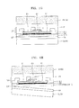
- the method may further include forming an insulating layer covering the device portion and disposed between the device portion and the second substrate; and etching portions of the insulating layer and the gate insulating layer to expose the source electrode, the drain electrode, and the gate.
- the source electrode and the drain electrode may be formed to respectively include a first pad portion and a second pad portion, and the method may further include etching portions of the gate insulating layer to expose the first and second pad portions.
- a portion of the gate insulating layer extended onto the first insulating layer may have the same height as the graphene layer.
- Example embodiments are described herein with reference to cross-sectional illustrations that are schematic illustrations of idealized embodiments (and intermediate structures) of example embodiments. As such, variations from the shapes of the illustrations as a result, for example, of manufacturing techniques and/or tolerances, are to be expected. Thus, example embodiments should not be construed as limited to the particular shapes of regions illustrated herein but are to include deviations in shapes that result, for example, from manufacturing. For example, an implanted region illustrated as a rectangle will, typically, have rounded or curved features and/or a gradient of implant concentration at its edges rather than a binary change from implanted to non-implanted region.
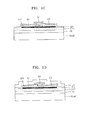
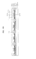
- the conductive layer SD1 may be etched.
- a source electrode S1 and a drain electrode D1 may be formed.
- the structure as illustrated in FIG. 1B may be obtained.
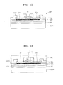
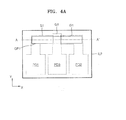
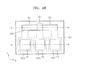
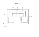
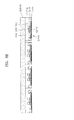
- the graphene device portion may include a gate G1, a gate insulating layer GI1 formed on the gate G1, a source electrode S1 and a drain electrode D1 formed on the gate insulating layer GI1 at two sides of the gate G1, and a graphene layer GP1 formed to contact the source electrode S1 and the drain electrode D1.
- the graphene layer GP1 may be a channel layer.
- the gate insulating layer GI1 may extend onto the first insulating layer IL1 around the graphene layer GP1.
- a portion of the gate insulating layer GI1 extended onto the first insulating layer IL1 may be disposed at the same (or similar) height as the graphene layer GP1.
- the gate G1 may overlap with the source electrode S1 and the drain electrode D1.
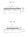
- a second insulating layer IL2 covering the graphene layer GP1 and the gate insulating layer GI1 may be further provided.
Landscapes
- Thin Film Transistor (AREA)
- Carbon And Carbon Compounds (AREA)
Applications Claiming Priority (1)
| Application Number | Priority Date | Filing Date | Title |
|---|---|---|---|
| KR1020120007797A KR101946005B1 (ko) | 2012-01-26 | 2012-01-26 | 그래핀 소자 및 그 제조방법 |
Publications (3)
| Publication Number | Publication Date |
|---|---|
| EP2620982A2 true EP2620982A2 (fr) | 2013-07-31 |
| EP2620982A3 EP2620982A3 (fr) | 2015-05-13 |
| EP2620982B1 EP2620982B1 (fr) | 2019-04-03 |
Family
ID=47080228
Family Applications (1)
| Application Number | Title | Priority Date | Filing Date |
|---|---|---|---|
| EP13150824.4A Active EP2620982B1 (fr) | 2012-01-26 | 2013-01-10 | Dispositif de graphène et son procédé de fabrication |
Country Status (4)
| Country | Link |
|---|---|
| US (1) | US9006044B2 (fr) |
| EP (1) | EP2620982B1 (fr) |
| KR (1) | KR101946005B1 (fr) |
| CN (1) | CN103227103B (fr) |
Cited By (3)
| Publication number | Priority date | Publication date | Assignee | Title |
|---|---|---|---|---|
| EP3131121A1 (fr) * | 2015-08-12 | 2017-02-15 | Nokia Technologies Oy | Appareil à effet de champ à base de graphène et procédés associés |
| EP3136445A1 (fr) * | 2015-08-25 | 2017-03-01 | Emberion Oy | Procédé de formation d'un appareil comprenant un matériau bidimensionnel |
| EP3136443A1 (fr) * | 2015-08-28 | 2017-03-01 | Nokia Technologies Oy | Procédé de formation d'un appareil comprenant un matériau bidimensionnel |
Families Citing this family (26)
| Publication number | Priority date | Publication date | Assignee | Title |
|---|---|---|---|---|
| US9721825B2 (en) | 2008-12-02 | 2017-08-01 | Arizona Board Of Regents, A Body Corporate Of The State Of Arizona, Acting For And On Behalf Of Arizona State University | Method of providing a flexible semiconductor device and flexible semiconductor device thereof |
| US9601530B2 (en) | 2008-12-02 | 2017-03-21 | Arizona Board Of Regents, A Body Corporated Of The State Of Arizona, Acting For And On Behalf Of Arizona State University | Dual active layer semiconductor device and method of manufacturing the same |
| US9991311B2 (en) | 2008-12-02 | 2018-06-05 | Arizona Board Of Regents On Behalf Of Arizona State University | Dual active layer semiconductor device and method of manufacturing the same |
| FR2998092B1 (fr) * | 2012-11-13 | 2014-11-07 | Commissariat Energie Atomique | Interposeur en graphene et procede de fabrication d'un tel interposeur |
| CN103839821B (zh) * | 2012-11-27 | 2016-08-31 | 中芯国际集成电路制造(上海)有限公司 | 晶体管及其制造方法 |
| US10381224B2 (en) | 2014-01-23 | 2019-08-13 | Arizona Board Of Regents On Behalf Of Arizona State University | Method of providing an electronic device and electronic device thereof |
| WO2017034644A2 (fr) | 2015-06-09 | 2017-03-02 | ARIZONA BOARD OF REGENTS a body corporate for THE STATE OF ARIZONA for and on behalf of ARIZONA STATE UNIVERSITY | Procédé permettant d'obtenir un dispositif électronique et dispositif électronique correspondant |
| WO2015156891A2 (fr) | 2014-01-23 | 2015-10-15 | Arizona Board Of Regents, Acting For And On Behalf Of Arizona State University | Procédé de fabrication d'un dispositif à semi-conducteur souple et dispositif à semi-conducteur souple associé |
| KR102153931B1 (ko) * | 2014-01-28 | 2020-09-10 | 한국전자통신연구원 | 그래핀 나노 소자의 제조 방법 |
| KR102466741B1 (ko) | 2014-05-13 | 2022-11-15 | 아리조나 보드 오브 리젠츠 온 비하프 오브 아리조나 스테이트 유니버시티 | 전자 디바이스를 제공하는 방법 |
| KR101714836B1 (ko) * | 2014-09-12 | 2017-03-10 | 한양대학교 산학협력단 | 전자 소자, 및 그 제조 방법 |
| KR101714837B1 (ko) * | 2014-09-12 | 2017-03-10 | 한양대학교 산학협력단 | 전자 소자, 및 그 제조 방법 |
| US10446582B2 (en) | 2014-12-22 | 2019-10-15 | Arizona Board Of Regents On Behalf Of Arizona State University | Method of providing an imaging system and imaging system thereof |
| US9741742B2 (en) | 2014-12-22 | 2017-08-22 | Arizona Board Of Regents, A Body Corporate Of The State Of Arizona, Acting For And On Behalf Of Arizona State University | Deformable electronic device and methods of providing and using deformable electronic device |
| KR102335773B1 (ko) | 2015-04-30 | 2021-12-06 | 삼성전자주식회사 | 그래핀을 포함한 2d 물질을 사용한 유연소자 및 그 제조방법 |
| CN105140284A (zh) * | 2015-07-28 | 2015-12-09 | 国家纳米科学中心 | 一种石墨烯场效应晶体管及其制作方法 |
| CN105609539B (zh) * | 2015-12-22 | 2019-01-04 | 电子科技大学 | 自对准二维晶体材料场效应半导体器件及其制备方法 |
| US10665799B2 (en) * | 2016-07-14 | 2020-05-26 | International Business Machines Corporation | N-type end-bonded metal contacts for carbon nanotube transistors |
| CN107840325B (zh) * | 2016-09-19 | 2019-09-17 | 上海和辉光电有限公司 | 一种石墨烯的制备方法 |
| CN106744660A (zh) * | 2016-12-26 | 2017-05-31 | 电子科技大学 | 一种可拉伸柔性电子器件的制作方法 |
| KR102521397B1 (ko) * | 2017-03-07 | 2023-04-14 | 주성엔지니어링(주) | 기판 처리장치 및 이를 이용한 기판 처리방법 |
| US20180308696A1 (en) * | 2017-04-25 | 2018-10-25 | Texas Instruments Incorporated | Low contact resistance graphene device integration |
| CN110100303B (zh) * | 2017-11-28 | 2021-04-20 | 华为技术有限公司 | 一种石墨烯晶体管的制备方法 |
| CN110137075B (zh) * | 2019-05-14 | 2021-06-11 | 南京中电芯谷高频器件产业技术研究院有限公司 | 一种离子注入氧化实现自对准石墨烯晶体管的制造方法 |
| CN111653478B (zh) * | 2020-03-13 | 2022-06-28 | 厦门市三安集成电路有限公司 | 一种制作增强型氮化镓功率器件的方法 |
| EP4391022B1 (fr) * | 2022-12-23 | 2026-01-07 | Graphenea Semiconductor S.L.U. | Dispositif à base de graphène et procédé de métallisation d'un dispositif à base de graphène |
Family Cites Families (14)
| Publication number | Priority date | Publication date | Assignee | Title |
|---|---|---|---|---|
| JP5135825B2 (ja) | 2007-02-21 | 2013-02-06 | 富士通株式会社 | グラフェントランジスタ及びその製造方法 |
| US7858989B2 (en) | 2008-08-29 | 2010-12-28 | Globalfoundries Inc. | Device and process of forming device with device structure formed in trench and graphene layer formed thereover |
| US7856040B2 (en) * | 2008-09-24 | 2010-12-21 | Palo Alto Research Center Incorporated | Semiconductor light emitting devices with non-epitaxial upper cladding |
| JP5409084B2 (ja) * | 2009-04-06 | 2014-02-05 | キヤノン株式会社 | 半導体装置の製造方法 |
| US8895352B2 (en) | 2009-06-02 | 2014-11-25 | International Business Machines Corporation | Method to improve nucleation of materials on graphene and carbon nanotubes |
| US8409366B2 (en) | 2009-06-23 | 2013-04-02 | Oki Data Corporation | Separation method of nitride semiconductor layer, semiconductor device, manufacturing method thereof, semiconductor wafer, and manufacturing method thereof |
| JP5544796B2 (ja) * | 2009-09-10 | 2014-07-09 | ソニー株式会社 | 3端子型電子デバイス及び2端子型電子デバイス |
| KR101736462B1 (ko) * | 2009-09-21 | 2017-05-16 | 한화테크윈 주식회사 | 그래핀의 제조 방법 |
| US8673703B2 (en) | 2009-11-17 | 2014-03-18 | International Business Machines Corporation | Fabrication of graphene nanoelectronic devices on SOI structures |
| CN101834206B (zh) * | 2010-04-12 | 2012-10-10 | 清华大学 | 半导体器件结构及其形成方法 |
| US9024300B2 (en) * | 2010-05-13 | 2015-05-05 | Nokia Corporation | Manufacture of graphene-based apparatus |
| US8445320B2 (en) * | 2010-05-20 | 2013-05-21 | International Business Machines Corporation | Graphene channel-based devices and methods for fabrication thereof |
| US8748871B2 (en) * | 2011-01-19 | 2014-06-10 | International Business Machines Corporation | Graphene devices and semiconductor field effect transistors in 3D hybrid integrated circuits |
| KR101878739B1 (ko) | 2011-10-24 | 2018-07-17 | 삼성전자주식회사 | 그래핀 전사부재, 그래핀 전사방법 및 이를 이용한 그래핀 소자 제조방법 |
-
2012
- 2012-01-26 KR KR1020120007797A patent/KR101946005B1/ko active Active
- 2012-07-11 US US13/546,615 patent/US9006044B2/en active Active
- 2012-11-29 CN CN201210497438.6A patent/CN103227103B/zh active Active
-
2013
- 2013-01-10 EP EP13150824.4A patent/EP2620982B1/fr active Active
Non-Patent Citations (1)
| Title |
|---|
| None |
Cited By (7)
| Publication number | Priority date | Publication date | Assignee | Title |
|---|---|---|---|---|
| EP3131121A1 (fr) * | 2015-08-12 | 2017-02-15 | Nokia Technologies Oy | Appareil à effet de champ à base de graphène et procédés associés |
| WO2017025661A1 (fr) * | 2015-08-12 | 2017-02-16 | Nokia Technologies Oy | Appareil à effet de champ et procédés associés |
| EP3136445A1 (fr) * | 2015-08-25 | 2017-03-01 | Emberion Oy | Procédé de formation d'un appareil comprenant un matériau bidimensionnel |
| US10396180B2 (en) | 2015-08-25 | 2019-08-27 | Emberion Oy | Method for forming apparatus comprising two dimensional material |
| EP3136443A1 (fr) * | 2015-08-28 | 2017-03-01 | Nokia Technologies Oy | Procédé de formation d'un appareil comprenant un matériau bidimensionnel |
| WO2017037333A1 (fr) * | 2015-08-28 | 2017-03-09 | Nokia Technologies Oy | Procédé de formation d'appareil comprenant un matériau bidimensionnel |
| US10868121B2 (en) | 2015-08-28 | 2020-12-15 | Nokia Technologies Oy | Method for forming apparatus comprising two dimensional material |
Also Published As
| Publication number | Publication date |
|---|---|
| CN103227103A (zh) | 2013-07-31 |
| US20130193411A1 (en) | 2013-08-01 |
| KR101946005B1 (ko) | 2019-02-08 |
| KR20130086807A (ko) | 2013-08-05 |
| EP2620982B1 (fr) | 2019-04-03 |
| EP2620982A3 (fr) | 2015-05-13 |
| CN103227103B (zh) | 2017-06-23 |
| US9006044B2 (en) | 2015-04-14 |
Similar Documents
| Publication | Publication Date | Title |
|---|---|---|
| EP2620982B1 (fr) | Dispositif de graphène et son procédé de fabrication | |
| US9293596B2 (en) | Graphene devices and methods of manufacturing the same | |
| US9257508B2 (en) | Transistors and methods of manufacturing the same | |
| US9214559B2 (en) | Graphene-transferring member, graphene transferrer, method of transferring graphene, and methods of fabricating graphene device by using the same | |
| US9040958B2 (en) | Transistors and methods of manufacturing the same | |
| US9196478B2 (en) | Graphene transferring methods, device manufacturing method using the same, and substrate structures including graphene | |
| US8344358B2 (en) | Graphene transistor with a self-aligned gate | |
| US20140104793A1 (en) | Stretchable electronic device and method of manufacturing same | |
| CN102738237B (zh) | 石墨烯电子器件及其制造方法 | |
| TW586165B (en) | Self-aligned nanotube field effect transistor and method of fabricating same | |
| US7972930B2 (en) | Transistor and method of manufacturing the same | |
| US8274072B2 (en) | Ultrathin spacer formation for carbon-based FET | |
| KR101564038B1 (ko) | 패턴화된 그래핀의 직접 성장 방법 | |
| KR20140044763A (ko) | 높은 변형률에도 안정적인 거동을 가지는 절연체 및 게이트 전극을 포함하는 그래핀 전계효과 트랜지스터, 및 이의 제조 방법 | |
| US20170170012A1 (en) | Method of intercalating insulating layer between metal catalyst layer and graphene layer and method of fabricating semiconductor device using the same |
Legal Events
| Date | Code | Title | Description |
|---|---|---|---|
| PUAI | Public reference made under article 153(3) epc to a published international application that has entered the european phase |
Free format text: ORIGINAL CODE: 0009012 |
|
| AK | Designated contracting states |
Kind code of ref document: A2 Designated state(s): AL AT BE BG CH CY CZ DE DK EE ES FI FR GB GR HR HU IE IS IT LI LT LU LV MC MK MT NL NO PL PT RO RS SE SI SK SM TR |
|
| AX | Request for extension of the european patent |
Extension state: BA ME |
|
| PUAL | Search report despatched |
Free format text: ORIGINAL CODE: 0009013 |
|
| AK | Designated contracting states |
Kind code of ref document: A3 Designated state(s): AL AT BE BG CH CY CZ DE DK EE ES FI FR GB GR HR HU IE IS IT LI LT LU LV MC MK MT NL NO PL PT RO RS SE SI SK SM TR |
|
| AX | Request for extension of the european patent |
Extension state: BA ME |
|
| RIC1 | Information provided on ipc code assigned before grant |
Ipc: H01L 21/683 20060101ALN20150408BHEP Ipc: H01L 29/778 20060101AFI20150408BHEP Ipc: H01L 29/417 20060101ALN20150408BHEP Ipc: H01L 29/16 20060101ALI20150408BHEP |
|
| 17P | Request for examination filed |
Effective date: 20151113 |
|
| RBV | Designated contracting states (corrected) |
Designated state(s): AL AT BE BG CH CY CZ DE DK EE ES FI FR GB GR HR HU IE IS IT LI LT LU LV MC MK MT NL NO PL PT RO RS SE SI SK SM TR |
|
| 17Q | First examination report despatched |
Effective date: 20160428 |
|
| GRAP | Despatch of communication of intention to grant a patent |
Free format text: ORIGINAL CODE: EPIDOSNIGR1 |
|
| STAA | Information on the status of an ep patent application or granted ep patent |
Free format text: STATUS: GRANT OF PATENT IS INTENDED |
|
| RIC1 | Information provided on ipc code assigned before grant |
Ipc: H01L 29/778 20060101AFI20181203BHEP Ipc: H01L 29/417 20060101ALN20181203BHEP Ipc: H01L 29/16 20060101ALI20181203BHEP Ipc: H01L 21/683 20060101ALN20181203BHEP |
|
| INTG | Intention to grant announced |
Effective date: 20190109 |
|
| GRAS | Grant fee paid |
Free format text: ORIGINAL CODE: EPIDOSNIGR3 |
|
| GRAA | (expected) grant |
Free format text: ORIGINAL CODE: 0009210 |
|
| STAA | Information on the status of an ep patent application or granted ep patent |
Free format text: STATUS: THE PATENT HAS BEEN GRANTED |
|
| AK | Designated contracting states |
Kind code of ref document: B1 Designated state(s): AL AT BE BG CH CY CZ DE DK EE ES FI FR GB GR HR HU IE IS IT LI LT LU LV MC MK MT NL NO PL PT RO RS SE SI SK SM TR |
|
| REG | Reference to a national code |
Ref country code: GB Ref legal event code: FG4D |
|
| REG | Reference to a national code |
Ref country code: CH Ref legal event code: EP Ref country code: AT Ref legal event code: REF Ref document number: 1116787 Country of ref document: AT Kind code of ref document: T Effective date: 20190415 |
|
| REG | Reference to a national code |
Ref country code: DE Ref legal event code: R096 Ref document number: 602013053175 Country of ref document: DE |
|
| REG | Reference to a national code |
Ref country code: IE Ref legal event code: FG4D |
|
| REG | Reference to a national code |
Ref country code: NL Ref legal event code: MP Effective date: 20190403 |
|
| REG | Reference to a national code |
Ref country code: LT Ref legal event code: MG4D |
|
| REG | Reference to a national code |
Ref country code: AT Ref legal event code: MK05 Ref document number: 1116787 Country of ref document: AT Kind code of ref document: T Effective date: 20190403 |
|
| PG25 | Lapsed in a contracting state [announced via postgrant information from national office to epo] |
Ref country code: NL Free format text: LAPSE BECAUSE OF FAILURE TO SUBMIT A TRANSLATION OF THE DESCRIPTION OR TO PAY THE FEE WITHIN THE PRESCRIBED TIME-LIMIT Effective date: 20190403 |
|
| PG25 | Lapsed in a contracting state [announced via postgrant information from national office to epo] |
Ref country code: ES Free format text: LAPSE BECAUSE OF FAILURE TO SUBMIT A TRANSLATION OF THE DESCRIPTION OR TO PAY THE FEE WITHIN THE PRESCRIBED TIME-LIMIT Effective date: 20190403 Ref country code: SE Free format text: LAPSE BECAUSE OF FAILURE TO SUBMIT A TRANSLATION OF THE DESCRIPTION OR TO PAY THE FEE WITHIN THE PRESCRIBED TIME-LIMIT Effective date: 20190403 Ref country code: FI Free format text: LAPSE BECAUSE OF FAILURE TO SUBMIT A TRANSLATION OF THE DESCRIPTION OR TO PAY THE FEE WITHIN THE PRESCRIBED TIME-LIMIT Effective date: 20190403 Ref country code: PT Free format text: LAPSE BECAUSE OF FAILURE TO SUBMIT A TRANSLATION OF THE DESCRIPTION OR TO PAY THE FEE WITHIN THE PRESCRIBED TIME-LIMIT Effective date: 20190803 Ref country code: NO Free format text: LAPSE BECAUSE OF FAILURE TO SUBMIT A TRANSLATION OF THE DESCRIPTION OR TO PAY THE FEE WITHIN THE PRESCRIBED TIME-LIMIT Effective date: 20190703 Ref country code: AL Free format text: LAPSE BECAUSE OF FAILURE TO SUBMIT A TRANSLATION OF THE DESCRIPTION OR TO PAY THE FEE WITHIN THE PRESCRIBED TIME-LIMIT Effective date: 20190403 Ref country code: LT Free format text: LAPSE BECAUSE OF FAILURE TO SUBMIT A TRANSLATION OF THE DESCRIPTION OR TO PAY THE FEE WITHIN THE PRESCRIBED TIME-LIMIT Effective date: 20190403 Ref country code: HR Free format text: LAPSE BECAUSE OF FAILURE TO SUBMIT A TRANSLATION OF THE DESCRIPTION OR TO PAY THE FEE WITHIN THE PRESCRIBED TIME-LIMIT Effective date: 20190403 Ref country code: CZ Free format text: LAPSE BECAUSE OF FAILURE TO SUBMIT A TRANSLATION OF THE DESCRIPTION OR TO PAY THE FEE WITHIN THE PRESCRIBED TIME-LIMIT Effective date: 20190403 |
|
| PG25 | Lapsed in a contracting state [announced via postgrant information from national office to epo] |
Ref country code: LV Free format text: LAPSE BECAUSE OF FAILURE TO SUBMIT A TRANSLATION OF THE DESCRIPTION OR TO PAY THE FEE WITHIN THE PRESCRIBED TIME-LIMIT Effective date: 20190403 Ref country code: RS Free format text: LAPSE BECAUSE OF FAILURE TO SUBMIT A TRANSLATION OF THE DESCRIPTION OR TO PAY THE FEE WITHIN THE PRESCRIBED TIME-LIMIT Effective date: 20190403 Ref country code: BG Free format text: LAPSE BECAUSE OF FAILURE TO SUBMIT A TRANSLATION OF THE DESCRIPTION OR TO PAY THE FEE WITHIN THE PRESCRIBED TIME-LIMIT Effective date: 20190703 Ref country code: GR Free format text: LAPSE BECAUSE OF FAILURE TO SUBMIT A TRANSLATION OF THE DESCRIPTION OR TO PAY THE FEE WITHIN THE PRESCRIBED TIME-LIMIT Effective date: 20190704 Ref country code: PL Free format text: LAPSE BECAUSE OF FAILURE TO SUBMIT A TRANSLATION OF THE DESCRIPTION OR TO PAY THE FEE WITHIN THE PRESCRIBED TIME-LIMIT Effective date: 20190403 |
|
| PG25 | Lapsed in a contracting state [announced via postgrant information from national office to epo] |
Ref country code: IS Free format text: LAPSE BECAUSE OF FAILURE TO SUBMIT A TRANSLATION OF THE DESCRIPTION OR TO PAY THE FEE WITHIN THE PRESCRIBED TIME-LIMIT Effective date: 20190803 Ref country code: AT Free format text: LAPSE BECAUSE OF FAILURE TO SUBMIT A TRANSLATION OF THE DESCRIPTION OR TO PAY THE FEE WITHIN THE PRESCRIBED TIME-LIMIT Effective date: 20190403 |
|
| REG | Reference to a national code |
Ref country code: DE Ref legal event code: R097 Ref document number: 602013053175 Country of ref document: DE |
|
| PG25 | Lapsed in a contracting state [announced via postgrant information from national office to epo] |
Ref country code: DK Free format text: LAPSE BECAUSE OF FAILURE TO SUBMIT A TRANSLATION OF THE DESCRIPTION OR TO PAY THE FEE WITHIN THE PRESCRIBED TIME-LIMIT Effective date: 20190403 Ref country code: EE Free format text: LAPSE BECAUSE OF FAILURE TO SUBMIT A TRANSLATION OF THE DESCRIPTION OR TO PAY THE FEE WITHIN THE PRESCRIBED TIME-LIMIT Effective date: 20190403 Ref country code: SK Free format text: LAPSE BECAUSE OF FAILURE TO SUBMIT A TRANSLATION OF THE DESCRIPTION OR TO PAY THE FEE WITHIN THE PRESCRIBED TIME-LIMIT Effective date: 20190403 Ref country code: RO Free format text: LAPSE BECAUSE OF FAILURE TO SUBMIT A TRANSLATION OF THE DESCRIPTION OR TO PAY THE FEE WITHIN THE PRESCRIBED TIME-LIMIT Effective date: 20190403 |
|
| PLBE | No opposition filed within time limit |
Free format text: ORIGINAL CODE: 0009261 |
|
| STAA | Information on the status of an ep patent application or granted ep patent |
Free format text: STATUS: NO OPPOSITION FILED WITHIN TIME LIMIT |
|
| PG25 | Lapsed in a contracting state [announced via postgrant information from national office to epo] |
Ref country code: SM Free format text: LAPSE BECAUSE OF FAILURE TO SUBMIT A TRANSLATION OF THE DESCRIPTION OR TO PAY THE FEE WITHIN THE PRESCRIBED TIME-LIMIT Effective date: 20190403 Ref country code: IT Free format text: LAPSE BECAUSE OF FAILURE TO SUBMIT A TRANSLATION OF THE DESCRIPTION OR TO PAY THE FEE WITHIN THE PRESCRIBED TIME-LIMIT Effective date: 20190403 |
|
| 26N | No opposition filed |
Effective date: 20200106 |
|
| PG25 | Lapsed in a contracting state [announced via postgrant information from national office to epo] |
Ref country code: TR Free format text: LAPSE BECAUSE OF FAILURE TO SUBMIT A TRANSLATION OF THE DESCRIPTION OR TO PAY THE FEE WITHIN THE PRESCRIBED TIME-LIMIT Effective date: 20190403 |
|
| PG25 | Lapsed in a contracting state [announced via postgrant information from national office to epo] |
Ref country code: SI Free format text: LAPSE BECAUSE OF FAILURE TO SUBMIT A TRANSLATION OF THE DESCRIPTION OR TO PAY THE FEE WITHIN THE PRESCRIBED TIME-LIMIT Effective date: 20190403 |
|
| PG25 | Lapsed in a contracting state [announced via postgrant information from national office to epo] |
Ref country code: MC Free format text: LAPSE BECAUSE OF FAILURE TO SUBMIT A TRANSLATION OF THE DESCRIPTION OR TO PAY THE FEE WITHIN THE PRESCRIBED TIME-LIMIT Effective date: 20190403 |
|
| REG | Reference to a national code |
Ref country code: CH Ref legal event code: PL |
|
| REG | Reference to a national code |
Ref country code: BE Ref legal event code: MM Effective date: 20200131 |
|
| PG25 | Lapsed in a contracting state [announced via postgrant information from national office to epo] |
Ref country code: LU Free format text: LAPSE BECAUSE OF NON-PAYMENT OF DUE FEES Effective date: 20200110 |
|
| PG25 | Lapsed in a contracting state [announced via postgrant information from national office to epo] |
Ref country code: LI Free format text: LAPSE BECAUSE OF NON-PAYMENT OF DUE FEES Effective date: 20200131 Ref country code: CH Free format text: LAPSE BECAUSE OF NON-PAYMENT OF DUE FEES Effective date: 20200131 Ref country code: BE Free format text: LAPSE BECAUSE OF NON-PAYMENT OF DUE FEES Effective date: 20200131 |
|
| PG25 | Lapsed in a contracting state [announced via postgrant information from national office to epo] |
Ref country code: IE Free format text: LAPSE BECAUSE OF NON-PAYMENT OF DUE FEES Effective date: 20200110 |
|
| PG25 | Lapsed in a contracting state [announced via postgrant information from national office to epo] |
Ref country code: MT Free format text: LAPSE BECAUSE OF FAILURE TO SUBMIT A TRANSLATION OF THE DESCRIPTION OR TO PAY THE FEE WITHIN THE PRESCRIBED TIME-LIMIT Effective date: 20190403 Ref country code: CY Free format text: LAPSE BECAUSE OF FAILURE TO SUBMIT A TRANSLATION OF THE DESCRIPTION OR TO PAY THE FEE WITHIN THE PRESCRIBED TIME-LIMIT Effective date: 20190403 |
|
| PG25 | Lapsed in a contracting state [announced via postgrant information from national office to epo] |
Ref country code: MK Free format text: LAPSE BECAUSE OF FAILURE TO SUBMIT A TRANSLATION OF THE DESCRIPTION OR TO PAY THE FEE WITHIN THE PRESCRIBED TIME-LIMIT Effective date: 20190403 |
|
| P01 | Opt-out of the competence of the unified patent court (upc) registered |
Effective date: 20230519 |
|
| REG | Reference to a national code |
Ref country code: DE Ref legal event code: R079 Ref document number: 602013053175 Country of ref document: DE Free format text: PREVIOUS MAIN CLASS: H01L0029778000 Ipc: H10D0030470000 |
|
| PGFP | Annual fee paid to national office [announced via postgrant information from national office to epo] |
Ref country code: GB Payment date: 20251211 Year of fee payment: 14 |
|
| PGFP | Annual fee paid to national office [announced via postgrant information from national office to epo] |
Ref country code: FR Payment date: 20251222 Year of fee payment: 14 |
|
| PGFP | Annual fee paid to national office [announced via postgrant information from national office to epo] |
Ref country code: DE Payment date: 20251216 Year of fee payment: 14 |