EP2621031A2 - Agencement optique et procédé destinés à générer des impulsions lumineuses à décélération variable - Google Patents
Agencement optique et procédé destinés à générer des impulsions lumineuses à décélération variable Download PDFInfo
- Publication number
- EP2621031A2 EP2621031A2 EP13000268.6A EP13000268A EP2621031A2 EP 2621031 A2 EP2621031 A2 EP 2621031A2 EP 13000268 A EP13000268 A EP 13000268A EP 2621031 A2 EP2621031 A2 EP 2621031A2
- Authority
- EP
- European Patent Office
- Prior art keywords
- pulse
- light pulses
- light source
- temperature
- delay element
- Prior art date
- Legal status (The legal status is an assumption and is not a legal conclusion. Google has not performed a legal analysis and makes no representation as to the accuracy of the status listed.)
- Granted
Links
Images





Classifications
-
- H—ELECTRICITY
- H01—ELECTRIC ELEMENTS
- H01S—DEVICES USING THE PROCESS OF LIGHT AMPLIFICATION BY STIMULATED EMISSION OF RADIATION [LASER] TO AMPLIFY OR GENERATE LIGHT; DEVICES USING STIMULATED EMISSION OF ELECTROMAGNETIC RADIATION IN WAVE RANGES OTHER THAN OPTICAL
- H01S3/00—Lasers, i.e. devices using stimulated emission of electromagnetic radiation in the infrared, visible or ultraviolet wave range
- H01S3/10—Controlling the intensity, frequency, phase, polarisation or direction of the emitted radiation, e.g. switching, gating, modulating or demodulating
-
- H—ELECTRICITY
- H01—ELECTRIC ELEMENTS
- H01S—DEVICES USING THE PROCESS OF LIGHT AMPLIFICATION BY STIMULATED EMISSION OF RADIATION [LASER] TO AMPLIFY OR GENERATE LIGHT; DEVICES USING STIMULATED EMISSION OF ELECTROMAGNETIC RADIATION IN WAVE RANGES OTHER THAN OPTICAL
- H01S5/00—Semiconductor lasers
- H01S5/005—Optical components external to the laser cavity, specially adapted therefor, e.g. for homogenisation or merging of the beams or for manipulating laser pulses, e.g. pulse shaping
- H01S5/0057—Optical components external to the laser cavity, specially adapted therefor, e.g. for homogenisation or merging of the beams or for manipulating laser pulses, e.g. pulse shaping for temporal shaping, e.g. pulse compression, frequency chirping
-
- G—PHYSICS
- G01—MEASURING; TESTING
- G01J—MEASUREMENT OF INTENSITY, VELOCITY, SPECTRAL CONTENT, POLARISATION, PHASE OR PULSE CHARACTERISTICS OF INFRARED, VISIBLE OR ULTRAVIOLET LIGHT; COLORIMETRY; RADIATION PYROMETRY
- G01J11/00—Measuring the characteristics of individual optical pulses or of optical pulse trains
-
- G—PHYSICS
- G01—MEASURING; TESTING
- G01J—MEASUREMENT OF INTENSITY, VELOCITY, SPECTRAL CONTENT, POLARISATION, PHASE OR PULSE CHARACTERISTICS OF INFRARED, VISIBLE OR ULTRAVIOLET LIGHT; COLORIMETRY; RADIATION PYROMETRY
- G01J3/00—Spectrometry; Spectrophotometry; Monochromators; Measuring colours
- G01J3/02—Details
- G01J3/0286—Constructional arrangements for compensating for fluctuations caused by temperature, humidity or pressure, or using cooling or temperature stabilization of parts of the device; Controlling the atmosphere inside a spectrometer, e.g. vacuum
-
- G—PHYSICS
- G01—MEASURING; TESTING
- G01J—MEASUREMENT OF INTENSITY, VELOCITY, SPECTRAL CONTENT, POLARISATION, PHASE OR PULSE CHARACTERISTICS OF INFRARED, VISIBLE OR ULTRAVIOLET LIGHT; COLORIMETRY; RADIATION PYROMETRY
- G01J3/00—Spectrometry; Spectrophotometry; Monochromators; Measuring colours
- G01J3/02—Details
- G01J3/10—Arrangements of light sources specially adapted for spectrometry or colorimetry
-
- G—PHYSICS
- G01—MEASURING; TESTING
- G01N—INVESTIGATING OR ANALYSING MATERIALS BY DETERMINING THEIR CHEMICAL OR PHYSICAL PROPERTIES
- G01N21/00—Investigating or analysing materials by the use of optical means, i.e. using sub-millimetre waves, infrared, visible or ultraviolet light
- G01N21/17—Systems in which incident light is modified in accordance with the properties of the material investigated
- G01N21/25—Colour; Spectral properties, i.e. comparison of effect of material on the light at two or more different wavelengths or wavelength bands
- G01N21/31—Investigating relative effect of material at wavelengths characteristic of specific elements or molecules, e.g. atomic absorption spectrometry
- G01N21/35—Investigating relative effect of material at wavelengths characteristic of specific elements or molecules, e.g. atomic absorption spectrometry using infrared light
- G01N21/3581—Investigating relative effect of material at wavelengths characteristic of specific elements or molecules, e.g. atomic absorption spectrometry using infrared light using far infrared light; using Terahertz radiation
-
- G—PHYSICS
- G01—MEASURING; TESTING
- G01N—INVESTIGATING OR ANALYSING MATERIALS BY DETERMINING THEIR CHEMICAL OR PHYSICAL PROPERTIES
- G01N21/00—Investigating or analysing materials by the use of optical means, i.e. using sub-millimetre waves, infrared, visible or ultraviolet light
- G01N21/62—Systems in which the material investigated is excited whereby it emits light or causes a change in wavelength of the incident light
- G01N21/63—Systems in which the material investigated is excited whereby it emits light or causes a change in wavelength of the incident light optically excited
- G01N21/636—Systems in which the material investigated is excited whereby it emits light or causes a change in wavelength of the incident light optically excited using an arrangement of pump beam and probe beam; using the measurement of optical non-linear properties
-
- G—PHYSICS
- G01—MEASURING; TESTING
- G01N—INVESTIGATING OR ANALYSING MATERIALS BY DETERMINING THEIR CHEMICAL OR PHYSICAL PROPERTIES
- G01N21/00—Investigating or analysing materials by the use of optical means, i.e. using sub-millimetre waves, infrared, visible or ultraviolet light
- G01N21/17—Systems in which incident light is modified in accordance with the properties of the material investigated
- G01N21/25—Colour; Spectral properties, i.e. comparison of effect of material on the light at two or more different wavelengths or wavelength bands
- G01N21/31—Investigating relative effect of material at wavelengths characteristic of specific elements or molecules, e.g. atomic absorption spectrometry
- G01N21/35—Investigating relative effect of material at wavelengths characteristic of specific elements or molecules, e.g. atomic absorption spectrometry using infrared light
- G01N2021/3595—Investigating relative effect of material at wavelengths characteristic of specific elements or molecules, e.g. atomic absorption spectrometry using infrared light using FTIR
Definitions
- the invention relates to an optical arrangement according to the preamble of claim 1, and to a corresponding method.
- a generic optical arrangement or a corresponding method is known under the name "optical sampling by cavity tuning (OSCAT)", for example from the DE 10 2008 026 484 A1 , from the article "Optical sampling by laser cavity tuning ", T. Hochrein, R. Wilk, M. Mei, R. Holzwarth, N. Krumbholz, M. Koch, OPTICS Express 1613, Vol. 18, No. 2, January 2010 , or from the article " OSCAT: Novel Technique for Time-Resolved Experiments Without Movable Optical Delay Lines ", R. Wilk, T. Hochrein, M. Koch, M. Mei, R. Holzwarth, J Infrared Milli Terahz Waves (2011) 32: 596-602 ,
- the principle behind the OSCAT method is based on the fact that a pulsed light source emits a series of light pulses. These light pulses are split at a pulse or beam splitter into sequences of first and second secondary light pulses, respectively.
- a delay line or generally a delay element In the traversed by the second secondary light pulses path is a delay line or generally a delay element, which provides for a time delay of the second secondary laser pulses relative to the first secondary laser pulses.
- the OSCAT method now makes it possible to variably set a time delay of a certain second secondary light pulse relative to a first secondary light pulse, even if the time delay of the second secondary light pulse generated by the delay element remains constant or if the optical path length of the delay element remains constant. This is achieved by changing the repetition rate or (synonymously) the pulse repetition rate of the pulsed light source. For this purpose, for example, a resonator length of the pulse light source can be varied.
- the adjustable delay of the two light pulses relative to each other allows a number of unique applications, for example with regard to spectroscopic investigations or so-called pump-probe experiments, THz time domain spectroscopy or Fourier transform spectroscopy.
- the OSCAT method offers enormous advantages in terms of robustness, as well as lower adjustment effort and lower costs. For example, in the past has been an optical delay line changed mechanically, usually by moving one or more mirrors to change the delay caused. However, this required a high adjustment effort and a disproportionate effort for the mechanical precision of the shift.
- the object of the present invention is to improve the conventional optical arrangement or the conventional method with regard to their possible uses.
- the optical arrangement according to the invention comprises a pulsed light source for generating primary light pulses.
- This pulse light source is preferably, but not necessarily, a coherent pulsed light source, i. around a pulsed laser.
- it could be an amplitude-modulated CW semiconductor laser, but usually fashion-coupled lasers such as short-pulse or ultrashort pulse lasers, for example femtosecond lasers.
- a continuous light source e.g., a cw laser
- This pulsed light source generates a train of primary pulse with variable pulse repetition rate.
- the pulse repetition rate or repetition rate is the frequency with which the pulsed light source emits the primary light pulses.
- the pulse repetition rate is the inverse of the round trip time of a light pulse in a resonator of the pulsed light source.
- the term oscillator can also be used synonymously with the term pulse light source.
- a pulse divider is provided to divide the primary light pulses into first and second secondary light pulses.
- the term pulse divider also includes beam splitters which divide a first portion of each primary light pulse into a first light path and the remaining portion direct the primary light pulse into a second light path.
- the term Pulseiler also includes optical elements in which the two light paths coincide, so that the two secondary light pulses are indeed delivered in a common path, but staggered in succession from the pulse divider. Only the second secondary light pulses are then subject to a time delay, which is caused by a delay element.
- the optical path length of the delay element is that path length by which the length of the light path of the second secondary laser pulses differs from that of the first secondary laser pulses. This path length difference is usually fixed.
- the first and second secondary light pulses can then be directed into a target area, optionally focused in this target area.
- the target areas, in which the two secondary laser pulses are directed coincide or fall apart.
- a fiber coupler can be used as a pulse divider.
- the pulse divider may already be integrated in the pulsed light source, so that it has two output ports, which emit respectively the first and the second secondary light pulses.
- the optical arrangement according to the invention now provides a temperature insulation for thermally insulating the delay element, a temperature stabilizer for thermally stabilizing the delay element, a temperature compensator for compensating for a temperature-dependent change in an optical path length of the delay element and / or a control circuit for determining and controlling a drift of an average pulse repetition rate of the pulsed light source ,
- These four measures are both individually, as well as in any combination suitable to significantly increase the achieved with the optical arrangement precision of the time delay of two light pulses relative to each other. This precision, in turn, is critical to the accuracy and validity of the applications or experiments performed with the delayed light pulses.
- the temperature insulation of the delay element can be done for example by enclosing the delay element in temperature-insulating material such as Styrofoam or Styrodur.
- the temperature insulation causes a decoupling of the temperature of the delay element from the ambient or room temperature. This prevents that a changing room temperature on the delay element and in particular on the optical path length of the delay element and thus on the caused by the delay element delay of the light pulses influence.
- the delay element can be designed as a glass fiber.
- a temperature stabilizer also acts to decouple the temperature of the delay element from the ambient or room temperature by providing a way to keep the temperature of the delay element stable even with a change in ambient temperature.
- a setpoint temperature and a tolerance range around the setpoint temperature could be provided to initiate a return of the temperature of the delay element to the setpoint temperature when the actual temperature has moved out of the tolerance range.
- a temperature compensator in turn can accept a change in the temperature of the delay element.
- it offers the advantage of being able to compensate for a change in the optical path length of the delay element caused by the temperature increase. For example, an increase in temperature could lead to an expansion of the delay element and thus to an extension of the optical path length.
- the temperature compensator would be configured to compensate for this optical path length elongation by an element that, in turn, achieves path length shortening (and vice versa).
- the three variants mentioned above all relate to the delay element.
- the delay element so that other components of the optical assembly would be thermally insulated from the ambient temperature, so that a change in the ambient temperature can no longer have any influence on the optical arrangement and in particular on the precision of the delay of the light pulses.
- a temperature stabilizer it preferably has a temperature sensor and at least one heating element and / or at least one cooling element.
- the temperature sensor enables automation of the temperature stabilization, for example by detecting the temperature of the delay element.
- the measured value of the temperature sensor can then be suitably evaluated in order to control a heating element and / or a cooling element such that the temperature of the delay element remains within a desired range.
- the delay element could also be a specific path of an optical waveguide or an optical fiber.
- a controllable fiber stretcher as a temperature compensator. This can act on the fiber of the delay element by means of a suitable actuator, for example a piezoelectric actuator. If the temperature of the retarder changes and the fiber expands or shortens, the fiber stretcher could cause shortening or extension of the fiber of opposite sign so that the optical path length of the retarder remains constant regardless of temperature.
- a control circuit for determining and controlling a drift of an average pulse repetition rate of the pulsed light source, a frequency detector, a frequency counter or a phase detector is preferably used to determine the pulse repetition rate of the pulsed light source. In the optical arrangement according to the invention, however, the pulse repetition rate of the pulsed light source is deliberately changed in order to change the delay of the light pulses.
- the repetition rate can be stabilized to a fixed value with the aid of the phase detector (PLL, phase locked loop).
- PLL phase detector
- the signal can optionally be filtered by the frequency detector, the frequency counter or by the phase detector via a low-pass filter.
- the filtered signal can then be fed to a controller, which can influence the continuous wave source and thus its pulse repetition rate via a suitable actuator, for example an electro-optic (EOM) modulator, on the resonator length of the pulsed light source or via an amplitude modulator (AM).
- EOM electro-optic
- AM amplitude modulator
- a frequency detector which is a device that provides a voltage as a function of the current frequency.
- phase lock i.e., a coupling of the phases
- frequency lock which in principle is somewhat less accurate, since not the phase (ie directly the sine wave) is tracked. For most applications, however, this accuracy should be sufficient.
- the optics array observes the temporal position of the pulse in the experiment. If the pulse drifts, the system adjusts the pulse repetition rate.
- control loop has a function generator for specifying a constant or variable external reference frequency.
- the external reference frequency could be compared with the signal passing the low-pass filter and evaluated appropriately.
- the optical arrangement in the optical path of the first and / or the second secondary Light pulses comprises one or more of: an amplifier, an attenuator, a non-linear medium, a second harmonic generator (SHG), a pulse compressor, a pulse picker, an amplitude modulator and / or a dispersion compensator ,
- An amplifier can be realized in the form of an optically pumped and suitably doped with impurities fiber route.
- variants are conceivable in which only one amplifier is provided for the first or only for the second secondary light pulses, or wherein in each case a separate amplifier is provided for the first and the second secondary laser pulses to the peak intensity or the pulse energy of these pulses increase.
- the first and the second secondary laser pulses are brought together and directed into a common amplifier, which is thus provided for both the first and the second secondary laser pulses.
- the latter variant has the advantage of being able to amplify both the first and the second secondary laser pulses, without having to provide a second amplifier.
- an amplifier is used as a delay element, if the amplifier itself can cause an extension of an optical path length and thus a delay of light pulses. Analogously, all these possibilities also apply to an attenuator instead of an amplifier.
- a pulse compressor shortens the time duration of the first and / or second light pulses.
- a pulse picker enables the targeted picking out of one or more light pulses, e.g. to control the total irradiation of a sample.
- An amplitude modulator allows the variation of the amplitudes in a train of light pulses. This makes it possible to set not only the delay between two laser pulses at the destination, but also to delay the amplitude of the leading and / or trailing laser pulses. This allows the acquisition of both time- and intensity-dependent statements of a sample into which the first and second secondary laser pulses are directed.
- dispersion compensator which results in either the dispersion of the first secondary laser pulses corresponding exactly to that of the second secondary laser pulses as they each leave the optical array or as close as possible to the total dispersion of the first and / or second secondary laser pulses is at zero.
- a first possibility for a delay element with dispersion compensation consists of the coupling of two or more fiber types, which have opposite dispersion properties, so that the entire fiber path has effectively zero dispersion.
- a so-called IDF (inverse dispersion fiber), a DCF (dispersion compensating fiber) or a SMF (single mode fiber) could be used both in the form of a polarization-maintaining and in the form of a non-polarization-maintaining fiber.
- a second possibility is a combination of a polarization beam splitter, a circulator, non-polarization-preserving IDF, DCF, and SFM fibers, ⁇ / 4 wave plates, and a Faraday rotator.
- a third possibility is to use a fiber type that effectively has zero dispersion, such as a dispersion-shifted fiber (DSF), a photonic crystal fiber, a hollow core fiber, or a reduced non fiber -Linearticianen, again in the form of a polarization-maintaining or a non-polarization-maintaining fiber.
- DSF dispersion-shifted fiber
- a fourth possibility is the use of a fiber Bragg grating and a single-mode fiber as well as a circulator and a beam splitter. Again this version can be polarization preserving or non-polarization maintaining.
- a fifth possibility is a combination of a reflection grating or transmission grating with prisms for first or higher order dispersion compensation.
- Another possibility is the use of fiber amplifier lines with non-linear dispersion adaptation (bevel modulation) or a so-called parabolic pulse propagation.
- the invention further relates to a method for generating variable delay light pulses based on the conventional OSCAT method.
- the temperature of the delay element is kept constant by means of a temperature stabilizer, a temperature-dependent change in an optical path length of the delay element is compensated by means of a temperature compensator and / or a drift of the mean pulse repetition rate of the pulsed light source is determined and regulated, as described in detail has been described above.
- the technical advantage of these measures is a particularly high precision of the time delay between different light pulses.
- the pulse repetition rate of the pulsed light source prefferably be determined by means of a frequency detector, a frequency counter or a phase detector, and optionally a signal of the frequency counter or the phase detector to be filtered by means of a low-pass filter in order to determine the low-frequency drift of the pulse repetition rate.
- FIG. 1 shows a schematic representation of a first embodiment of an optical arrangement according to the invention 1.
- This optical arrangement 1 is designed to generate light pulses with adjustable or variable delay time between different pulses.
- the optical arrangement 1 has an oscillator or a pulse light source 2, for example a short-pulse or ultra-short pulse laser.
- the pulse light source 2 has an output port 3, at which a train of primary laser pulses 4 leaves the pulse light source 2.
- the repetition rate or the pulse repetition rate of the primary light pulses 4 is variable, for example by a resonator length of the pulse light source 2 is changed by adjusting elements such as piezo actuators.
- the optical assembly 1 further has a beam or pulse divider 5.
- This has the function to divide the primary light pulses into first and second secondary light pulses 6, 7, the pulse divider 5 on a first or on a spatially separated from the second Leave path.
- each of the primary light pulses 4 is divided into a first portion, which leaves the pulse divider 5 as the first secondary light pulse 6, and a second portion, which leaves the pulse divider 5 as a second secondary light pulse 7.
- a fiber optic or a free jet beam splitter for example a 50:50 beam splitter could be used, but also a beam splitter with a different splitting ratio.
- the optical assembly 1 further has in the path of the second secondary laser pulses via a delay element 8.
- the delay element 8 comprises in the present embodiment, a delay fiber link 9. It serves to delay the second secondary light pulses 7 relative to the first secondary light pulses 6 by the Second secondary light pulses in addition to the first light pulses in addition, the optical path length of the delay element 8 must go through. This optical path length results from the location-dependent refractive index of the delay element 8, integrated over its geometric length.
- the optical assembly 1 is capable of variably setting the time delay between the first and second secondary light pulses 6, 7 by varying the repetition rate of the pulse light source 2.
- the optical arrangement 1 has a signal generator 10.
- This signal generator 10 generates an example of a sinusoidal or sawtooth signal, with which the pulse light source 2 is fed.
- the input signal is converted in the pulse light source 2 into a corresponding change in the pulse repetition rate.
- the optical assembly 1 has a thermal insulation 12, for example, a shell of thermally insulating material.
- the insulation 12 thermally isolates its components from the environment.
- the pulse light source 2, the pulse divider 5 and the delay element 8 are within the thermal insulation 12.
- the optics assembly further has a temperature compensator 13.
- this temperature compensator 13 is designed as a controllable fiber stretcher FS. It has the task of compensating for a temperature-dependent change in an optical path length of the delay element 8 if, despite the thermal insulation 12, a slight temperature change of the delay element 8 should occur. For example, if, as the temperature increases, the optical path length of the delay fiber path 9 of the delay element 8 increases, the temperature compensator 13 could compensate for a suitable shortening of an optical fiber, and vice versa.
- a temperature sensor 14 is provided to measure the temperature of the delay element 8, in particular the delay fiber link 9. The measurement signal of the temperature sensor 14 can be used as input 15 for controlling the temperature compensator 13.
- This temperature stabilizer 16 may be used to control a temperature stabilizer 16 provided in or on the delay element 8.
- This temperature stabilizer 16 has at least one heating element 17 and / or a cooling element 18. These elements serve to keep the temperature of the delay element 8 as close as possible to a desired range defined by a desired value.
- the temperature insulation 12, the temperature stabilizer 16 and the temperature compensator 13 may also be provided individually or independently of one another in an optical arrangement 1 according to the invention.
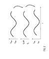
- FIG. 2 shows a schematic representation of the setting of a time delay of two secondary light pulses 6, 7.
- FIG. 2 three curves over a timeline.
- the uppermost curve shows the course of the input signal 11, with which the pulse light source 2 is fed.
- This input signal 11 varies periodically between a minimum voltage V min and a maximum voltage V max .
- the middle curve shows the change in the pulse repetition rate of the pulse light source 2 over time.
- This pulse repetition rate varies analogously to the input signal 11 between a minimum value f 0 and a maximum value f 0 + ⁇ f.
- the lowermost curve shows the time interval between two specific secondary light pulses 6, 7. This may be the time interval between two secondary pulses 6, 7, which originated from a common primary laser pulse 4, or secondary light pulses, which consist of different primary laser pulses 4 have emerged. It can be seen that the time delay also varies between a minimum value t min and a maximum value t max . Between the two upper curves and the lower curve, there are FIG. 2 However, a certain time offset, which results from the duration of the light pulses in the optical assembly 1.
- FIG. 3 For the sake of clarity, only the pulse light source 2 and its associated electronic components are shown here, but not the optical paths, in particular not the pulse divider 5 and the delay element 8 be configured as in FIG. 1 ,
- a measuring device 19 which supplies a signal 20 proportional to the pulse repetition rate of the oscillator or the pulse light source 2.
- this measuring device 19 may be designed as a frequency counter or as a phase detector; It therefore measures the in FIG. 2 shown with the middle curve, instantaneous pulse repetition rate of the pulse light source. 2
- the measuring signal of the measuring device 19 is fed to a low-pass filter 21.
- the low-pass filter blocks the high-frequency, specifically brought about change in the pulse repetition rate of the pulse light source 2. Instead, he lets only pass the low-frequency drift of the average pulse repetition rate, which can result, for example, by thermal change.
- the drift signal 22 is fed to a proportional-integral controller 23.
- This PID controller 23 compares the drift signal 22 with a reference frequency signal 24, which is supplied by an external function generator 25.
- the reference frequency 24 is constant.
- the output signal of the controller 23 is fed to a modulator 25, which in turn transmits a control signal 26 for controlling the pulse repetition rate to the pulsed light source 2.
- a control loop 27 results, which includes the measuring device 19, the low-pass filter 21, the controller 23 and the modulator 25.
- Dashed lines show that optionally a stepper motor driver 28 can be provided, which also acts as an input signal receives the signal of the controller 23, and which in turn transmits a control signal 26 'to the pulse light source 2, for example, for setting a stepping motor defining the resonator length and thus the pulse repetition rate.
- FIG. 4 shows a diagram that is analogous to the time diagram according to FIG. 2 is and also represents the input voltage to the pulse light source 2 in an upper curve. This input voltage again fluctuates periodically or sinusoidally between a minimum value V min and a maximum value V max .
- the pulse repetition rate changes when the temperature of the pulse light source 2 rises or falls. While the frequency of the induced changes in the pulse repetition rate and the amplitude of these induced changes remains constant, the mean value of the pulse repetition rate changes.
- the trend line of the mean of the pulse-repetition rate is in FIG. 4 denoted by 29. It first rises to then drop again as the temperature rises.
- a corresponding course thus also shows the lowest curve, which reproduces the time delay between two secondary laser pulses 6, 7.
- the average value of the time delay initially increases, and then decreases again. This change in the mean and thus also the maximum or minimum delay time is undesirable because it affects the precision of the time delay for subsequent applications.
- FIG. 3 illustrated configuration of the optical assembly 1 - as in FIG. 5 shown.
- the control circuit 27 By means of the control circuit 27 is effected that the input voltage, ie the control signal 26, 26 'not only periodically fluctuates between a minimum value V min , and a maximum value V max , but that the mean value 30 of the control signal 26, 26' drifts in accordance with the determined drift to compensate for the temperature-related change in the pulse repetition rate.
- the result is shown in the middle curve in FIG. 5 According to which the pulse repetition rate varies periodically as desired, but without an increasing or decreasing drift (as in FIG. 4 ) to show. Consequently, the time delay shown in the lower curve is also accurate, ie without a drift up or down.
- the resonator length of the pulse light source 2 is changed by means of a piezo actuator.
- the control voltage 26 must often not fall below or exceed a predetermined voltage range. With circles is in the first bend in FIG. 5 illustrated a situation in which the control voltage 26 would fall below this permitted range.
- the optical arrangement 1 has a stepping motor, which is controlled via the stepping motor driver 28 and allows a comparatively coarse change in the resonator length of the pulsed light source 2. Subsequently, the fine control of the resonator length and thus the pulse repetition rate can be carried out again by the piezoelectric actuator.
- FIG. 6 shows a further embodiment of the control of the pulsed light source 2 in the optical arrangement according to the invention 1.
- the pulse light source 2 (as in the previous embodiments) has a stepper motor 30 for a coarse adjustment of the resonator length (and thus the pulse repetition rate), and a piezo actuator 31 for fine adjustment of the resonator length and thus the pulse repetition rate.
- the stepper motor 30 is driven by the control signal 26 'supplied from the stepper motor driver 28.
- the optical arrangement 1 has a frequency divider 32 which electronically and / or optically determines the pulse repetition rate of the ozillator or the pulse light source 2 and divides it by a predetermined value.
- the signal of the frequency divider 32 is fed to a phase detector 33, which receives the signal of a frequency-modulated function generator 34 as a further input signal. From these two input signals, the phase detector 33 generates a signal which is fed to a controller 23, which in turn can be configured as a PID controller. Below the PID controller 23 is in FIG. 6 the output signal 24 of the function generator 34 is shown.
- the output signal of the controller 23 is supplied as a control signal 26 to both the piezo actuator 31 of the pulse light source 2, and the stepping motor driver 28th
- the embodiment differs according to FIG. 6 thus in the frequency modulation provided by the function generator 34 Reference frequency 24.
- the result of this configuration is in FIG. 7 representing the progression of four curves over time.
- the uppermost curve represents the frequency-modulated reference signal 24, ie the output signal of the function generator 33 FIG. 6 shown control loop 27, in particular by the phase detector 34 and the downstream rule 23, it is the second curve in FIG. 7 generated control signal 26 which is supplied to the piezo-actuator 31.
- This control signal increases linearly from a minimum frequency V min to a maximum frequency V max .
- the resonator length of the pulsed light source 2 and thus the pulse repetition rate also change linearly with it.
- This configuration of the optical arrangement 1 thus allows, by the variation of the frequency of the reference signal 24, the time delay not only periodically fluctuating but with any characteristic to change, for example, linearly increasing or decreasing. It would be conceivable to have any reference signal characteristic which makes possible, for example, a coarse measurement in an uninteresting time range (fast reference frequency change) and a precise measurement (slower reference frequency change) in an interesting time range.
- the rate of the frequency change of the reference signal 24 the rise of the control signal 26, the pulse repetition rate and the delay time can be influenced in a targeted manner, since the pulse repetition rate of the pulsed light source 2 follows the modulated reference frequency 24.
- This configuration of the optical assembly 1 further allows a very fast measuring method in which the pulse repetition rate is controlled by the piezo actuator 31. The slow drift of the pulse repetition rate, however, can be corrected by the stepper motor 30.
- FIG. 8 shows a further variant of the optical arrangement 1 according to the invention in a schematic representation.
- the pulse divider 5 is already integrated in the pulse light source 2.
- the pulsed light source 2 consequently has two different output ports 35, 36, at which the first and the second secondary light pulses 6, 7 leave the pulsed light source 2. Only the second secondary light pulses 7 become relative to the first secondary Delays light pulses through the delay element 8, which in turn may be a delay fiber link 9.
- two optical amplifiers 37, 38 are provided.
- the first amplifier 37 is traversed by the delayed second secondary light pulses 7, while the second amplifier 38 is traversed by the first secondary light pulses 6.
- the amplifiers 37, 38 are identical in construction, so that they in turn do not lead to a further delay of the second secondary light pulses 7 relative to the first secondary light pulses 6.
- the amplifiers 37, 38 are configured differently so as to contribute to the delay of the light pulses.
- dispersion compensation means 39 can be arranged. These dispersion compensating agents will be discussed later in more detail.
- FIG. 9 shows a schematic representation of further configuration options of the optical arrangement according to the invention 1.
- the basic configuration of this optical arrangement 1 above the dashed line in FIG. 9 corresponds to that in FIG. 8 , Below the dashed line, however, further components are shown, which can be optionally integrated into the optical assembly 1.
- An electronic component that can be integrated into the optical assembly 1 is a trigger generator 40. It can be connected to the pulse light source 2 and serves for data acquisition.
- FIG. 9 various components that may be provided in addition to or instead of the amplifier 37, 38 in the light paths of the first and the second secondary light pulses 6, 7.
- These optional existing optical or electronic components are a second harmonic generator (SHG) 41, an amplitude modulator 42, a pulse picker 43, a non-linear medium 44, a pulse compressor 45 or an attenuator 46.
- SHG second harmonic generator
- Each of these components allows an improved variation of the generated light pulses, for example, in terms of their frequency, their pulse energy or their pulse duration, or to improve the precision of the achieved with the optical assembly 1 delay between different light pulses.
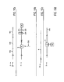
- FIGS. 10a to 10f represent different variants of the usable in the optical assembly 1 invention delay element 8.
- FIG. 10a shows a first configuration in which a delay fiber link 9 is used as a delay element 8, which serves as a dispersion compensation means 39 at the same time.
- two or more fiber types 50a, 50b, 50c of different dispersion properties are coupled together, so that the fiber path 9 overall has effectively zero dispersion.
- so-called IDF fibers 50a (inverse dispersion fiber), DCF fibers 50b (dispersion compensating fiber) and / or SMF fibers 50c (single-mode fiber) can be used in both polarization-preserving and non-polarization-maintaining configurations ,
- FIG. 10b shows a second variant of a delay element 8.
- the primary laser pulses 4 arrive at a pulse divider 5, which is configured as a polarization beam splitter BS.
- a first portion passes directly to an output 50d in the form of primary secondary light pulses 6.
- a second portion passes in the form of second secondary light pulses 7 to a mirror M and from there back to the pulse divider 5, before these second secondary light pulses 7 are also conducted from the pulse divider 5 to the output 50d.
- the delay path here consists of passing through the path between the pulse divider 5 and the mirror M twice.
- This path may comprise both dispersion compensating means 39 and optical elements such as ⁇ / 4 wave paths 50e or Faraday rotators 50f, for the polarization of the second secondary light pulses 7 to influence so that they are possible lossless steered by the pulse divider 5 to the output 50d.
- a dispersion fiber, a photonic crystal fiber, a hollow core fiber or a fiber with reduced nonlinearities is used as the delay fiber path 9 for the delay element 8.
- FIG. 10d shows a variant of the delay element 8, in which a part 7 of the light from the pulse divider 5 is thrown onto a narrow-band mirror, in particular a fiber Bragg grating BG, which reflects the light back onto the pulse divider 5. There, these light pulses 7 together with the pulse divider 5 unhindered continuous beam portions 6 are directed to the output 50 d.
- a narrow-band mirror in particular a fiber Bragg grating BG, which reflects the light back onto the pulse divider 5.
- these light pulses 7 together with the pulse divider 5 unhindered continuous beam portions 6 are directed to the output 50 d.
- Both in this embodiment, as well as in the Embodiment after FIG. 10b can be used in the delay element 8 optical circulators.
- FIG. 10e shows a further variant of a delay element 8 for the optical arrangement 1 according to the invention.
- an optical fiber leads to a reflection grating, a transmission grating or a prism combination K.
- a group of prisms could simultaneously serve as dispersion compensation means 39.
- FIG. 10f a configuration of an optical assembly 1, in which only in the path of the second secondary light pulse 7, an amplifier 37 is provided.
- This amplifier 37 causes a path length difference for the second secondary light pulses 7 relative to the first secondary light pulses 6 and thus represents the delay element 8.
- FIG. 11 shows an embodiment of the optical assembly 1, in which the second secondary light pulses 7 are merged again after passing through the delay element 8 with the first secondary light pulses 6, before both groups of secondary light pulses 6, 7 are conducted into a common optical amplifier 37.
- This common amplifier 37 is thus adapted to amplify both the first secondary light pulses 6 and the second secondary light pulses 7.
- Opposite the configuration in FIG. 8 This offers the advantage of being able to dispense with one of the two optical amplifiers 38, which makes the optical arrangement 1 less complex and therefore much more robust.
- both the first and the second secondary light pulses 6, 7 reach a polarization beam splitter or circulator 51.
- Signal radiation 52 which passes from the experimental setup 52 back to the circulator 51, is directed from there to a detector 54. From the change in the signal radiation 53 with the change in the time delay between the first and second secondary light pulses 6, 7 conclusions can be drawn on a sample examined.
- the experimental setup 52 may also include a terahertz transmitter and / or a terahertz receiver.
- Polarization-obtained circulators usually include a PBS and ⁇ / 4 wave plates or a Faraday rotator.
- control loops 27 of the configurations described above could also be used independently of the measurement of a drift of the average pulse repetition rate (ie also in the thermally isolated or stabilized design of the optical arrangement) in order to be able to set and control the pulse repetition rate in an ideal manner ,
Landscapes
- Physics & Mathematics (AREA)
- Spectroscopy & Molecular Physics (AREA)
- General Physics & Mathematics (AREA)
- Health & Medical Sciences (AREA)
- Optics & Photonics (AREA)
- Electromagnetism (AREA)
- Analytical Chemistry (AREA)
- Immunology (AREA)
- Life Sciences & Earth Sciences (AREA)
- Chemical & Material Sciences (AREA)
- Pathology (AREA)
- Biochemistry (AREA)
- General Health & Medical Sciences (AREA)
- Nonlinear Science (AREA)
- Nuclear Medicine, Radiotherapy & Molecular Imaging (AREA)
- Condensed Matter Physics & Semiconductors (AREA)
- Toxicology (AREA)
- Engineering & Computer Science (AREA)
- Plasma & Fusion (AREA)
- Lasers (AREA)
- Optical Modulation, Optical Deflection, Nonlinear Optics, Optical Demodulation, Optical Logic Elements (AREA)
Applications Claiming Priority (1)
| Application Number | Priority Date | Filing Date | Title |
|---|---|---|---|
| DE102012001357A DE102012001357A1 (de) | 2012-01-24 | 2012-01-24 | Optikanordnung und Verfahren zum Erzeugen von Lichtimpulsen veränderbarer Verzögerung |
Publications (3)
| Publication Number | Publication Date |
|---|---|
| EP2621031A2 true EP2621031A2 (fr) | 2013-07-31 |
| EP2621031A3 EP2621031A3 (fr) | 2018-04-04 |
| EP2621031B1 EP2621031B1 (fr) | 2019-07-31 |
Family
ID=47632776
Family Applications (1)
| Application Number | Title | Priority Date | Filing Date |
|---|---|---|---|
| EP13000268.6A Active EP2621031B1 (fr) | 2012-01-24 | 2013-01-18 | Agencement optique et procédé destinés à générer des impulsions lumineuses à décélération variable |
Country Status (3)
| Country | Link |
|---|---|
| US (1) | US8737439B2 (fr) |
| EP (1) | EP2621031B1 (fr) |
| DE (1) | DE102012001357A1 (fr) |
Cited By (1)
| Publication number | Priority date | Publication date | Assignee | Title |
|---|---|---|---|---|
| EP3139153A1 (fr) * | 2015-09-02 | 2017-03-08 | Philipps-Universität Marburg | Procede et dispositif pour la spectroscopie a dimension temporelle |
Families Citing this family (13)
| Publication number | Priority date | Publication date | Assignee | Title |
|---|---|---|---|---|
| DE102011111114A1 (de) * | 2011-08-19 | 2013-02-21 | Deutsches Elektronen-Synchrotron Desy | System und Verfahren zum Erzeugen eines Synchronisationssteuersignals |
| FR3006068B1 (fr) * | 2013-05-24 | 2015-04-24 | Saint Gobain | Procede d'obtention d'un substrat |
| EP3103166B1 (fr) * | 2014-02-03 | 2022-03-16 | IPG Photonics Corporation | Laser à fibre à impulsions ultracourtes de forte puissance |
| WO2016086310A1 (fr) | 2014-12-04 | 2016-06-09 | Hifi Engineering Inc. | Interrogateur optique permettant de réaliser une interférométrie au moyen de réseaux de bragg sur fibre |
| JP6363511B2 (ja) * | 2015-01-08 | 2018-07-25 | 浜松ホトニクス株式会社 | テラヘルツ波時間波形取得装置 |
| US9494810B2 (en) * | 2015-03-24 | 2016-11-15 | Finisar Corporation | Automatic bias stabilization of dual-polarization in-phase and quadrature optical modulator |
| JP6679959B2 (ja) * | 2016-02-02 | 2020-04-15 | セイコーエプソン株式会社 | 分光測定装置、及び分光測定方法 |
| JP2017168742A (ja) * | 2016-03-17 | 2017-09-21 | 株式会社リコー | レーザー光発生装置 |
| CA3234213A1 (fr) | 2017-06-08 | 2018-12-08 | Hifi Engineering Inc. | Interrogateur optique servant a realiser l'interferometrie au moyen de reseaux de bragg a fibre |
| CN107768977B (zh) * | 2017-11-17 | 2023-06-30 | 中国工程物理研究院流体物理研究所 | 一种基于双光束调制的量子级联激光器的脉冲调控系统 |
| CN111509541B (zh) * | 2020-05-19 | 2021-04-23 | 宝宇(武汉)激光技术有限公司 | 一种时延平衡链路及锁相方法 |
| DE102020003064A1 (de) | 2020-05-24 | 2021-12-09 | Edgewave Gmbh | Lasersysteme mit erhöhter Pulswiederholrate und modifiziertem Pulsprofil |
| DE102021124471A1 (de) | 2021-09-22 | 2023-03-23 | Ruhr-Universität Bochum, Körperschaft des öffentlichen Rechts | Verfahren und Vorrichtung zum Erzeugen einer Lichtpulsabfolge |
Citations (2)
| Publication number | Priority date | Publication date | Assignee | Title |
|---|---|---|---|---|
| US5778016A (en) | 1994-04-01 | 1998-07-07 | Imra America, Inc. | Scanning temporal ultrafast delay methods and apparatuses therefor |
| DE102008026484A1 (de) | 2008-06-03 | 2009-12-10 | Skz - Kfe Ggmbh Kunststoff-Forschung Und -Entwicklung | Verfahren zum Erzeugen zweier optischer Pulse mit variablem, zeitlichem Pulsabstand |
Family Cites Families (6)
| Publication number | Priority date | Publication date | Assignee | Title |
|---|---|---|---|---|
| JPH09101208A (ja) * | 1995-10-03 | 1997-04-15 | Oyo Koden Kenkiyuushitsu:Kk | 光サンプリング波形観測方法および光サンプリング波形観測装置 |
| DE19620594A1 (de) * | 1996-05-22 | 1997-11-27 | Sel Alcatel Ag | Resonator für elektromagnetische Wellen mit einer Stabilisierungseinrichtung und Verfahren zum Stabilisieren der Resonatorlänge |
| US8120778B2 (en) * | 2009-03-06 | 2012-02-21 | Imra America, Inc. | Optical scanning and imaging systems based on dual pulsed laser systems |
| WO2007112449A2 (fr) * | 2006-03-28 | 2007-10-04 | The Regents Of The University Of California | Dispositif et procédé de spectroscopie raman et microscopie par analyse spectrale dans le domaine temporel |
| US8314391B2 (en) * | 2007-12-31 | 2012-11-20 | Honeywell Asca Inc. | Controlling the bends in a fiber optic cable to eliminate measurement error in a scanning terahertz sensor |
| US8379295B2 (en) * | 2010-01-14 | 2013-02-19 | Finisar Corporation | Optical differential phase-shift keyed signal demodulator |
-
2012
- 2012-01-24 DE DE102012001357A patent/DE102012001357A1/de not_active Withdrawn
-
2013
- 2013-01-18 EP EP13000268.6A patent/EP2621031B1/fr active Active
- 2013-01-23 US US13/748,026 patent/US8737439B2/en active Active
Patent Citations (2)
| Publication number | Priority date | Publication date | Assignee | Title |
|---|---|---|---|---|
| US5778016A (en) | 1994-04-01 | 1998-07-07 | Imra America, Inc. | Scanning temporal ultrafast delay methods and apparatuses therefor |
| DE102008026484A1 (de) | 2008-06-03 | 2009-12-10 | Skz - Kfe Ggmbh Kunststoff-Forschung Und -Entwicklung | Verfahren zum Erzeugen zweier optischer Pulse mit variablem, zeitlichem Pulsabstand |
Non-Patent Citations (2)
| Title |
|---|
| R. WILK; T. HOCHREIN; M. KOCH; M. MEI; R. HOLZWARTH: "OSCAT: Novel Technique for Time-Resolved Experiments Without Moveable Optical Delay Lines", J INFRARED MILLI TERAHZ WAVES, vol. 32, 2011, pages 596 - 602 |
| T. HOCHREIN; R. WILK; M. MEI; R. HOLZWARTH; N. KRUMBHOLZ; M. KOCH: "Optical sampling by laser cavity tuning", OPTICS EXPRESS, vol. 18, no. 2, January 2010 (2010-01-01), pages 1613 |
Cited By (2)
| Publication number | Priority date | Publication date | Assignee | Title |
|---|---|---|---|---|
| EP3139153A1 (fr) * | 2015-09-02 | 2017-03-08 | Philipps-Universität Marburg | Procede et dispositif pour la spectroscopie a dimension temporelle |
| WO2017037195A1 (fr) * | 2015-09-02 | 2017-03-09 | Philipps-Universität Marburg | Procédé et dispositif de spectroscopie dans le domaine temporel des téraherz |
Also Published As
| Publication number | Publication date |
|---|---|
| US20130188661A1 (en) | 2013-07-25 |
| EP2621031A3 (fr) | 2018-04-04 |
| EP2621031B1 (fr) | 2019-07-31 |
| DE102012001357A1 (de) | 2013-07-25 |
| US8737439B2 (en) | 2014-05-27 |
Similar Documents
| Publication | Publication Date | Title |
|---|---|---|
| EP2621031B1 (fr) | Agencement optique et procédé destinés à générer des impulsions lumineuses à décélération variable | |
| DE102014226973B4 (de) | Optische Resonatoranordnung und Verfahren zum Einstellen einer Umlaufzeit in einem Resonator | |
| DE112010006131B3 (de) | Optische Abtast- und Abbildsysteme, die auf dualgepulsten Lasersystemen basieren | |
| EP2364106B1 (fr) | Source lumineuse réglable en longueur d'onde | |
| EP3120428B1 (fr) | Procédé pour faire fonctionner un dispositif laser, dispositif résonateur et utilisation d'un déphaseur | |
| DE102015108602B4 (de) | Optische Abtastung | |
| WO2010063051A1 (fr) | Procédé et dispositif pour produire un peigne de fréquences optique autoréférencé | |
| DE112011103954T5 (de) | Frequenzkamm-Quelle mit großem Abstand der Kammlinien | |
| EP3440514B1 (fr) | Methode et appareil pour generer une frequence de reference | |
| EP2901529B1 (fr) | Procédé et dispositif de détermination de la position temporelle relative d'impulsions électromagnétiques | |
| DE202008009021U1 (de) | Elektronisch gesteuerte optische Abtastung | |
| DE102011122232A1 (de) | System zum Erzeugen eines Schwebungssignals | |
| DE102016122047B3 (de) | Erzeugung von Ausgangslaserimpulsen mit einer abstimmbaren Zentralwellenlänge | |
| DE102008045359B3 (de) | Detektion von Veränderungen eines Zeitabstands optischer oder elektrischer Signale | |
| DE102012023605B4 (de) | Verfahren und Vorrichtung zur Synthese von elektromagnetischer Strahlung | |
| DE102015113355B4 (de) | Optische Abtastung | |
| DE102019129337B4 (de) | Laservorrichtung zur Erzeugung eines optischen Frequenzkamms | |
| DE102015200668B4 (de) | Verfahren und System zum Erzeugen eines Treibersignals für ein akusto-optisches Bauelement zur Carrier-Envelope-Phasenstabilisierung | |
| DE102023116866B4 (de) | Verfahren zur Frequenzstabilisierung eines gütegeschalteten schmalbandigen Lasers und dafür ausgebildete Laseranordnung | |
| DE102023103793B3 (de) | Verfahren zur Frequenzstabilisierung eines gütegeschalteten schmalbandigen Lasers und Laseranordnung zur Durchführung des Verfahrens | |
| DE102012008456B4 (de) | Frequenzstabilisierte optische Lichtquelle und Verfahren zur Frequenzstabilisierung von Licht | |
| DE102011012749B4 (de) | Verfahren zum Erzeugen eines Frequenzkamms aus einer Mehrzahl an Kammlinien und Vorrichtung dazu | |
| DE102016107501B3 (de) | Wellenlängenmessvorrichtung und Verfahren zur Messung der Wellenlänge | |
| DE19937565A1 (de) | Verfahren zum Regeln der Ausgangsleistung eines Laserstrahls sowie eine dazugehörige Vorrichtung | |
| EP3890124A1 (fr) | Procédé et dispositif de génération d'un faisceau utile électromagnétique |
Legal Events
| Date | Code | Title | Description |
|---|---|---|---|
| PUAI | Public reference made under article 153(3) epc to a published international application that has entered the european phase |
Free format text: ORIGINAL CODE: 0009012 |
|
| AK | Designated contracting states |
Kind code of ref document: A2 Designated state(s): AL AT BE BG CH CY CZ DE DK EE ES FI FR GB GR HR HU IE IS IT LI LT LU LV MC MK MT NL NO PL PT RO RS SE SI SK SM TR |
|
| AX | Request for extension of the european patent |
Extension state: BA ME |
|
| RIC1 | Information provided on ipc code assigned before grant |
Ipc: G02F 1/37 20060101ALI20171025BHEP Ipc: H01S 3/00 20060101AFI20171025BHEP |
|
| PUAL | Search report despatched |
Free format text: ORIGINAL CODE: 0009013 |
|
| AK | Designated contracting states |
Kind code of ref document: A3 Designated state(s): AL AT BE BG CH CY CZ DE DK EE ES FI FR GB GR HR HU IE IS IT LI LT LU LV MC MK MT NL NO PL PT RO RS SE SI SK SM TR |
|
| AX | Request for extension of the european patent |
Extension state: BA ME |
|
| RIC1 | Information provided on ipc code assigned before grant |
Ipc: H01S 3/00 20060101AFI20180223BHEP Ipc: G02F 1/37 20060101ALI20180223BHEP |
|
| STAA | Information on the status of an ep patent application or granted ep patent |
Free format text: STATUS: REQUEST FOR EXAMINATION WAS MADE |
|
| 17P | Request for examination filed |
Effective date: 20180911 |
|
| RBV | Designated contracting states (corrected) |
Designated state(s): AL AT BE BG CH CY CZ DE DK EE ES FI FR GB GR HR HU IE IS IT LI LT LU LV MC MK MT NL NO PL PT RO RS SE SI SK SM TR |
|
| GRAP | Despatch of communication of intention to grant a patent |
Free format text: ORIGINAL CODE: EPIDOSNIGR1 |
|
| STAA | Information on the status of an ep patent application or granted ep patent |
Free format text: STATUS: GRANT OF PATENT IS INTENDED |
|
| INTG | Intention to grant announced |
Effective date: 20190221 |
|
| GRAS | Grant fee paid |
Free format text: ORIGINAL CODE: EPIDOSNIGR3 |
|
| GRAA | (expected) grant |
Free format text: ORIGINAL CODE: 0009210 |
|
| STAA | Information on the status of an ep patent application or granted ep patent |
Free format text: STATUS: THE PATENT HAS BEEN GRANTED |
|
| AK | Designated contracting states |
Kind code of ref document: B1 Designated state(s): AL AT BE BG CH CY CZ DE DK EE ES FI FR GB GR HR HU IE IS IT LI LT LU LV MC MK MT NL NO PL PT RO RS SE SI SK SM TR |
|
| REG | Reference to a national code |
Ref country code: CH Ref legal event code: EP Ref country code: GB Ref legal event code: FG4D Free format text: NOT ENGLISH |
|
| REG | Reference to a national code |
Ref country code: AT Ref legal event code: REF Ref document number: 1161937 Country of ref document: AT Kind code of ref document: T Effective date: 20190815 |
|
| REG | Reference to a national code |
Ref country code: IE Ref legal event code: FG4D Free format text: LANGUAGE OF EP DOCUMENT: GERMAN |
|
| REG | Reference to a national code |
Ref country code: DE Ref legal event code: R096 Ref document number: 502013013243 Country of ref document: DE |
|
| REG | Reference to a national code |
Ref country code: NL Ref legal event code: MP Effective date: 20190731 |
|
| REG | Reference to a national code |
Ref country code: LT Ref legal event code: MG4D |
|
| PG25 | Lapsed in a contracting state [announced via postgrant information from national office to epo] |
Ref country code: NO Free format text: LAPSE BECAUSE OF FAILURE TO SUBMIT A TRANSLATION OF THE DESCRIPTION OR TO PAY THE FEE WITHIN THE PRESCRIBED TIME-LIMIT Effective date: 20191031 Ref country code: SE Free format text: LAPSE BECAUSE OF FAILURE TO SUBMIT A TRANSLATION OF THE DESCRIPTION OR TO PAY THE FEE WITHIN THE PRESCRIBED TIME-LIMIT Effective date: 20190731 Ref country code: BG Free format text: LAPSE BECAUSE OF FAILURE TO SUBMIT A TRANSLATION OF THE DESCRIPTION OR TO PAY THE FEE WITHIN THE PRESCRIBED TIME-LIMIT Effective date: 20191031 Ref country code: NL Free format text: LAPSE BECAUSE OF FAILURE TO SUBMIT A TRANSLATION OF THE DESCRIPTION OR TO PAY THE FEE WITHIN THE PRESCRIBED TIME-LIMIT Effective date: 20190731 Ref country code: FI Free format text: LAPSE BECAUSE OF FAILURE TO SUBMIT A TRANSLATION OF THE DESCRIPTION OR TO PAY THE FEE WITHIN THE PRESCRIBED TIME-LIMIT Effective date: 20190731 Ref country code: PT Free format text: LAPSE BECAUSE OF FAILURE TO SUBMIT A TRANSLATION OF THE DESCRIPTION OR TO PAY THE FEE WITHIN THE PRESCRIBED TIME-LIMIT Effective date: 20191202 Ref country code: LT Free format text: LAPSE BECAUSE OF FAILURE TO SUBMIT A TRANSLATION OF THE DESCRIPTION OR TO PAY THE FEE WITHIN THE PRESCRIBED TIME-LIMIT Effective date: 20190731 Ref country code: HR Free format text: LAPSE BECAUSE OF FAILURE TO SUBMIT A TRANSLATION OF THE DESCRIPTION OR TO PAY THE FEE WITHIN THE PRESCRIBED TIME-LIMIT Effective date: 20190731 |
|
| PG25 | Lapsed in a contracting state [announced via postgrant information from national office to epo] |
Ref country code: ES Free format text: LAPSE BECAUSE OF FAILURE TO SUBMIT A TRANSLATION OF THE DESCRIPTION OR TO PAY THE FEE WITHIN THE PRESCRIBED TIME-LIMIT Effective date: 20190731 Ref country code: GR Free format text: LAPSE BECAUSE OF FAILURE TO SUBMIT A TRANSLATION OF THE DESCRIPTION OR TO PAY THE FEE WITHIN THE PRESCRIBED TIME-LIMIT Effective date: 20191101 Ref country code: RS Free format text: LAPSE BECAUSE OF FAILURE TO SUBMIT A TRANSLATION OF THE DESCRIPTION OR TO PAY THE FEE WITHIN THE PRESCRIBED TIME-LIMIT Effective date: 20190731 Ref country code: AL Free format text: LAPSE BECAUSE OF FAILURE TO SUBMIT A TRANSLATION OF THE DESCRIPTION OR TO PAY THE FEE WITHIN THE PRESCRIBED TIME-LIMIT Effective date: 20190731 Ref country code: LV Free format text: LAPSE BECAUSE OF FAILURE TO SUBMIT A TRANSLATION OF THE DESCRIPTION OR TO PAY THE FEE WITHIN THE PRESCRIBED TIME-LIMIT Effective date: 20190731 Ref country code: IS Free format text: LAPSE BECAUSE OF FAILURE TO SUBMIT A TRANSLATION OF THE DESCRIPTION OR TO PAY THE FEE WITHIN THE PRESCRIBED TIME-LIMIT Effective date: 20191130 |
|
| PG25 | Lapsed in a contracting state [announced via postgrant information from national office to epo] |
Ref country code: TR Free format text: LAPSE BECAUSE OF FAILURE TO SUBMIT A TRANSLATION OF THE DESCRIPTION OR TO PAY THE FEE WITHIN THE PRESCRIBED TIME-LIMIT Effective date: 20190731 |
|
| PG25 | Lapsed in a contracting state [announced via postgrant information from national office to epo] |
Ref country code: PL Free format text: LAPSE BECAUSE OF FAILURE TO SUBMIT A TRANSLATION OF THE DESCRIPTION OR TO PAY THE FEE WITHIN THE PRESCRIBED TIME-LIMIT Effective date: 20190731 Ref country code: DK Free format text: LAPSE BECAUSE OF FAILURE TO SUBMIT A TRANSLATION OF THE DESCRIPTION OR TO PAY THE FEE WITHIN THE PRESCRIBED TIME-LIMIT Effective date: 20190731 Ref country code: IT Free format text: LAPSE BECAUSE OF FAILURE TO SUBMIT A TRANSLATION OF THE DESCRIPTION OR TO PAY THE FEE WITHIN THE PRESCRIBED TIME-LIMIT Effective date: 20190731 Ref country code: RO Free format text: LAPSE BECAUSE OF FAILURE TO SUBMIT A TRANSLATION OF THE DESCRIPTION OR TO PAY THE FEE WITHIN THE PRESCRIBED TIME-LIMIT Effective date: 20190731 Ref country code: EE Free format text: LAPSE BECAUSE OF FAILURE TO SUBMIT A TRANSLATION OF THE DESCRIPTION OR TO PAY THE FEE WITHIN THE PRESCRIBED TIME-LIMIT Effective date: 20190731 |
|
| PG25 | Lapsed in a contracting state [announced via postgrant information from national office to epo] |
Ref country code: IS Free format text: LAPSE BECAUSE OF FAILURE TO SUBMIT A TRANSLATION OF THE DESCRIPTION OR TO PAY THE FEE WITHIN THE PRESCRIBED TIME-LIMIT Effective date: 20200224 Ref country code: SM Free format text: LAPSE BECAUSE OF FAILURE TO SUBMIT A TRANSLATION OF THE DESCRIPTION OR TO PAY THE FEE WITHIN THE PRESCRIBED TIME-LIMIT Effective date: 20190731 Ref country code: CZ Free format text: LAPSE BECAUSE OF FAILURE TO SUBMIT A TRANSLATION OF THE DESCRIPTION OR TO PAY THE FEE WITHIN THE PRESCRIBED TIME-LIMIT Effective date: 20190731 Ref country code: SK Free format text: LAPSE BECAUSE OF FAILURE TO SUBMIT A TRANSLATION OF THE DESCRIPTION OR TO PAY THE FEE WITHIN THE PRESCRIBED TIME-LIMIT Effective date: 20190731 |
|
| REG | Reference to a national code |
Ref country code: DE Ref legal event code: R097 Ref document number: 502013013243 Country of ref document: DE |
|
| PLBE | No opposition filed within time limit |
Free format text: ORIGINAL CODE: 0009261 |
|
| STAA | Information on the status of an ep patent application or granted ep patent |
Free format text: STATUS: NO OPPOSITION FILED WITHIN TIME LIMIT |
|
| PG2D | Information on lapse in contracting state deleted |
Ref country code: IS |
|
| PG25 | Lapsed in a contracting state [announced via postgrant information from national office to epo] |
Ref country code: IS Free format text: LAPSE BECAUSE OF FAILURE TO SUBMIT A TRANSLATION OF THE DESCRIPTION OR TO PAY THE FEE WITHIN THE PRESCRIBED TIME-LIMIT Effective date: 20191030 |
|
| 26N | No opposition filed |
Effective date: 20200603 |
|
| PG25 | Lapsed in a contracting state [announced via postgrant information from national office to epo] |
Ref country code: MC Free format text: LAPSE BECAUSE OF FAILURE TO SUBMIT A TRANSLATION OF THE DESCRIPTION OR TO PAY THE FEE WITHIN THE PRESCRIBED TIME-LIMIT Effective date: 20190731 Ref country code: SI Free format text: LAPSE BECAUSE OF FAILURE TO SUBMIT A TRANSLATION OF THE DESCRIPTION OR TO PAY THE FEE WITHIN THE PRESCRIBED TIME-LIMIT Effective date: 20190731 |
|
| REG | Reference to a national code |
Ref country code: CH Ref legal event code: PL |
|
| REG | Reference to a national code |
Ref country code: BE Ref legal event code: MM Effective date: 20200131 |
|
| PG25 | Lapsed in a contracting state [announced via postgrant information from national office to epo] |
Ref country code: LU Free format text: LAPSE BECAUSE OF NON-PAYMENT OF DUE FEES Effective date: 20200118 |
|
| PG25 | Lapsed in a contracting state [announced via postgrant information from national office to epo] |
Ref country code: BE Free format text: LAPSE BECAUSE OF NON-PAYMENT OF DUE FEES Effective date: 20200131 Ref country code: CH Free format text: LAPSE BECAUSE OF NON-PAYMENT OF DUE FEES Effective date: 20200131 Ref country code: LI Free format text: LAPSE BECAUSE OF NON-PAYMENT OF DUE FEES Effective date: 20200131 |
|
| PG25 | Lapsed in a contracting state [announced via postgrant information from national office to epo] |
Ref country code: IE Free format text: LAPSE BECAUSE OF NON-PAYMENT OF DUE FEES Effective date: 20200118 |
|
| REG | Reference to a national code |
Ref country code: AT Ref legal event code: MM01 Ref document number: 1161937 Country of ref document: AT Kind code of ref document: T Effective date: 20200118 |
|
| PG25 | Lapsed in a contracting state [announced via postgrant information from national office to epo] |
Ref country code: AT Free format text: LAPSE BECAUSE OF NON-PAYMENT OF DUE FEES Effective date: 20200118 |
|
| PG25 | Lapsed in a contracting state [announced via postgrant information from national office to epo] |
Ref country code: MT Free format text: LAPSE BECAUSE OF FAILURE TO SUBMIT A TRANSLATION OF THE DESCRIPTION OR TO PAY THE FEE WITHIN THE PRESCRIBED TIME-LIMIT Effective date: 20190731 Ref country code: CY Free format text: LAPSE BECAUSE OF FAILURE TO SUBMIT A TRANSLATION OF THE DESCRIPTION OR TO PAY THE FEE WITHIN THE PRESCRIBED TIME-LIMIT Effective date: 20190731 |
|
| PG25 | Lapsed in a contracting state [announced via postgrant information from national office to epo] |
Ref country code: MK Free format text: LAPSE BECAUSE OF FAILURE TO SUBMIT A TRANSLATION OF THE DESCRIPTION OR TO PAY THE FEE WITHIN THE PRESCRIBED TIME-LIMIT Effective date: 20190731 |
|
| PGFP | Annual fee paid to national office [announced via postgrant information from national office to epo] |
Ref country code: GB Payment date: 20260121 Year of fee payment: 14 |
|
| PGFP | Annual fee paid to national office [announced via postgrant information from national office to epo] |
Ref country code: DE Payment date: 20260128 Year of fee payment: 14 |
|
| PGFP | Annual fee paid to national office [announced via postgrant information from national office to epo] |
Ref country code: FR Payment date: 20260123 Year of fee payment: 14 |