EP2622485B1 - Procédé et appareil destinés à réduire la pollution du cache du processeur provoquée par une préanalyse agressive - Google Patents
Procédé et appareil destinés à réduire la pollution du cache du processeur provoquée par une préanalyse agressive Download PDFInfo
- Publication number
- EP2622485B1 EP2622485B1 EP11761810.8A EP11761810A EP2622485B1 EP 2622485 B1 EP2622485 B1 EP 2622485B1 EP 11761810 A EP11761810 A EP 11761810A EP 2622485 B1 EP2622485 B1 EP 2622485B1
- Authority
- EP
- European Patent Office
- Prior art keywords
- cache
- cast out
- entry
- cache entry
- status
- Prior art date
- Legal status (The legal status is an assumption and is not a legal conclusion. Google has not performed a legal analysis and makes no representation as to the accuracy of the status listed.)
- Active
Links
Images


Classifications
-
- G—PHYSICS
- G06—COMPUTING OR CALCULATING; COUNTING
- G06F—ELECTRIC DIGITAL DATA PROCESSING
- G06F12/00—Accessing, addressing or allocating within memory systems or architectures
- G06F12/02—Addressing or allocation; Relocation
- G06F12/08—Addressing or allocation; Relocation in hierarchically structured memory systems, e.g. virtual memory systems
- G06F12/12—Replacement control
- G06F12/121—Replacement control using replacement algorithms
- G06F12/123—Replacement control using replacement algorithms with age lists, e.g. queue, most recently used [MRU] list or least recently used [LRU] list
-
- G—PHYSICS
- G06—COMPUTING OR CALCULATING; COUNTING
- G06F—ELECTRIC DIGITAL DATA PROCESSING
- G06F12/00—Accessing, addressing or allocating within memory systems or architectures
- G06F12/02—Addressing or allocation; Relocation
- G06F12/08—Addressing or allocation; Relocation in hierarchically structured memory systems, e.g. virtual memory systems
- G06F12/12—Replacement control
- G06F12/121—Replacement control using replacement algorithms
- G06F12/128—Replacement control using replacement algorithms adapted to multidimensional cache systems, e.g. set-associative, multicache, multiset or multilevel
-
- G—PHYSICS
- G06—COMPUTING OR CALCULATING; COUNTING
- G06F—ELECTRIC DIGITAL DATA PROCESSING
- G06F12/00—Accessing, addressing or allocating within memory systems or architectures
- G06F12/02—Addressing or allocation; Relocation
- G06F12/08—Addressing or allocation; Relocation in hierarchically structured memory systems, e.g. virtual memory systems
- G06F12/0802—Addressing of a memory level in which the access to the desired data or data block requires associative addressing means, e.g. caches
- G06F12/0893—Caches characterised by their organisation or structure
- G06F12/0897—Caches characterised by their organisation or structure with two or more cache hierarchy levels
-
- G—PHYSICS
- G06—COMPUTING OR CALCULATING; COUNTING
- G06F—ELECTRIC DIGITAL DATA PROCESSING
- G06F12/00—Accessing, addressing or allocating within memory systems or architectures
- G06F12/02—Addressing or allocation; Relocation
- G06F12/08—Addressing or allocation; Relocation in hierarchically structured memory systems, e.g. virtual memory systems
- G06F12/0802—Addressing of a memory level in which the access to the desired data or data block requires associative addressing means, e.g. caches
- G06F12/0862—Addressing of a memory level in which the access to the desired data or data block requires associative addressing means, e.g. caches with prefetch
-
- G—PHYSICS
- G06—COMPUTING OR CALCULATING; COUNTING
- G06F—ELECTRIC DIGITAL DATA PROCESSING
- G06F12/00—Accessing, addressing or allocating within memory systems or architectures
- G06F12/02—Addressing or allocation; Relocation
- G06F12/08—Addressing or allocation; Relocation in hierarchically structured memory systems, e.g. virtual memory systems
- G06F12/0802—Addressing of a memory level in which the access to the desired data or data block requires associative addressing means, e.g. caches
- G06F12/0888—Addressing of a memory level in which the access to the desired data or data block requires associative addressing means, e.g. caches using selective caching, e.g. bypass
-
- G—PHYSICS
- G06—COMPUTING OR CALCULATING; COUNTING
- G06F—ELECTRIC DIGITAL DATA PROCESSING
- G06F2212/00—Indexing scheme relating to accessing, addressing or allocation within memory systems or architectures
- G06F2212/10—Providing a specific technical effect
- G06F2212/1016—Performance improvement
- G06F2212/1021—Hit rate improvement
Definitions
- the disclosed subject matter relates generally to cache memory systems and, more particularly, to a multi-level cache memory system that reduces a performance hit associated with wasted cache prefetching.
- Modern microprocessors are much faster than the memory in which the program is stored. That is, the microprocessor can execute instructions at a rate that is faster than the rate at which the instructions can be retrieved from memory, and thus, the program's instructions cannot be read fast enough to keep the microprocessor busy.
- Prefetching the instructions before they are actually needed by the microprocessor is a useful mechanism to overcome the relatively slow response of memory and allow the processor to operate at its substantially higher speed.
- the instruction is prefetched from memory, it is placed in a cache where it may be accessed very quickly when the processor is ready to execute that particular instruction.
- prefetching is that software programs are not always executed in the order that they are stored. In fact, there are many instructions that cause the software program to branch or jump to another location in the program. Thus, accurately predicting when the program will branch or jump to another location can dramatically affect the quality of the prefetching, and consequently, the speed at which the processor can execute the software program. Many mechanisms have been proposed that supposedly enhance the predictions so as to allow more continuous, speedy operation of the processor. However, these predictors have at least one thing in common - they are at least occasionally wrong and instructions are prefectched that are not used by the processor. That is, prefetch algorithms may prove beneficial for some applications but ineffective on others. When prefetched code or data is not consistently and accurately accessed during the execution of the program, a prefetcher can actually hurt the performance of the processor.
- a 'wasted' prefetch is a memory access that causes a cache to be filled with an anticipated instruction(s) but ages out of the cache before it is accessed. Wasted prefetches consume system and memory bandwidth and pollute the processor core's private caches and also shared Chip-Multi-Processor (CMP) caches.
- CMP Chip-Multi-Processor
- US 2007/094450 discloses a computer system cache memory with at least two levels; a higher level cache and a lower level cache to receive cache lines evicted from the higher level cache.
- US 6,578,111 discloses a system and method for handling streaming data in a cache memory system with several cache lines in a cache, in which efficiency is improved by avoiding replacing data that may be needed later.
- Modern prefetchers can be very aggressive in that they prefetch code and data at high rates with a high proportion of wasted prefetches.
- the method comprises receiving a cache entry in the first cache, and identifying the entry as having an untouched status.
- the status of the cache entry is updated in response to receiving a request for at least a portion of the cache entry.
- the cache entry is cast out according to a preselected cache line replacement algorithm, and storage of the cast out cache entry in the second cache is controlled according to the status of the cast out cache entry.
- Controlling storage of the cast out cache entry further comprises storing the cast out cache entry in the second cache in response to the cache entry having an accessed status, and further comprises, in response to the cast at cache entry having an untouched status, either preventing the cast out cache entry from being stored in the second cache, or storing the cast out cache entry in the second cache and identifying the cast out cache entry as being the least recently used entry in the second cache.
- the memory system comprises a first-level cache, a first-level cache controller, a second-level cache, and a second-level cache controller.
- the first-level cache controller is adapted for identifying a received cache entry as having an untouched status, updating the status of the cache entry to accessed in response to receiving a request for at least a portion of the cache entry, and casting out the cache entry according to a preselected cache line replacement algorithm.
- the second-level cache controller is adapted for controlling storage of the cast out cache entry in the second cache according to the status of the cast out cache entry.
- the second level cache controller controls storage of the cast out cache entry by storing the cast out cache entry in the second cache in response to the cast out cache entry having an accessed status, and further controls storage of the cast out cache entry in the second cache by either preventing storage, or by storing the cast out cache entry in the second cache and identifying the cast out cache entry as being the least recently used entry, in response to the cast out cache entry having an untouched status.
- the microprocessor comprises a core, a first-level cache, a first-level cache controller, a second-level cache, and a second-level cache controller.
- the first-level cache controller is adapted for identifying a received cache entry as having an untouched status, updating the status of the cache entry in response to receiving a request for at least a portion of the cache entry from the core, and casting out the cache entry according to a preselected cache line replacement algorithm.
- the second-level cache controller is adapted for controlling storage of the cast out cache entry in the second cache according to the status of the cast out cache entry.
- the second-level cache controller is adapted for controlling storage of the cast out cache entry in the second cache according to the status of the cast out cache entry.
- the second level cache controller controls storage of the cast out cache entry by storing the cast out cache entry in the second cache in response to the cast out cache entry having an accessed status, and further controls storage of the cast out cache entry in the second cache by either preventing storage or by storing the cast out cache entry in the second cache and identifying the cast out cache entry as being the last recently used entry, in response to the cast out cache entry having an untouched status.
- Figure 1 shows a memory hierarchy for a typical multi-processor system consisting of a plurality of cores 106-111. Each core has a dedicated, private L2 processor cache 112-117. Those skilled in the art will appreciate that while the illustrative embodiment is depicted with six cores 106-111 and six L2 caches 112-117, more or fewer cores and caches may be employed without departing from the scope of the instant invention.
- an L3 cache 120 is shared by all the processor cores 106-111 via a System Request Interface 125.
- the L3 cache is a Last Level Cache (LLC), however, those skilled in the art will appreciate that additional levels of cache may be employed without departing from the scope of the instant invention.
- LLC Last Level Cache
- Each of the cores 106-111 has the ability to store software or executable code and data lines in its corresponding L2 cache 112-117.
- a prefetcher unit 200 (see Figure 2 ) associated with each processor core 106-111 also has the ability to retrieve data and code from external memory 105 via the transfer bar (XBAR) 130 before it is actually needed for execution by the cores 106-111 and store the prefetched code and data in the L2 cache 112-117.
- XBAR transfer bar
- One such methodology involves replacing data or code stored in the cache once it has been stored in the cache for a preselected period of time without being accessed. This process is generally known as "aging out.”
- aging out When a line within the L2 cache 112-117 ages out, it is removed or “cast out” of the L2 cache 112-117 as part of a transaction.
- the cast out lines may be referred to as "victim" lines, and when cast out, they are normally not entirely discarded, but are often installed in the next level cache, such as the L3 cache 120 in the instant embodiment.
- Memory accesses from a processor can generally be divided into two categories, those that arise from execution of the program (demand accesses) and those generated by a prefetcher (prefetches).
- prefetches a distinction is made between prefetches and demand accesses when a line of memory is first installed in the processor cache.
- prefetched lines of memory are installed in the L2 cache 112-117 with an "untouched" attribute, status or flag.
- the phrase untouched attribute, status, or flag is intended to mean an indication that a portion of memory, such as a cache block or line, was prefetched and has not yet been accessed or touched by any of the processor cores 106-111.
- the untouched attribute is cleared, which indicates that the line has been accessed by the processor core 106-111.
- the untouched attribute is exported or delivered along with the victim line being cast out of the L2 cache 112-117 via the SRI 125.
- the untouched attribute can be used to control the install policy used by the L3 cache 120 so as to avoid cache pollution in the L3 cache 120.
- victim lines that have the untouched attribute set may not be installed in the L3 cache 120 at all, or they may be installed in a location in the L3 cache 120 that has been identified as a Least Recently Used (LRU) slot.
- LRU Least Recently Used
- the LRU slot is the next cache line to be cast out from the L3 cache in response to a subsequent storage operation to the L3 cache.
- the cache line that has been discarded from the L2 cache 112-117 is at least temporarily retained in the L3 cache 120 in case the core 106-111 decides to access a memory location that is present in the discarded L2 cache line.
- each line 300 in the L2 cache 112-117 typically contains an address (ADDR) tag 305, access state field 310, LRU field 315 and data 320. It may optionally contain ECC code 325 and other attributes 330.
- the untouched attribute 335 can be stored in a variety of locations within the L2 cache 112-117. For example, the untouched attribute 335 can be stored as a standalone attribute, as shown in Figure 3 , or it may be encoded in the access state field 310.
- the state field is typically identified as a Share (S) state.
- the Share state could be replaced with two states, such as: 1) Share Accessed (S.Accessed); and 2) Share Untouched (S.Untouched).
- the access state field 310 of the prefetched cache line may be set as S.Untouched, indicating that the cache line has not yet been accessed by the core 106-111.
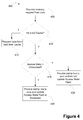
- the core 106-111 when it is executing code, it will send a request to the L2 cache 112-117 for a particular memory address, at block 405. If that memory address has been prefetched into the L2 cache 112-117, the L2 cache 112-117 will detect a "hit” on the prefetched cache line based on the ADDR field 305, at block 410. A "miss" in the L2 cache will be delivered to the L3 cache 120 to determine if the requested memory address is present therein, at block 412.
- the L2 cache 112-117 will inspect the access state field 310, and if the cache line is identified as S.Untouched, the cache line will be sent to the core 106-111 and the cache line in the L2 cache 112-117 will be updated so that the access state field 310 now contains an S.Accessed status, indicating that it has been accessed by the core 106-111. Alternatively, if the cache line is identified as S.Accessed, then at block 425 the cache line will be sent to the core 106-111 and the cache line in the L2 cache 112-117 will not be updated, as its status has already previously been set to to S.Accessed.
- Figure 5 illustrates a flow chart representation of the operation of the L3 cache 120 in response to receiving a line of code from the L2 cache 112-117 during a cast out operation where a line of code has aged out.
- the L3 cache 120 can receive two types of relevant cast outs from the L2 cache 112-117. That is, the L3 cache 120 may be configured to respond differently, depending on whether the access state field 310 is set to S.Accessed or S.Untouched.
- the process begins at decision block 505 with the L3 cache 120 inspecting the access state field 310 of the cast out cache line 300.
- control is passed to block 510 where the L3 cache 120 recognizes that the cast out cache line 300 was never accessed by the core 106-111. Accordingly, in the illustrated embodiment, the untouched, cast out cache line 300 is discarded and not stored in the L3 cache 120 in block 510.
- control is passed to block 515 where the L3 cache 120 recognizes that the cast out cache line 300 was accessed by the core 106-111. Accordingly, in the illustrated embodiment, the accessed, cast out cache line 300 is stored in the L3 cache 120 where it may be quickly and efficiently retrieved if needed.
- FIG. 6 An alternative embodiment of the instant invention is shown in a flow chart representation of the operation of the L3 cache 120 in Figure 6 .
- the operation of the L3 cache 120 is altered to respond differently in the event that the access state field 310 of the cast out cache line 300 is set to S.Untouched, as shown at block 605.
- the L3 cache 120 does not immediately discard the cast out cache line 300, but rather, stores the cast out cache line 300 in the L3 cache 120 despite its access state field 310 having an S.Untouched status. Instead, the L3 cache 120 stores the cast out cache line 300 and identifies it as the LRU entry.
- the L3 cache 120 temporarily stores the untouched, cast out cache line until receiving another cache line, such as a subsequent cast out line from the L2 cache 112-117. That is, because the untouched cache line 300 has been identified as the LRU entry, it has the lowest priority of all the cache lines in the L3 cache 120 and will be the next cache line replaced.
- the instant invention may also find application to instances where data, as opposed to code, is retrieved from memory and placed in the L2 cache 112-117.
- data when data is fetched and stored into a cache, its state field is typically identified as an Exclusive (E) state.
- the Exclusive state could be replaced with two states, such as: 1) Exclusive Accessed (E.Accessed); and 2) Exclusive Untouched (E.Untouched).
- the access state field 310 of the prefetched cache line may be set as E.Untouched, indicating that the cache line has not yet been accessed by the core 106-111.
- the E.Untouched state field will operate in a substantially identical manner as the S.Untouched state field, and the E.Accessed state field will operate in a substantially identical manner as the S.Accessed state field, as described in Figures 4-6 .
- controllers for the L2 and L3 caches that are capable of providing the functionality described in conjunction with Figures 4-6 may be separate stand-alone devices, may be a single device capable of controlling both the L2 and L3 caches, or may be part of a larger device with many more capabilities than those identified with respect to Figures 4-6 .
- HDL hardware descriptive languages
- VLSI circuits very large scale integration circuits
- HDL are VHDL and Verilog/Verilog-XL, but other HDL formats not listed may be used.
- the HDL code e.g., register transfer level (RTL) code/data
- RTL register transfer level
- GDSII data is a descriptive file format and may be used in different embodiments to represent a three-dimensional model of a semiconductor product or device. Such models may be used by semiconductor manufacturing facilities to create semiconductor products and/or devices.
- the GDSII data may be stored as a database or other program storage structure. This data may also be stored on a computer readable storage device (e.g., data storage units, RAM, compact discs, DVDs, solid state storage and the like).
- the GDSII data (or other similar data) may be adapted to configure a manufacturing facility (e.g., through the use of mask works) to create devices capable of embodying various aspects of the instant invention.
- this GDSII data (or other similar data) may be programmed into a computer, processor or controller, which may then control, in whole or part, the operation of a semiconductor manufacturing facility (or fab) to create semiconductor products and devices.
- silicon wafers containing the instant inveniton may be created using the GDSII data (or other similar data).
Landscapes
- Engineering & Computer Science (AREA)
- Theoretical Computer Science (AREA)
- Physics & Mathematics (AREA)
- General Engineering & Computer Science (AREA)
- General Physics & Mathematics (AREA)
- Memory System Of A Hierarchy Structure (AREA)
Claims (5)
- Procédé de commande d'un premier et second cache, comprenant :la réception d'une entrée de cache dans le premier cache (112-117) ;l'identification que l'entrée de cache reçue a un état intact ;la mise à jour de l'état intact de l'entrée de cache vers un état accédé en réponse à la réception d'une demande pour au moins une partie de l'entrée de cache ;l'exclusion de l'entrée de cache selon un algorithme présélectionné de remplacement de ligne de cache ; etla commande de stockage de l'entrée de cache exclue dans le second cache (120) selon un état de l'entrée de cache exclue,caractérisé en ce que la commande du stockage de l'entrée de cache exclue comprend en outre
le stockage de l'entrée de cache exclue dans le second cache en réponse à ce que l'entrée de cache exclue a l'état accédé, et comprend en outre
l'empêchement de stocker l'entrée de cache exclue dans le second cache en réponse à ce que l'entrée de cache exclue a l'état intact. - Procédé de commande d'un premier et second cache, comprenant :la réception d'une entrée de cache dans le premier cache (112-117) ;l'identification que l'entrée de cache reçue a un état intact ;la mise à jour de l'état intact de l'entrée de cache vers un état accédé en réponse à la réception d'une demande pour au moins une partie de l'entrée de cache ;l'exclusion de l'entrée de cache selon un algorithme présélectionné de remplacement de ligne de cache ; etla commande de stockage de l'entrée de cache exclue dans le second cache (120) selon un état de l'entrée de cache exclue,caractérisé en ce que la commande de stockage de l'entrée de cache exclue comprend en outre
le stockage de l'entrée de cache exclue dans le second cache en réponse à ce que l'entrée de cache exclue a l'état accédé, et comprend en outre
le stockage de l'entrée de cache exclue dans le second cache et l'identification que l'entrée de cache exclue est l'entrée la moins récemment utilisée dans le second cache en réponse à ce que l'entrée de cache exclue a un état intact. - Système de mémoire, comprenant :un cache de premier niveau (106-111) ;un cache de second niveau (120) ;un contrôleur de cache de premier niveau adapté pour identifier qu'une entrée de cache reçue a un état intact, pour mettre à jour l'état intact de l'entrée de cache vers un état accédé en réponse à la réception d'une demande pour au moins une partie de l'entrée de cache, et l'exclusion de l'entrée de cache selon un algorithme présélectionné de remplacement de ligne de cache ; etun contrôleur de cache de second niveau adapté pour commander le stockage de l'entrée de cache exclue dans le second cache selon un état de l'entrée de cache exclue, caractérisé en ce quele contrôleur de cache de second niveau commande le stockage de l'entrée de cache exclue en stockant l'entrée de cache exclue dans le second cache en réponse à ce que l'entrée de cache exclue a l'état accédé, et caractérisé en outre en ce que
le contrôleur de cache de second niveau commande le stockage de l'entrée de cache exclue en empêchant que l'entrée de cache exclue soit stockée dans le second cache en réponse à ce que l'entrée de cache exclue a l'état intact. - Système de mémoire, comprenant :un cache de premier niveau (106-111) ;un cache de second niveau (120) ;un contrôleur de cache de premier niveau adapté pour identifier une entrée de cache reçue ayant un état intact, mettre à jour l'état intact de l'entrée de cache vers un état accédé en réponse à la réception d'une demande pour au moins une partie de l'entrée de cache, et l'exclusion de l'entrée de cache selon un algorithme présélectionné de remplacement de ligne de cache ; etun contrôleur de cache de second niveau adapté pour commander le stockage de l'entrée de cache exclue dans le second cache selon un état de l'entrée de cache exclue, caractérisé en ce quele contrôleur de cache de second niveau commande le stockage de l'entrée de cache exclue en stockant l'entrée de cache exclue dans le second cache en réponse à ce que l'entrée de cache exclue a l'état accédé, et caractérisé en outre en ce que
le contrôleur de cache de second niveau commande le stockage de l'entrée de cache exclue en stockant l'entrée de cache exclue dans le second cache et en identifiant que l'entrée de cache exclue est l'entrée la moins récemment utilisée dans le second cache en réponse à ce que l'entrée de cache exclue a l'état intact. - Système de mémoire, selon la revendication 3 ou la revendication 4, dans lequel le contrôleur de cache de premier niveau est adapté pour délivrer l'état de l'entrée de cache exclue au contrôleur de cache de second niveau en réponse à ce que l'entrée de cache est exclue du cache de premier niveau.
Applications Claiming Priority (2)
| Application Number | Priority Date | Filing Date | Title |
|---|---|---|---|
| US12/891,027 US8478942B2 (en) | 2010-09-27 | 2010-09-27 | Method and apparatus for reducing processor cache pollution caused by aggressive prefetching |
| PCT/US2011/052680 WO2012047526A1 (fr) | 2010-09-27 | 2011-09-22 | Procédé et appareil destinés à réduire la pollution du cache du processeur provoquée par une préanalyse agressive |
Publications (2)
| Publication Number | Publication Date |
|---|---|
| EP2622485A1 EP2622485A1 (fr) | 2013-08-07 |
| EP2622485B1 true EP2622485B1 (fr) | 2016-10-26 |
Family
ID=44720194
Family Applications (1)
| Application Number | Title | Priority Date | Filing Date |
|---|---|---|---|
| EP11761810.8A Active EP2622485B1 (fr) | 2010-09-27 | 2011-09-22 | Procédé et appareil destinés à réduire la pollution du cache du processeur provoquée par une préanalyse agressive |
Country Status (6)
| Country | Link |
|---|---|
| US (1) | US8478942B2 (fr) |
| EP (1) | EP2622485B1 (fr) |
| JP (1) | JP5913324B2 (fr) |
| KR (1) | KR101731006B1 (fr) |
| CN (1) | CN103221930B (fr) |
| WO (1) | WO2012047526A1 (fr) |
Cited By (1)
| Publication number | Priority date | Publication date | Assignee | Title |
|---|---|---|---|---|
| WO2019028092A1 (fr) * | 2017-08-03 | 2019-02-07 | Micron Technology, Inc. | Filtre de mémoire cache |
Families Citing this family (3)
| Publication number | Priority date | Publication date | Assignee | Title |
|---|---|---|---|---|
| US9971693B2 (en) * | 2015-05-13 | 2018-05-15 | Ampere Computing Llc | Prefetch tag for eviction promotion |
| US9928176B2 (en) * | 2016-07-20 | 2018-03-27 | Advanced Micro Devices, Inc. | Selecting cache transfer policy for prefetched data based on cache test regions |
| CN110535875B (zh) * | 2019-09-19 | 2021-05-11 | 大连理工大学 | 车载内容中心网络下基于协作方式的缓存污染攻击检测方法 |
Family Cites Families (9)
| Publication number | Priority date | Publication date | Assignee | Title |
|---|---|---|---|---|
| US5603004A (en) * | 1994-02-14 | 1997-02-11 | Hewlett-Packard Company | Method for decreasing time penalty resulting from a cache miss in a multi-level cache system |
| US6578111B1 (en) | 2000-09-29 | 2003-06-10 | Sun Microsystems, Inc. | Cache memory system and method for managing streaming-data |
| JP2005522773A (ja) * | 2002-04-08 | 2005-07-28 | ユニバーシティー・オブ・テキサス・システム | 非均等型キャッシュ装置、システム及び方法 |
| US7133975B1 (en) * | 2003-01-21 | 2006-11-07 | Advanced Micro Devices, Inc. | Cache memory system including a cache memory employing a tag including associated touch bits |
| US7373466B1 (en) * | 2004-04-07 | 2008-05-13 | Advanced Micro Devices, Inc. | Method and apparatus for filtering memory write snoop activity in a distributed shared memory computer |
| US20060069876A1 (en) * | 2004-09-30 | 2006-03-30 | Sorav Bansal | Method and system of clock with adaptive cache replacement and temporal filtering |
| CN1746865A (zh) * | 2005-10-13 | 2006-03-15 | 上海交通大学 | 数字信号处理器可重构指令高速缓存部分的实现方法 |
| US20070094450A1 (en) | 2005-10-26 | 2007-04-26 | International Business Machines Corporation | Multi-level cache architecture having a selective victim cache |
| GB0603552D0 (en) * | 2006-02-22 | 2006-04-05 | Advanced Risc Mach Ltd | Cache management within a data processing apparatus |
-
2010
- 2010-09-27 US US12/891,027 patent/US8478942B2/en active Active
-
2011
- 2011-09-22 KR KR1020137007711A patent/KR101731006B1/ko active Active
- 2011-09-22 WO PCT/US2011/052680 patent/WO2012047526A1/fr not_active Ceased
- 2011-09-22 JP JP2013531661A patent/JP5913324B2/ja active Active
- 2011-09-22 CN CN201180056385.8A patent/CN103221930B/zh active Active
- 2011-09-22 EP EP11761810.8A patent/EP2622485B1/fr active Active
Cited By (3)
| Publication number | Priority date | Publication date | Assignee | Title |
|---|---|---|---|---|
| WO2019028092A1 (fr) * | 2017-08-03 | 2019-02-07 | Micron Technology, Inc. | Filtre de mémoire cache |
| US11366762B2 (en) | 2017-08-03 | 2022-06-21 | Micron Technology, Inc. | Cache filter |
| US11853224B2 (en) | 2017-08-03 | 2023-12-26 | Micron Technology, Inc. | Cache filter |
Also Published As
| Publication number | Publication date |
|---|---|
| EP2622485A1 (fr) | 2013-08-07 |
| KR20130113440A (ko) | 2013-10-15 |
| US8478942B2 (en) | 2013-07-02 |
| JP5913324B2 (ja) | 2016-04-27 |
| US20120079205A1 (en) | 2012-03-29 |
| KR101731006B1 (ko) | 2017-04-27 |
| JP2013542511A (ja) | 2013-11-21 |
| CN103221930A (zh) | 2013-07-24 |
| WO2012047526A1 (fr) | 2012-04-12 |
| CN103221930B (zh) | 2016-09-07 |
Similar Documents
| Publication | Publication Date | Title |
|---|---|---|
| EP2778932B1 (fr) | Dispositifs de prélecture communicants dans un microprocesseur | |
| TWI574155B (zh) | 資料預取方法、電腦程式產品以及微處理器 | |
| US8583894B2 (en) | Hybrid prefetch method and apparatus | |
| US9286223B2 (en) | Merging demand load requests with prefetch load requests | |
| US9483406B2 (en) | Communicating prefetchers that throttle one another | |
| US20100011198A1 (en) | Microprocessor with multiple operating modes dynamically configurable by a device driver based on currently running applications | |
| CN104636270A (zh) | 数据处理装置中的自适应预取 | |
| US8856451B2 (en) | Method and apparatus for adapting aggressiveness of a pre-fetcher | |
| JP4045296B2 (ja) | キャッシュメモリ及びその制御方法 | |
| US11853220B2 (en) | Prefetcher training | |
| US12530301B2 (en) | Prefetch attribute value prediction | |
| EP2622485B1 (fr) | Procédé et appareil destinés à réduire la pollution du cache du processeur provoquée par une préanalyse agressive | |
| JP6701380B2 (ja) | アップ/ダウンプリフェッチャ | |
| US11940921B2 (en) | Bounding box prefetcher | |
| US12585468B2 (en) | Apparatus and method using hint capability for controlling micro-architectural control function | |
| US12013784B2 (en) | Prefetch state cache (PSC) | |
| US11907722B2 (en) | Methods and apparatus for storing prefetch metadata | |
| CN105354010B (zh) | 处理器及由处理器执行硬件数据的方法 | |
| US20240095034A1 (en) | Selective control flow predictor insertion | |
| CN104809080A (zh) | 相互节流的通信预取器 |
Legal Events
| Date | Code | Title | Description |
|---|---|---|---|
| PUAI | Public reference made under article 153(3) epc to a published international application that has entered the european phase |
Free format text: ORIGINAL CODE: 0009012 |
|
| 17P | Request for examination filed |
Effective date: 20130404 |
|
| AK | Designated contracting states |
Kind code of ref document: A1 Designated state(s): AL AT BE BG CH CY CZ DE DK EE ES FI FR GB GR HR HU IE IS IT LI LT LU LV MC MK MT NL NO PL PT RO RS SE SI SK SM TR |
|
| DAX | Request for extension of the european patent (deleted) | ||
| 17Q | First examination report despatched |
Effective date: 20141029 |
|
| GRAP | Despatch of communication of intention to grant a patent |
Free format text: ORIGINAL CODE: EPIDOSNIGR1 |
|
| INTG | Intention to grant announced |
Effective date: 20160704 |
|
| GRAS | Grant fee paid |
Free format text: ORIGINAL CODE: EPIDOSNIGR3 |
|
| GRAA | (expected) grant |
Free format text: ORIGINAL CODE: 0009210 |
|
| AK | Designated contracting states |
Kind code of ref document: B1 Designated state(s): AL AT BE BG CH CY CZ DE DK EE ES FI FR GB GR HR HU IE IS IT LI LT LU LV MC MK MT NL NO PL PT RO RS SE SI SK SM TR |
|
| REG | Reference to a national code |
Ref country code: GB Ref legal event code: FG4D |
|
| REG | Reference to a national code |
Ref country code: CH Ref legal event code: EP |
|
| REG | Reference to a national code |
Ref country code: AT Ref legal event code: REF Ref document number: 840486 Country of ref document: AT Kind code of ref document: T Effective date: 20161115 |
|
| REG | Reference to a national code |
Ref country code: IE Ref legal event code: FG4D |
|
| REG | Reference to a national code |
Ref country code: DE Ref legal event code: R096 Ref document number: 602011031696 Country of ref document: DE |
|
| REG | Reference to a national code |
Ref country code: LT Ref legal event code: MG4D |
|
| PG25 | Lapsed in a contracting state [announced via postgrant information from national office to epo] |
Ref country code: LV Free format text: LAPSE BECAUSE OF FAILURE TO SUBMIT A TRANSLATION OF THE DESCRIPTION OR TO PAY THE FEE WITHIN THE PRESCRIBED TIME-LIMIT Effective date: 20161026 |
|
| REG | Reference to a national code |
Ref country code: NL Ref legal event code: MP Effective date: 20161026 |
|
| REG | Reference to a national code |
Ref country code: AT Ref legal event code: MK05 Ref document number: 840486 Country of ref document: AT Kind code of ref document: T Effective date: 20161026 |
|
| PG25 | Lapsed in a contracting state [announced via postgrant information from national office to epo] |
Ref country code: LT Free format text: LAPSE BECAUSE OF FAILURE TO SUBMIT A TRANSLATION OF THE DESCRIPTION OR TO PAY THE FEE WITHIN THE PRESCRIBED TIME-LIMIT Effective date: 20161026 Ref country code: SE Free format text: LAPSE BECAUSE OF FAILURE TO SUBMIT A TRANSLATION OF THE DESCRIPTION OR TO PAY THE FEE WITHIN THE PRESCRIBED TIME-LIMIT Effective date: 20161026 Ref country code: GR Free format text: LAPSE BECAUSE OF FAILURE TO SUBMIT A TRANSLATION OF THE DESCRIPTION OR TO PAY THE FEE WITHIN THE PRESCRIBED TIME-LIMIT Effective date: 20170127 Ref country code: NO Free format text: LAPSE BECAUSE OF FAILURE TO SUBMIT A TRANSLATION OF THE DESCRIPTION OR TO PAY THE FEE WITHIN THE PRESCRIBED TIME-LIMIT Effective date: 20170126 |
|
| PG25 | Lapsed in a contracting state [announced via postgrant information from national office to epo] |
Ref country code: RS Free format text: LAPSE BECAUSE OF FAILURE TO SUBMIT A TRANSLATION OF THE DESCRIPTION OR TO PAY THE FEE WITHIN THE PRESCRIBED TIME-LIMIT Effective date: 20161026 Ref country code: ES Free format text: LAPSE BECAUSE OF FAILURE TO SUBMIT A TRANSLATION OF THE DESCRIPTION OR TO PAY THE FEE WITHIN THE PRESCRIBED TIME-LIMIT Effective date: 20161026 Ref country code: IS Free format text: LAPSE BECAUSE OF FAILURE TO SUBMIT A TRANSLATION OF THE DESCRIPTION OR TO PAY THE FEE WITHIN THE PRESCRIBED TIME-LIMIT Effective date: 20170226 Ref country code: PL Free format text: LAPSE BECAUSE OF FAILURE TO SUBMIT A TRANSLATION OF THE DESCRIPTION OR TO PAY THE FEE WITHIN THE PRESCRIBED TIME-LIMIT Effective date: 20161026 Ref country code: AT Free format text: LAPSE BECAUSE OF FAILURE TO SUBMIT A TRANSLATION OF THE DESCRIPTION OR TO PAY THE FEE WITHIN THE PRESCRIBED TIME-LIMIT Effective date: 20161026 Ref country code: NL Free format text: LAPSE BECAUSE OF FAILURE TO SUBMIT A TRANSLATION OF THE DESCRIPTION OR TO PAY THE FEE WITHIN THE PRESCRIBED TIME-LIMIT Effective date: 20161026 Ref country code: HR Free format text: LAPSE BECAUSE OF FAILURE TO SUBMIT A TRANSLATION OF THE DESCRIPTION OR TO PAY THE FEE WITHIN THE PRESCRIBED TIME-LIMIT Effective date: 20161026 Ref country code: FI Free format text: LAPSE BECAUSE OF FAILURE TO SUBMIT A TRANSLATION OF THE DESCRIPTION OR TO PAY THE FEE WITHIN THE PRESCRIBED TIME-LIMIT Effective date: 20161026 Ref country code: BE Free format text: LAPSE BECAUSE OF FAILURE TO SUBMIT A TRANSLATION OF THE DESCRIPTION OR TO PAY THE FEE WITHIN THE PRESCRIBED TIME-LIMIT Effective date: 20161026 Ref country code: PT Free format text: LAPSE BECAUSE OF FAILURE TO SUBMIT A TRANSLATION OF THE DESCRIPTION OR TO PAY THE FEE WITHIN THE PRESCRIBED TIME-LIMIT Effective date: 20170227 |
|
| REG | Reference to a national code |
Ref country code: DE Ref legal event code: R097 Ref document number: 602011031696 Country of ref document: DE |
|
| PG25 | Lapsed in a contracting state [announced via postgrant information from national office to epo] |
Ref country code: DK Free format text: LAPSE BECAUSE OF FAILURE TO SUBMIT A TRANSLATION OF THE DESCRIPTION OR TO PAY THE FEE WITHIN THE PRESCRIBED TIME-LIMIT Effective date: 20161026 Ref country code: EE Free format text: LAPSE BECAUSE OF FAILURE TO SUBMIT A TRANSLATION OF THE DESCRIPTION OR TO PAY THE FEE WITHIN THE PRESCRIBED TIME-LIMIT Effective date: 20161026 Ref country code: SK Free format text: LAPSE BECAUSE OF FAILURE TO SUBMIT A TRANSLATION OF THE DESCRIPTION OR TO PAY THE FEE WITHIN THE PRESCRIBED TIME-LIMIT Effective date: 20161026 Ref country code: CZ Free format text: LAPSE BECAUSE OF FAILURE TO SUBMIT A TRANSLATION OF THE DESCRIPTION OR TO PAY THE FEE WITHIN THE PRESCRIBED TIME-LIMIT Effective date: 20161026 Ref country code: RO Free format text: LAPSE BECAUSE OF FAILURE TO SUBMIT A TRANSLATION OF THE DESCRIPTION OR TO PAY THE FEE WITHIN THE PRESCRIBED TIME-LIMIT Effective date: 20161026 |
|
| PG25 | Lapsed in a contracting state [announced via postgrant information from national office to epo] |
Ref country code: IT Free format text: LAPSE BECAUSE OF FAILURE TO SUBMIT A TRANSLATION OF THE DESCRIPTION OR TO PAY THE FEE WITHIN THE PRESCRIBED TIME-LIMIT Effective date: 20161026 Ref country code: BG Free format text: LAPSE BECAUSE OF FAILURE TO SUBMIT A TRANSLATION OF THE DESCRIPTION OR TO PAY THE FEE WITHIN THE PRESCRIBED TIME-LIMIT Effective date: 20170126 Ref country code: SM Free format text: LAPSE BECAUSE OF FAILURE TO SUBMIT A TRANSLATION OF THE DESCRIPTION OR TO PAY THE FEE WITHIN THE PRESCRIBED TIME-LIMIT Effective date: 20161026 |
|
| PLBE | No opposition filed within time limit |
Free format text: ORIGINAL CODE: 0009261 |
|
| STAA | Information on the status of an ep patent application or granted ep patent |
Free format text: STATUS: NO OPPOSITION FILED WITHIN TIME LIMIT |
|
| 26N | No opposition filed |
Effective date: 20170727 |
|
| PG25 | Lapsed in a contracting state [announced via postgrant information from national office to epo] |
Ref country code: SI Free format text: LAPSE BECAUSE OF FAILURE TO SUBMIT A TRANSLATION OF THE DESCRIPTION OR TO PAY THE FEE WITHIN THE PRESCRIBED TIME-LIMIT Effective date: 20161026 |
|
| REG | Reference to a national code |
Ref country code: CH Ref legal event code: PL |
|
| PG25 | Lapsed in a contracting state [announced via postgrant information from national office to epo] |
Ref country code: MC Free format text: LAPSE BECAUSE OF FAILURE TO SUBMIT A TRANSLATION OF THE DESCRIPTION OR TO PAY THE FEE WITHIN THE PRESCRIBED TIME-LIMIT Effective date: 20161026 |
|
| REG | Reference to a national code |
Ref country code: IE Ref legal event code: MM4A |
|
| PG25 | Lapsed in a contracting state [announced via postgrant information from national office to epo] |
Ref country code: LU Free format text: LAPSE BECAUSE OF NON-PAYMENT OF DUE FEES Effective date: 20170922 |
|
| REG | Reference to a national code |
Ref country code: FR Ref legal event code: ST Effective date: 20180531 |
|
| PG25 | Lapsed in a contracting state [announced via postgrant information from national office to epo] |
Ref country code: LI Free format text: LAPSE BECAUSE OF NON-PAYMENT OF DUE FEES Effective date: 20170930 Ref country code: CH Free format text: LAPSE BECAUSE OF NON-PAYMENT OF DUE FEES Effective date: 20170930 Ref country code: IE Free format text: LAPSE BECAUSE OF NON-PAYMENT OF DUE FEES Effective date: 20170922 |
|
| PG25 | Lapsed in a contracting state [announced via postgrant information from national office to epo] |
Ref country code: FR Free format text: LAPSE BECAUSE OF NON-PAYMENT OF DUE FEES Effective date: 20171002 |
|
| PG25 | Lapsed in a contracting state [announced via postgrant information from national office to epo] |
Ref country code: MT Free format text: LAPSE BECAUSE OF NON-PAYMENT OF DUE FEES Effective date: 20170922 |
|
| PG25 | Lapsed in a contracting state [announced via postgrant information from national office to epo] |
Ref country code: HU Free format text: LAPSE BECAUSE OF FAILURE TO SUBMIT A TRANSLATION OF THE DESCRIPTION OR TO PAY THE FEE WITHIN THE PRESCRIBED TIME-LIMIT; INVALID AB INITIO Effective date: 20110922 |
|
| PG25 | Lapsed in a contracting state [announced via postgrant information from national office to epo] |
Ref country code: CY Free format text: LAPSE BECAUSE OF NON-PAYMENT OF DUE FEES Effective date: 20161026 |
|
| PG25 | Lapsed in a contracting state [announced via postgrant information from national office to epo] |
Ref country code: MK Free format text: LAPSE BECAUSE OF FAILURE TO SUBMIT A TRANSLATION OF THE DESCRIPTION OR TO PAY THE FEE WITHIN THE PRESCRIBED TIME-LIMIT Effective date: 20161026 |
|
| PG25 | Lapsed in a contracting state [announced via postgrant information from national office to epo] |
Ref country code: TR Free format text: LAPSE BECAUSE OF FAILURE TO SUBMIT A TRANSLATION OF THE DESCRIPTION OR TO PAY THE FEE WITHIN THE PRESCRIBED TIME-LIMIT Effective date: 20161026 |
|
| PG25 | Lapsed in a contracting state [announced via postgrant information from national office to epo] |
Ref country code: AL Free format text: LAPSE BECAUSE OF FAILURE TO SUBMIT A TRANSLATION OF THE DESCRIPTION OR TO PAY THE FEE WITHIN THE PRESCRIBED TIME-LIMIT Effective date: 20161026 |
|
| P01 | Opt-out of the competence of the unified patent court (upc) registered |
Effective date: 20230530 |
|
| REG | Reference to a national code |
Ref country code: GB Ref legal event code: 732E Free format text: REGISTERED BETWEEN 20241121 AND 20241127 |
|
| REG | Reference to a national code |
Ref country code: DE Ref legal event code: R082 Ref document number: 602011031696 Country of ref document: DE Representative=s name: PETERREINS SCHLEY PATENT- UND RECHTSANWAELTE P, DE Ref country code: DE Ref legal event code: R081 Ref document number: 602011031696 Country of ref document: DE Owner name: ONESTA IP, LLC (N.D.GES.D.STAATES DELAWARE), W, US Free format text: FORMER OWNER: ADVANCED MICRO DEVICES, INC., SUNNYVALE, CALIF., US |
|
| PGFP | Annual fee paid to national office [announced via postgrant information from national office to epo] |
Ref country code: DE Payment date: 20250929 Year of fee payment: 15 |
|
| PGFP | Annual fee paid to national office [announced via postgrant information from national office to epo] |
Ref country code: GB Payment date: 20250905 Year of fee payment: 15 |