EP2624511B1 - Récepteur de signalisation d'amplitude multiniveau - Google Patents
Récepteur de signalisation d'amplitude multiniveau Download PDFInfo
- Publication number
- EP2624511B1 EP2624511B1 EP13150806.1A EP13150806A EP2624511B1 EP 2624511 B1 EP2624511 B1 EP 2624511B1 EP 13150806 A EP13150806 A EP 13150806A EP 2624511 B1 EP2624511 B1 EP 2624511B1
- Authority
- EP
- European Patent Office
- Prior art keywords
- signal
- level
- amplitude
- circuit
- resistor ladder
- Prior art date
- Legal status (The legal status is an assumption and is not a legal conclusion. Google has not performed a legal analysis and makes no representation as to the accuracy of the status listed.)
- Active
Links
Images






Classifications
-
- H—ELECTRICITY
- H04—ELECTRIC COMMUNICATION TECHNIQUE
- H04L—TRANSMISSION OF DIGITAL INFORMATION, e.g. TELEGRAPHIC COMMUNICATION
- H04L25/00—Baseband systems
- H04L25/38—Synchronous or start-stop systems, e.g. for Baudot code
- H04L25/40—Transmitting circuits; Receiving circuits
- H04L25/49—Transmitting circuits; Receiving circuits using code conversion at the transmitter; using predistortion; using insertion of idle bits for obtaining a desired frequency spectrum; using three or more amplitude levels ; Baseband coding techniques specific to data transmission systems
- H04L25/4917—Transmitting circuits; Receiving circuits using code conversion at the transmitter; using predistortion; using insertion of idle bits for obtaining a desired frequency spectrum; using three or more amplitude levels ; Baseband coding techniques specific to data transmission systems using multilevel codes
-
- H—ELECTRICITY
- H03—ELECTRONIC CIRCUITRY
- H03D—DEMODULATION OR TRANSFERENCE OF MODULATION FROM ONE CARRIER TO ANOTHER
- H03D1/00—Demodulation of amplitude-modulated oscillations
-
- H—ELECTRICITY
- H04—ELECTRIC COMMUNICATION TECHNIQUE
- H04L—TRANSMISSION OF DIGITAL INFORMATION, e.g. TELEGRAPHIC COMMUNICATION
- H04L25/00—Baseband systems
- H04L25/02—Details ; arrangements for supplying electrical power along data transmission lines
- H04L25/06—DC level restoring means; Bias distortion correction ; Decision circuits providing symbol by symbol detection
- H04L25/061—DC level restoring means; Bias distortion correction ; Decision circuits providing symbol by symbol detection providing hard decisions only; arrangements for tracking or suppressing unwanted low frequency components, e.g. removal of DC offset
- H04L25/066—Multilevel decisions, not including self-organising maps
-
- H—ELECTRICITY
- H04—ELECTRIC COMMUNICATION TECHNIQUE
- H04L—TRANSMISSION OF DIGITAL INFORMATION, e.g. TELEGRAPHIC COMMUNICATION
- H04L27/00—Modulated-carrier systems
- H04L27/02—Amplitude-modulated carrier systems, e.g. using on-off keying; Single sideband or vestigial sideband modulation
- H04L27/06—Demodulator circuits; Receiver circuits
Definitions
- the present invention relates generally to data communications. More particularly, the present invention relates to circuitry for high-speed data links.
- High-speed data links are used to communicate data between devices in a system.
- Serial interface protocols have been developed at increasingly fast data rates for such high-speed links.
- the data signal for most high-speed serial links use just two voltage levels (amplitudes) to convey information: a high level and a low level.
- the high level may be interpreted as a logical one, and the low level may be interpreted as a logical zero.
- Such signaling is sometimes referred to as "non-return-to-zero" (NRZ) data signaling.
- NRZ signaling one symbol provides one bit of information within one unit interval (Ul).
- multi-level amplitude signaling uses several (at least three) distinct voltage levels.
- Such multi-level amplitude signaling which is sometimes referred to as pulse amplitude modulation (PAM) signaling, communicates more than one bit of information per symbol.
- PAM signaling provides a higher effective data rate than NRZ signaling.
- transceiver complexity generally increases if, instead of NRZ signaling, PAM signaling is implemented.
- a high-speed analog-to-digital converter (ADC) circuit is typically implemented at the front end of the receiver to digitize the PAM signal.
- ADC analog-to-digital converter
- such a high-speed ADC circuit generally requires a relatively large area to implement and typically consumes a large amount of power.
- US 6 173 018 B1 discloses a multi-level comparator for demodulator.
- the demodulator circuit obtaining output data through comparison, made in a four-level comparator and a NRZ comparator, of a signal obtained by subjecting a received signal to a process of detection and predetermined threshold levels, comprises a level detector circuit for detecting the level of the received signal transmitted through the process of detection and a control circuit for controlling relative magnitudes of the level detected in the level detector circuit of the signal transmitted through the process of detection and the predetermined threshold levels for the four-level comparator and the NRZ comparator, whereby stabilized output data conforming to changes in the level of the detected output are made obtainable.
- the receiver circuit includes a peak detector, a reference voltage generator, and a comparator circuit.
- the peak detector is arranged to detect a peak voltage of the multi-level amplitude signal
- the reference voltage generator uses the peak voltage to generate multiple reference voltages.
- the comparator circuit uses the multiple reference voltages to detect an amplitude level of the multi-level amplitude signal.
- Another aspect relates to a method of receiving a multi-level amplitude signal which includes at least three amplitude levels for each symbol period.
- a peak voltage of the multi-level amplitude signal is detected, and multiple reference voltages which depend on the peak voltage are generated.
- the multi-level amplitude signal is compared against the plurality of reference voltages to detect an amplitude level.
- the receiver includes at least a peak detector, a reference voltage generator, and a comparator circuit
- the peak detector is arranged to detect a peak voltage of a transmitted pulse amplitude modulation signal which includes at least three amplitude levels for each symbol period.
- the reference voltage generator is arranged to generate a plurality of reference voltages which depend on the peak voltage.
- the comparator circuit is arranged to compare the pulse amplitude modulation signal against the plurality of reference voltages to detect an amplitude level.
- the present disclosure provides an innovative receiver architecture for PAM signaling that substantially reduces the receiver complexity.
- the receiver architecture automatically aligns a number of slicing voltage levels to minimize the number of required samplers.
- FIG. 1 is a high-level diagram of a communication link 100 in accordance with an embodiment of the invention.
- a communication link 100 is generally composed of a transmitter (TX) 120, a receiver (RX) 140, and a communication channel 130 that is used to communicate signals between the transmitter and the receiver.
- the channel 130 may include one or more lanes.
- the communication link 100 may utilize multi-level signaling to increase the effective data rate of the link 100.
- multi-level signaling uses three or more voltage levels to communicate information.
- PAM-M signaling refers to PAM signaling where the amplitude of each signal pulse may be at one of M voltage levels.
- the amplitude of each signal pulse may be at one of three voltage levels, such as, for instance: -3 volts; 0 volts; or +3 volts.
- the amplitude of each signal pulse may be at one of four voltage levels, such as, for instance: -3 volts; -1 volt; + 1 volt; or +3 volts.
- NRZ signaling is essentially PAM-2 signaling. Note that, while embodiments involving PAM-3 and PAM-4 signaling are described in detail below, the receiver architecture disclosed herein may be applied in general to PAM-M signaling, where M is three or more.
- FIG. 2 is a block diagram depicting a PAM-3 signaling receiver 200 in accordance with an embodiment of the invention.
- the receiver 200 may include a receiver buffer (RX Buffer) 201, an equalizer and automatic gain control (EQ+AGC) circuit 202, a peak detector 204, a voltage reference generator (Vref generator) 206, a 2-comparator circuit 208, a decoder 210, and a deserializer 212.
- RX Buffer receiver buffer
- EQ+AGC equalizer and automatic gain control
- Vref generator voltage reference generator
- decoder 210
- deserializer 212 deserializer
- the RX Buffer 201 may be arranged to receive a PAM-3 signal which has been transmitted over a communication channel 130 and to output a buffered PAM-3 signal (RXI).
- the RXI signal may be input into the EQ+AGC circuit 202. After equalizing and adjusting the gain of the signal, the EQ+AGC circuit 202 may output an equalized and gain-adjusted PAM-3 signal (the RXO signal).
- the RXO signal may be input to both the peak detector 204 and the 2-Comparator circuit 208.
- the peak detector 204 may be arranged to output a peak voltage (Vp) signal which corresponds to a peak voltage of the RXO signal.
- Vp peak voltage
- the peak detector 204 may be implemented, for example, using on-chip signal quality monitoring circuitry which may be referred to as EYE Monitor circuitry.
- the Vp signal may be output to both the Vref generator 206 and the EQ+AGC circuit 202.
- the EQ+AGC circuit 202 may use the Vp signal in its adjustment of the signal gain.
- the Vref generator 206 may be arranged to utilize the Vp signal to generate multiple reference voltage levels. In this case, two reference voltage levels may be generated by the Vref generator 206. One embodiment of the Vref generator 206 is described below in relation to FIG. 3 .
- the 2-comparator circuit 208 may be arranged to use the reference voltage levels from the Vref generator 206 as slicing levels for the PAM-3 signal. A two-bit signal that indicates the comparison results may be output from the 2-comparator circuit 208.
- One embodiment of the 2-comparator circuit 208 is described below in relation to FIG. 4 .
- the 2-bit signal from the 2-comparator circuit 208 may be received by the decoder 210.
- the decoder 210 may be arranged to decode the 2-bit signal so as to re-generate the serial binary data signal from the transmitter.
- the serial binary data signal may be received by the deserializer 212.
- the deserializer 212 may be arranged to convert the serial binary data signal to parallel binary data signals (shown as Data[N:0]).
- the receiver 200 in FIG. 2 does not include an ADC circuit at the front end. Instead, two slicing voltage levels are automatically generated using the peak detector 204 and the Vref generator 206, and the 2-comparator circuit 208 and the decoder 210 are used to demodulate and decode the signal.
- FIG. 3 depicts a reference voltage generator circuit (Vref generator) 300 which may be used by a receiver in accordance with an embodiment of the invention.
- the Vref generator 300 in FIG. 3 may be used as the Vref Generator 206 for the receiver 200 in FIG. 2 .
- the Vref generator 300 may include an inverting amplifier circuit which is formed using a first resistor ladder 302 having an end-to-end resistance R 1 , a second resistor ladder 304 having an end-to-end resistance R 2 , and an operational amplifier (OPA) circuit 306.
- the first resistor ladder 302 may be arranged between a peak voltage Vp input and the negative input terminal of the OPA 306.
- the second resistor ladder 304 may be arranged between the negative input terminal and the output terminal of the OPA 306.
- the positive input terminal of the OPA 306 may be connected to a common mode voltage Vcm.
- the first resistor ladder 302 may include multiple resistor elements R in series, and a first (positive) reference voltage (Vrefp) may be obtained from a node between two adjacent resistor elements R in the ladder.
- the node in the ladder which outputs Vrefp may be programmably selected during configuration of the receiver. In this case, due to the negative terminal of the OPA 306 being effectively driven to Vcm, the voltage level for Vrefp may be programmably selected to be a voltage level in a range between Vp and Vcm.
- the second resistor ladder 304 may also include multiple resistor elements R in series, and a second (negative) reference voltage (Vrefn) may be obtained from a node between two adjacent resistor elements R in the ladder.
- the node in the ladder which outputs Vrefn may be programmably selected during configuration of the receiver.
- the voltage level for Vrefn may be programmably selected to be a voltage level in a range between Vcm and Vo.
- the number of resistor elements may be any number.
- a larger number of resistor elements may be included in a resistor ladder to increase the granularity at which a reference voltage may be programmably selected.
- the resistance of the resistor elements R in a ladder may be the same, or may vary, depending on the implementation.
- FIG. 4 depicts a 2-comparator circuit 400 which may be used by a three-level signaling receiver in accordance with an embodiment of the invention.
- the 2-comparator circuit 400 in FIG. 4 may be used as the 2-comparator circuit 208 for the receiver 200 in FIG. 2 .
- a first comparator 402 may be arranged to compare each symbol in the RXO signal (the equalized and gain-adjusted PAM-3 signal from the EQ + ADC circuit 202) against the Vrefn signal (the negative reference voltage from the Vref generator 206).
- the output of the first comparator 402 may be a first code bit signal B ⁇ 0> which depends on the result of the comparison. For example, B ⁇ 0> may be high (logical one) if RXO is higher than Vrefn at the time of the comparison and may be low (logical zero) if RXO is lower than Vrefn at the time of the comparison.
- a second comparator 404 may be arranged to compare each symbol in the RXO signal against the Vrefp signal (the positive reference voltage from the Vref generator 206).
- the output of the second comparator 404 may be a second code bit signal B ⁇ 1> which depends on the result of the comparison. For example, B ⁇ 1> may be high (logical one) if RXO is higher than Vrefp at the time of the comparison and may be low (logical zero) if RXO is lower than Vrefp at the time of the comparison.
- the two-bit code signal (including B ⁇ 0> and B ⁇ 1>) indicates an amplitude level for each symbol in the PAM-3 signal. For example, if B ⁇ 0> and B ⁇ 1> are both low, then the amplitude may be indicated to be at a low level. If B ⁇ 0> and B ⁇ 1> are both high, then the amplitude may be indicated to be at a high level. Finally, if B ⁇ 0> is high and B ⁇ 1> is low, then the amplitude may be indicated to be at a middle level.
- FIG. 5 shows an example PAM-3 signal (RXO) and two reference levels (Vrefn and Vrefp) that may be generated and used by a receiver circuit in accordance with an embodiment of the invention.
- the RXO signal may transition between three amplitude levels: a low level below Vrefn; a high level above Vrefp; and a middle level between Vrefn and Vrefp.
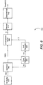
- FIG. 6 is a block diagram depicting a PAM-4 signaling receiver in accordance with an embodiment of the invention.
- the receiver 600 may include a receiver buffer (RX Buffer) 601, an equalizer and automatic gain control (EQ+AGC) circuit 602, a peak detector 604, a voltage reference generator (Vref generator) 606, a 3-comparator circuit 608, a decoder 610, and a deserializer 612.
- RX Buffer receiver buffer
- EQ+AGC equalizer and automatic gain control
- Vref generator voltage reference generator
- the RX Buffer 601 may be arranged to receive a PAM-4 signal which has been transmitted over a communication channel 130 and to output a buffered PAM-4 signal (RXI).
- the RXI signal may be input into the EQ+AGC circuit 602. After equalizing and adjusting the gain of the signal, the EQ+AGC circuit 602 may output an equalized and gain-adjusted PAM-4 signal (the RXO signal).
- the RXO signal may be input to both the peak detector 604 and the 3-Comparator circuit 608.
- the peak detector 604 may be arranged to output a peak voltage (Vp) signal which corresponds to a peak voltage of the RXO signal.
- Vp peak voltage
- the peak detector 604 may be implemented, for example, using EYE Monitor circuitry. As shown, the Vp signal may be output to both the Vref generator 606 and the EQ+AGC circuit 602.
- the EQ+AGC circuit 602 may use the Vp signal in its adjustment of the signal gain.
- the Vref generator 606 may be arranged to utilize the Vp signal to generate multiple reference voltage levels. In this case, two reference voltage levels may be generated by the Vref generator 606. One embodiment of the Vref generator 606 is described above in relation to FIG. 3 .
- the 3-comparator circuit 608 may be arranged to use the two reference voltage levels from the Vref generator 606 and the common mode voltage level (Vcm) as slicing levels for the PAM-4 signal.
- Vcm common mode voltage level
- a three-bit signal that indicates the comparison results may be output from the 3-comparator circuit 608.
- One embodiment of the 3-comparator circuit 608 is described below in relation to FIG. 7 .
- the 3-bit signal from the 3-comparator circuit 608 may be received by the decoder 610.
- the decoder 610 may be arranged to decode the 3-bit signal so as to re-generate the serial binary data signal from the transmitter.
- the serial binary data signal may be received by the deserializer 612.
- the deserializer 612 may be arranged to convert the serial binary data signal to parallel binary data signals (shown as Data[N:0]).
- the receiver 600 in FIG. 6 does not include an ADC circuit at the front end. Instead, three slicing voltage levels are automatically generated using the peak detector 604 and the Vref generator 606, and the 3-comparator circuit 608 and the decoder 610 are used to demodulate and decode the signal.
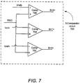
- FIG. 7 depicts a 3-comparator circuit 700 which may be used by a PAM-4 receiver in accordance with an embodiment of the invention.
- the 3-comparator circuit 700 in FIG. 7 may be used as the 3-comparator circuit 608 for the receiver 600 in FIG. 6 .
- a first comparator 702 may be arranged to compare each symbol in the RXO signal (the equalized and gain-adjusted PAM-4 signal from the EQ + ADC circuit 602) against the Vrefn signal (the negative reference voltage from the Vref generator 606).
- the output of the first comparator 702 may be a first code bit signal B ⁇ 0> which depends on the result of the comparison. For example, B ⁇ 0> may be high (logical one) if RXO is higher than Vrefn at the time of the comparison and may be low (logical zero) if RXO is lower than Vrefn at the time of the comparison.
- a second comparator 704 may be arranged to compare each symbol in the RXO signal against the Vcm signal (the common mode voltage).
- the output of the second comparator 704 may be a second code bit signal B ⁇ 1> which depends on the result of the comparison. For example, B ⁇ 1> may be high (logical one) if RXO is higher than Vcm at the time of the comparison and may be low (logical zero) if RXO is lower than Vcm at the time of the comparison.
- a third comparator 706 may be arranged to compare each symbol in the RXO signal against the Vrefp signal (the positive reference voltage from the Vref generator 606).
- the output of the third comparator 704 may be a third code bit signal B ⁇ 2> which depends on the result of the comparison. For example, B ⁇ 2> may be high (logical one) if RXO is higher than Vrefp at the time of the comparison and may be low (logical zero) if RXO is lower than Vrefp at the time of the comparison.
- the three-bit code signal (including B ⁇ 0>, B ⁇ 1>, and B ⁇ 2>) indicates an amplitude level for each symbol in the PAM-4 signal. For example, if B ⁇ 0> is low, then the amplitude may be indicated to be at a lowest level, while if B ⁇ 2> is high, then the amplitude may be indicated to be at a highest level. Else, if B ⁇ 0> is high and B ⁇ 2> is low, then the amplitude may be indicated to be at a second lowest level if B ⁇ 1> is low and may be indicated to be at a second highest level if B ⁇ 1> is high.
- FIG. 8 shows an example PAM-4 signal and three reference levels that may be generated and used by a receiver circuit in accordance with an embodiment of the invention.
- the RXO signal may transition between four amplitude levels: a lowest level below Vrefn; a second lowest level above Vrefn and below Vcm; a second highest level above Vcm and below Vrefp; and a highest level above Vrefp.
- the automatic alignment of the reference levels to slice the PAM-4 signal allows for a minimal number of comparators to be used.
- FIG. 9 shows an example PAM-4 signal and seven reference levels (comp1 through comp7) that may be used by a conventional receiver circuit.
- the reference levels are not automatically aligned to slice the PAM-4 signal. As such, a greater number of comparators are needed to ensure that the reference levels can accurately distinguish between the different levels of the PAM-4 signal.
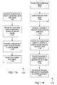
- FIG. 10 is a block diagram of a multi-level amplitude signaling transmitter 1000, while FIG. 11A shows a flow chart of a method of transmitting a multi-level amplitude signal.
- the transmitter 1000 may include a serializer 1002, a coder 1004, and a driver 1006.
- the serializer 1002 receives parallel data signals (DATA[N:0]) to be transmitted over a communication channel 130 to a receiver 140.
- the serializer 1002 serializes 1102 the parallel data signal to generate a serial data signal which is output to the coder 1004.
- the coder 1004 may be arranged to encode 1104 the serial data signal so as to generate a plurality of code bit signals.
- the driver 1006 may be arranged to generate 1106 a multi-level amplitude signal based on the code bit signals and transmit 1108 the multi-level amplitude signal via the communication channel 130 to the receiver 140.
- a method of receiving 1150 a multi-level amplitude signal is shown in FIG. 11B in accordance with an embodiment of the invention.
- the mutli-level amplitude signal may be received, and a peak level of the signal may be detected 1154.
- a plurality of reference levels may be generated 1156.
- the reference levels may be generated 1156 in a manner such that they are automatically aligned.
- the alignment is such that the multi-level amplitude signal may be sliced in a robust way into distinct levels.
- the alignment may be achieved automatically by the detection of the peak voltage and by using a reference voltage generator which has been previously programmed to generate slicing voltages that are appropriate for the particular multi-level amplitude signal being received.
- the multi-level amplitude signal may then be converted 1158 to a plurality of code bit signals using the reference levels, and the plurality of code bit signals may be decoded 1160 to generate the serial data signal. Finally, the serial data signal may be de-serialized 1162 to re-generate the parallel data signal which was transmitted.
- FIG. 12 is a simplified partial block diagram of a field programmable gate array (FPGA) 10 that may be arranged or configured to include one or more of the circuits disclosed herein in accordance with an embodiment of the invention.
- FPGA field programmable gate array
- PLDs programmable logic devices
- CPLDs complex programmable logic devices
- PLAs programmable logic arrays
- DSPs digital signal processors
- ASICs application specific integrated circuits
- FPGA 10 includes within its "core" a two-dimensional array of programmable logic array blocks (or LABs) 12 that are interconnected by a network of column and row interconnect conductors of varying length and speed.
- LABs 12 include multiple (e.g., ten) logic elements (or LEs).
- An LE is a programmable logic block that provides for efficient implementation of user defined logic functions.
- An FPGA has numerous logic elements that can be configured to implement various combinatorial and sequential functions. The logic elements have access to a programmable interconnect structure. The programmable interconnect structure can be programmed to interconnect the logic elements in almost any desired configuration.
- FPGA 10 may also include a distributed memory structure including random access memory (RAM) blocks of varying sizes provided throughout the array.
- RAM random access memory
- the RAM blocks include, for example, blocks 14, blocks 16, and block 18. These memory blocks can also include shift registers and FIFO buffers.
- FPGA 10 may further include digital signal processing (DSP) blocks 20 that can implement, for example, multipliers with add or subtract features.
- DSP digital signal processing
- IOEs 22 located, in this example, around the periphery of the chip support numerous single-ended and differential input/output standards. Each IOE 22 is coupled to an external terminal (i.e., a pin) of FPGA 10.
- a transceiver (TX/RX) channel array may be arranged as shown, for example, with each TX/RX channel circuit 30 being coupled to several LABs.
- a TX/RX channel circuit 30 may include, among other circuitry, the receiver circuitry described herein.
- FPGA 10 is described herein for illustrative purposes only and that the present invention can be implemented in many different types of PLDs, FPGAs, and ASICs.
- FIG. 13 is a block diagram of an exemplary digital system 50 that may employ multi-level amplitude signaling in accordance with an embodiment of the invention. As shown, system 50 may include an FPGA as one of several components.
- System 50 may be, for example, a programmed digital computer system, digital signal processing system, specialized digital switching network, or other processing system.
- System 50 may be designed for a wide variety of applications such as telecommunications systems, automotive systems, control systems, consumer electronics, personal computers, Internet communications and networking, and others. Further, system 50 may be provided on a single board, on multiple boards, or within multiple enclosures.
- system 50 includes a processing unit 52, a memory unit 54, and an input/output (I/O) unit 56 interconnected together by one or more buses.
- FPGA 58 is embedded in processing unit 52.
- FPGA 58 may serve many different purposes within the system 50.
- FPGA 58 may, for example, be a logical building block of processing unit 52, supporting its internal and external operations.
- FPGA 58 is programmed to implement the logical functions necessary to carry on its particular role in system operation.
- FPGA 58 can be specially coupled to memory 54 through connection 60 and to I/O unit 56 through connection 62.
- Processing unit 52 may direct data to an appropriate system component for processing or storage, execute a program stored in memory 54, receive and transmit data via I/O unit 56, or other similar function.
- Processing unit 52 may be a central processing unit (CPU), microprocessor, floating point coprocessor, graphics coprocessor, hardware controller, microcontroller, field programmable gate array programmed for use as a controller, network controller, or any type of processor or controller. Furthermore, in many embodiments, there is often no need for a CPU.
- FPGA 58 may control the logical operations of the system.
- FPGA 58 acts as a reconfigurable processor that may be reprogrammed as needed to handle a particular computing task.
- FPGA 58 may itself include an embedded microprocessor.
- Memory unit 54 may be a random access memory (RAM), read only memory (ROM), fixed or flexible disk media, flash memory, tape, or any other storage means, or any combination of these storage means.
Landscapes
- Engineering & Computer Science (AREA)
- Power Engineering (AREA)
- Computer Networks & Wireless Communication (AREA)
- Signal Processing (AREA)
- Physics & Mathematics (AREA)
- Spectroscopy & Molecular Physics (AREA)
- Dc Digital Transmission (AREA)
Claims (15)
- Circuit récepteur de signalisation d'amplitude multiniveau, le circuit récepteur comprenant :un détecteur de crête (204) adapté pour détecter une tension de crête d'un signal d'amplitude multiniveau qui comporte au moins trois niveaux d'amplitude pour chaque période de symbole ;un générateur de tensions de référence (206 ; 300) adapté pour générer une pluralité de tensions de référence au moins partiellement en réponse à la tension de crête ; etun circuit comparateur (208 ; 400 ; 700) adapté pour utiliser la pluralité de tensions de référence pour détecter un niveau d'amplitude du signal d'amplitude multiniveau ;dans lequel le générateur de tension de référence (300) comprend une première échelle de résistances (302) adaptée pour générer une tension de référence positive de la pluralité de tensions de référence et une seconde échelle de résistances (304) adaptée pour générer une tension de référence négative de la pluralité de tensions de référence,caractérisé en ce quele générateur de tensions de référence (300) comporte un circuit amplificateur inverseur formé par la première échelle de résistances (302), la seconde échelle de résistances (304) et un circuit amplificateur opérationnel (306).
- Circuit récepteur selon la revendication 1, dans lequel un nombre de comparateurs dans le circuit comparateur (208 ; 400 ; 700) est inférieur à un nombre de niveaux d'amplitude dans le signal d'amplitude multiniveau.
- Circuit récepteur selon la revendication 1 ou 2, dans lequel le signal d'amplitude multiniveau comprend un signal de modulation d'amplitude d'impulsion qui comporte au moins trois niveaux d'amplitude pour chaque période de symbole.
- Circuit récepteur selon la revendication 3, dans lequel le signal de modulation d'amplitude d'impulsion comprend un signal modulé en amplitude d'impulsions à trois niveaux (PAM-3), et dans lequel le circuit comparateur (400) comprend moins de trois comparateurs (402, 404).
- Circuit récepteur selon la revendication 3, dans lequel le signal de modulation d'amplitude d'impulsion comprend un signal modulé en amplitude d'impulsions à quatre niveaux (PAM-4), et dans lequel le circuit comparateur (700) comprend moins de quatre comparateurs (702, 704, 706).
- Circuit récepteur selon la revendication 1-5, dans lequel le circuit amplificateur opérationnel (306) présente une borne d'entrée négative connectée à la fois à une première extrémité de la première échelle de résistances (302) et à une première extrémité de la seconde échelle de résistances (304).
- Circuit récepteur selon la revendication 6, dans lequel une seconde extrémité de la première échelle de résistances (302) est adaptée pour recevoir la tension de crête et une seconde extrémité de la seconde échelle de résistances (304) est connectée à une borne de sortie du circuit amplificateur opérationnel (306) et dans lequel une borne d'entrée positive du circuit amplificateur opérationnel (306) est de préférence connectée à une tension de mode commun.
- Procédé de réception d'un signal d'amplitude multiniveau, le procédé comprenant :la détection d'une tension de crête d'un signal d'amplitude multiniveau qui comporte au moins trois niveaux d'amplitude pour chaque période de symbole ;la génération d'une pluralité de tensions de référence en réponse au moins partiellement à la tension de crête au moyen d'une première échelle de résistances (302) pour générer une tension de référence positive de la pluralité de tensions de référence et d'une seconde échelle de résistances (304) pour générer une tension de référence négative de la pluralité de tensions de référence ; etla comparaison du signal d'amplitude multiniveau à la pluralité de tensions de référence pour détecter un niveau d'amplitude,le procédé étant caractérisé en ce quela pluralité de tensions de référence est générée par un générateur de tensions de référence (300) qui comprend un circuit amplificateur inverseur formé par la première échelle de résistances (302), la seconde échelle de résistances (304) et un circuit amplificateur opérationnel (306).
- Procédé selon la revendication 8, dans lequel la comparaison est réalisée par un nombre de comparateurs (402, 404 ; 702, 704, 706) qui est inférieur à un nombre de niveaux d'amplitude dans le signal d'amplitude multiniveau.
- Procédé selon la revendication 9, dans lequel le signal d'amplitude multiniveau comprend un signal modulé en amplitude d'impulsions à trois niveaux (PAM-3), et dans lequel la comparaison par le comparateur est réalisée par moins de trois comparateurs.
- Procédé selon la revendication 9, dans lequel le signal d'amplitude multiniveau comprend un signal modulé en amplitude d'impulsions à quatre niveaux (PAM-4), et dans lequel la comparaison est réalisée par moins de quatre comparateurs.
- Procédé selon la revendication 8-11, dans lequel la pluralité de tensions de référence est générée au moyen du circuit amplificateur opérationnel (306) présentant une borne d'entrée négative connectée à la fois à une première extrémité de la première échelle de résistances (302) et à une première extrémité de la seconde échelle de résistances (304).
- Procédé selon la revendication 12, dans lequel une seconde extrémité de la première échelle de résistances (302) est adaptée pour recevoir la tension de crête, une seconde extrémité de la seconde échelle de résistances (304) est connectée à une borne de sortie du circuit amplificateur opérationnel (306), et une borne d'entrée positive du circuit amplificateur opérationnel (306) est de préférence connectée à une tension de mode commun.
- Circuit intégré comprenant :
un circuit récepteur selon l'une quelconque des revendications 1 à 7. - Circuit intégré selon la revendication 14, comprenant en outre :un émetteur (1000) qui comporte un sérialiseur (1002) agencé pour convertir un signal de données parallèle en un signal de données série,un codeur (1004) agencé pour coder le signal de données série de manière à générer une pluralité de bits de code, etun pilote (1006) agencé pour utiliser la pluralité de bits de code pour générer un signal de modulation d'amplitude d'impulsion à transmettre.
Applications Claiming Priority (1)
| Application Number | Priority Date | Filing Date | Title |
|---|---|---|---|
| US13/363,098 US8750406B2 (en) | 2012-01-31 | 2012-01-31 | Multi-level amplitude signaling receiver |
Publications (2)
| Publication Number | Publication Date |
|---|---|
| EP2624511A1 EP2624511A1 (fr) | 2013-08-07 |
| EP2624511B1 true EP2624511B1 (fr) | 2020-02-26 |
Family
ID=47603254
Family Applications (1)
| Application Number | Title | Priority Date | Filing Date |
|---|---|---|---|
| EP13150806.1A Active EP2624511B1 (fr) | 2012-01-31 | 2013-01-10 | Récepteur de signalisation d'amplitude multiniveau |
Country Status (3)
| Country | Link |
|---|---|
| US (1) | US8750406B2 (fr) |
| EP (1) | EP2624511B1 (fr) |
| CN (1) | CN103259512B (fr) |
Families Citing this family (97)
| Publication number | Priority date | Publication date | Assignee | Title |
|---|---|---|---|---|
| US9246713B2 (en) | 2010-05-20 | 2016-01-26 | Kandou Labs, S.A. | Vector signaling with reduced receiver complexity |
| US9985634B2 (en) | 2010-05-20 | 2018-05-29 | Kandou Labs, S.A. | Data-driven voltage regulator |
| US9251873B1 (en) | 2010-05-20 | 2016-02-02 | Kandou Labs, S.A. | Methods and systems for pin-efficient memory controller interface using vector signaling codes for chip-to-chip communications |
| US9124557B2 (en) | 2010-05-20 | 2015-09-01 | Kandou Labs, S.A. | Methods and systems for chip-to-chip communication with reduced simultaneous switching noise |
| US9288082B1 (en) | 2010-05-20 | 2016-03-15 | Kandou Labs, S.A. | Circuits for efficient detection of vector signaling codes for chip-to-chip communication using sums of differences |
| US9077386B1 (en) | 2010-05-20 | 2015-07-07 | Kandou Labs, S.A. | Methods and systems for selection of unions of vector signaling codes for power and pin efficient chip-to-chip communication |
| DE102012102672B4 (de) * | 2012-03-28 | 2016-11-03 | Austriamicrosystems Ag | Empfängerschaltung und Verfahren zum Empfang eines Eingangssignals sowie Lichtmodul mit einer derartigen Empfängerschaltung und Schaltungsanordnung |
| US9268683B1 (en) | 2012-05-14 | 2016-02-23 | Kandou Labs, S.A. | Storage method and apparatus for random access memory using codeword storage |
| WO2014124450A1 (fr) | 2013-02-11 | 2014-08-14 | Kandou Labs, S.A. | Procédés et systèmes pour interface de communication de puce à puce à haut débit |
| CN110166217B (zh) | 2013-04-16 | 2022-05-17 | 康杜实验室公司 | 高带宽通信接口方法和系统 |
| CN105393512B (zh) | 2013-06-25 | 2019-06-28 | 康杜实验室公司 | 具有低接收器复杂度的向量信令 |
| US9806761B1 (en) | 2014-01-31 | 2017-10-31 | Kandou Labs, S.A. | Methods and systems for reduction of nearest-neighbor crosstalk |
| JP6317474B2 (ja) | 2014-02-02 | 2018-04-25 | カンドウ ラボズ ソシエテ アノニム | 制約isi比を用いる低電力チップ間通信の方法および装置 |
| EP3672176B1 (fr) | 2014-02-28 | 2022-05-11 | Kandou Labs, S.A. | Code de signalisation vectorielle avec horloge imbriquée |
| US9509437B2 (en) * | 2014-05-13 | 2016-11-29 | Kandou Labs, S.A. | Vector signaling code with improved noise margin |
| US11240076B2 (en) | 2014-05-13 | 2022-02-01 | Kandou Labs, S.A. | Vector signaling code with improved noise margin |
| US9852806B2 (en) | 2014-06-20 | 2017-12-26 | Kandou Labs, S.A. | System for generating a test pattern to detect and isolate stuck faults for an interface using transition coding |
| US9112550B1 (en) | 2014-06-25 | 2015-08-18 | Kandou Labs, SA | Multilevel driver for high speed chip-to-chip communications |
| US9252997B1 (en) * | 2014-07-10 | 2016-02-02 | Qualcomm Incorporated | Data link power reduction technique using bipolar pulse amplitude modulation |
| CN106797352B (zh) | 2014-07-10 | 2020-04-07 | 康杜实验室公司 | 高信噪特性向量信令码 |
| US9432082B2 (en) | 2014-07-17 | 2016-08-30 | Kandou Labs, S.A. | Bus reversable orthogonal differential vector signaling codes |
| CN106664272B (zh) | 2014-07-21 | 2020-03-27 | 康杜实验室公司 | 从多点通信信道接收数据的方法和装置 |
| US9461862B2 (en) | 2014-08-01 | 2016-10-04 | Kandou Labs, S.A. | Orthogonal differential vector signaling codes with embedded clock |
| US9674014B2 (en) | 2014-10-22 | 2017-06-06 | Kandou Labs, S.A. | Method and apparatus for high speed chip-to-chip communications |
| WO2016099846A1 (fr) | 2014-12-17 | 2016-06-23 | Rambus Inc. | Niveau de référence d'échantillonneur, décalage de courant continu et adaptation de gain afe pour récepteur pam-n |
| US9674009B2 (en) | 2014-12-19 | 2017-06-06 | Rambus Inc. | Receiver with offset calibration |
| EP3314835B1 (fr) | 2015-06-26 | 2020-04-08 | Kandou Labs S.A. | Système de communication à grande vitesse |
| CN105119690B (zh) * | 2015-07-20 | 2018-08-07 | 北方民族大学 | 一种基于n进制进行数字信号传输的方法 |
| US9595495B1 (en) | 2015-09-28 | 2017-03-14 | Altera Corporation | Multi-level signaling for on-package chip-to-chip interconnect through silicon bridge |
| US10055372B2 (en) | 2015-11-25 | 2018-08-21 | Kandou Labs, S.A. | Orthogonal differential vector signaling codes with embedded clock |
| US10365833B2 (en) | 2016-01-22 | 2019-07-30 | Micron Technology, Inc. | Apparatuses and methods for encoding and decoding of signal lines for multi-level communication architectures |
| WO2017132292A1 (fr) | 2016-01-25 | 2017-08-03 | Kandou Labs, S.A. | Circuit d'attaque à échantillonnage de tension à gain haute fréquence amélioré |
| WO2017180122A1 (fr) * | 2016-04-14 | 2017-10-19 | Hewlett Packard Enterprise Development Lp | Récepteurs optiques |
| CN115085727B (zh) | 2016-04-22 | 2026-04-21 | 康杜实验室公司 | 高性能锁相环 |
| WO2017185070A1 (fr) | 2016-04-22 | 2017-10-26 | Kandou Labs, S.A. | Appareil et procédé d'étalonnage destinés à un échantillonneur à gain haute fréquence réglable |
| US10003454B2 (en) | 2016-04-22 | 2018-06-19 | Kandou Labs, S.A. | Sampler with low input kickback |
| CN109313622B (zh) | 2016-04-28 | 2022-04-15 | 康杜实验室公司 | 用于密集路由线组的向量信令码 |
| CN109417521B (zh) | 2016-04-28 | 2022-03-18 | 康杜实验室公司 | 低功率多电平驱动器 |
| US10153591B2 (en) | 2016-04-28 | 2018-12-11 | Kandou Labs, S.A. | Skew-resistant multi-wire channel |
| US9906358B1 (en) | 2016-08-31 | 2018-02-27 | Kandou Labs, S.A. | Lock detector for phase lock loop |
| US10411922B2 (en) | 2016-09-16 | 2019-09-10 | Kandou Labs, S.A. | Data-driven phase detector element for phase locked loops |
| US10200188B2 (en) | 2016-10-21 | 2019-02-05 | Kandou Labs, S.A. | Quadrature and duty cycle error correction in matrix phase lock loop |
| US10372665B2 (en) | 2016-10-24 | 2019-08-06 | Kandou Labs, S.A. | Multiphase data receiver with distributed DFE |
| US10200218B2 (en) | 2016-10-24 | 2019-02-05 | Kandou Labs, S.A. | Multi-stage sampler with increased gain |
| US10212009B2 (en) * | 2017-03-06 | 2019-02-19 | Blackberry Limited | Modulation for a data bit stream |
| US10069663B1 (en) * | 2017-06-27 | 2018-09-04 | Xilinx, Inc. | System and method for device characterization |
| US10116468B1 (en) | 2017-06-28 | 2018-10-30 | Kandou Labs, S.A. | Low power chip-to-chip bidirectional communications |
| US10686583B2 (en) | 2017-07-04 | 2020-06-16 | Kandou Labs, S.A. | Method for measuring and correcting multi-wire skew |
| US10283187B2 (en) | 2017-07-19 | 2019-05-07 | Micron Technology, Inc. | Apparatuses and methods for providing additional drive to multilevel signals representing data |
| WO2019032379A1 (fr) | 2017-08-07 | 2019-02-14 | Rambus Inc. | Co-étalonnage de récepteur/émetteur de niveaux de tension dans des liaisons de modulation d'amplitude d'impulsion |
| US10203226B1 (en) | 2017-08-11 | 2019-02-12 | Kandou Labs, S.A. | Phase interpolation circuit |
| US11403241B2 (en) | 2017-10-02 | 2022-08-02 | Micron Technology, Inc. | Communicating data with stacked memory dies |
| US10355893B2 (en) * | 2017-10-02 | 2019-07-16 | Micron Technology, Inc. | Multiplexing distinct signals on a single pin of a memory device |
| US10725913B2 (en) | 2017-10-02 | 2020-07-28 | Micron Technology, Inc. | Variable modulation scheme for memory device access or operation |
| US10326623B1 (en) | 2017-12-08 | 2019-06-18 | Kandou Labs, S.A. | Methods and systems for providing multi-stage distributed decision feedback equalization |
| US10554380B2 (en) | 2018-01-26 | 2020-02-04 | Kandou Labs, S.A. | Dynamically weighted exclusive or gate having weighted output segments for phase detection and phase interpolation |
| KR102401996B1 (ko) | 2018-05-28 | 2022-05-24 | 삼성전자주식회사 | 타이밍 조절이 가능한 고속 멀티 레벨 신호 수신기를 포함하는 반도체 장치 및 상기 수신기를 포함하는 반도체 테스트 장치 |
| US10742451B2 (en) | 2018-06-12 | 2020-08-11 | Kandou Labs, S.A. | Passive multi-input comparator for orthogonal codes on a multi-wire bus |
| US10931249B2 (en) | 2018-06-12 | 2021-02-23 | Kandou Labs, S.A. | Amplifier with adjustable high-frequency gain using varactor diodes |
| US10181854B1 (en) | 2018-06-15 | 2019-01-15 | Dialog Semiconductor (Uk) Limited | Low power input buffer using flipped gate MOS |
| US10897382B2 (en) | 2018-06-27 | 2021-01-19 | Korea University Research And Business Foundation | Pulse amplitude modulation-3 transceiver and operation method thereof |
| US10997095B2 (en) * | 2018-08-21 | 2021-05-04 | Micron Technology, Inc. | Training procedure for receivers associated with a memory device |
| US10998011B2 (en) | 2018-08-21 | 2021-05-04 | Micron Technology, Inc. | Drive strength calibration for multi-level signaling |
| US11183983B2 (en) | 2018-09-10 | 2021-11-23 | Kandou Labs, S.A. | Programmable continuous time linear equalizer having stabilized high-frequency peaking for controlling operating current of a slicer |
| US10623214B1 (en) | 2018-12-01 | 2020-04-14 | Hcl Technologies Limited | System and method for multi-level amplitude modulation and demodulation |
| CN109740387A (zh) * | 2019-01-04 | 2019-05-10 | 华大半导体有限公司 | 一种用于在线系统编程的方法和高安全电路 |
| US10680634B1 (en) | 2019-04-08 | 2020-06-09 | Kandou Labs, S.A. | Dynamic integration time adjustment of a clocked data sampler using a static analog calibration circuit |
| US10608849B1 (en) | 2019-04-08 | 2020-03-31 | Kandou Labs, S.A. | Variable gain amplifier and sampler offset calibration without clock recovery |
| US10721106B1 (en) | 2019-04-08 | 2020-07-21 | Kandou Labs, S.A. | Adaptive continuous time linear equalization and channel bandwidth control |
| US10574487B1 (en) | 2019-04-08 | 2020-02-25 | Kandou Labs, S.A. | Sampler offset calibration during operation |
| US10623217B1 (en) * | 2019-05-29 | 2020-04-14 | Nvidia Corp. | Proportional AC-coupled edge-boosting transmit equalization for multi-level pulse-amplitude modulated signaling |
| CN110278034A (zh) * | 2019-08-07 | 2019-09-24 | 青岛海信宽带多媒体技术有限公司 | 一种光模块及光接收控制方法 |
| CN110489373B (zh) * | 2019-08-21 | 2021-07-20 | 格威半导体(厦门)有限公司 | 一种串行隔离通信方法、装置及系统 |
| CN113810029B (zh) * | 2020-06-12 | 2025-01-03 | 圣邦微电子(北京)股份有限公司 | 一种检测数据相关性的电路 |
| KR102801426B1 (ko) * | 2020-08-19 | 2025-04-29 | 삼성전자주식회사 | 수신 회로, 이를 포함하는 인쇄 회로 기판 및 인터페이스 회로 |
| KR102835912B1 (ko) | 2020-08-31 | 2025-07-22 | 삼성전자주식회사 | 멀티 레벨 신호 수신기 및 이를 포함하는 메모리 시스템 |
| WO2022100860A1 (fr) * | 2020-11-16 | 2022-05-19 | Huawei Technologies Co., Ltd. | Détection d'un signal optique à modulation d'intensité par un dispositif de réception à bande passante étroite |
| US11454943B2 (en) * | 2020-11-21 | 2022-09-27 | Geo Micro Devices (Xiamen) Co., Ltd | Serial isolation communication method, device and system |
| US11652567B2 (en) | 2020-12-01 | 2023-05-16 | Micron Technology, Inc. | Replacement scheme for a pulse amplitude modulated bus |
| CN112769416B (zh) * | 2020-12-24 | 2023-05-09 | 成都海光微电子技术有限公司 | 信号接收器、集成电路芯片、信号传输系统及电子设备 |
| CN112838847B (zh) * | 2020-12-31 | 2023-05-09 | 成都海光微电子技术有限公司 | 信号接收器、集成电路芯片、信号传输系统及电子设备 |
| US11303484B1 (en) | 2021-04-02 | 2022-04-12 | Kandou Labs SA | Continuous time linear equalization and bandwidth adaptation using asynchronous sampling |
| US11374800B1 (en) | 2021-04-14 | 2022-06-28 | Kandou Labs SA | Continuous time linear equalization and bandwidth adaptation using peak detector |
| US11456708B1 (en) | 2021-04-30 | 2022-09-27 | Kandou Labs SA | Reference generation circuit for maintaining temperature-tracked linearity in amplifier with adjustable high-frequency gain |
| CN114124050B (zh) * | 2021-10-14 | 2025-08-15 | 北京国科天迅科技股份有限公司 | Pam-nrz信号转换电路、转换方法、设备及介质 |
| KR20230056315A (ko) | 2021-10-20 | 2023-04-27 | 삼성전자주식회사 | 멀티 레벨 신호 수신을 위한 수신기 및 이를 포함하는 메모리 장치 |
| US12074738B2 (en) | 2021-11-26 | 2024-08-27 | Samsung Electronics Co., Ltd. | Semiconductor device |
| US11817861B2 (en) | 2021-11-29 | 2023-11-14 | Samsung Electronics Co., Ltd. | Receiver including offset compensation circuit |
| TWI780004B (zh) * | 2022-02-17 | 2022-10-01 | 瑞昱半導體股份有限公司 | 訊號偵測電路以及訊號偵測方法 |
| US12355409B2 (en) | 2022-03-24 | 2025-07-08 | Kandou Labs SA | Variable gain amplifier with cross-coupled common mode reduction |
| EP4270887B1 (fr) * | 2022-04-25 | 2026-02-18 | Samsung Electronics Co., Ltd. | Émetteur et récepteur pour signalisation à modulation d'amplitude d'impulsion à trois niveaux et système les comprenant |
| KR102608463B1 (ko) * | 2023-05-25 | 2023-11-30 | 서울과학기술대학교 산학협력단 | 4단계의 진폭 변조 신호 수신 장치 및 방법 |
| KR20240174377A (ko) | 2023-06-08 | 2024-12-17 | 삼성전자주식회사 | 수신기, 그의 동작 방법, 및 메모리 장치 |
| KR102766806B1 (ko) * | 2023-07-25 | 2025-02-11 | 고려대학교산학협력단 | Pam-4 디코더의 비교기 개수를 최소화한 판정 궤환 등화기 및 그 동작 방법 |
| KR102916810B1 (ko) * | 2024-03-20 | 2026-01-23 | 서울대학교산학협력단 | 단일 종단 신호를 위한 클럭 참조 pam3 송수신기 |
| KR20250147091A (ko) * | 2024-04-03 | 2025-10-13 | 에스케이하이닉스 주식회사 | 수신 회로, 이를 이용하는 반도체 장치 및 반도체 시스템 |
| CN121239164A (zh) * | 2024-06-27 | 2025-12-30 | 集益威半导体(上海)有限公司 | 用于高速串行接收器的前端 |
Family Cites Families (16)
| Publication number | Priority date | Publication date | Assignee | Title |
|---|---|---|---|---|
| US3534273A (en) | 1967-12-18 | 1970-10-13 | Bell Telephone Labor Inc | Automatic threshold level selection and eye tracking in digital transmission systems |
| US5761246A (en) * | 1995-08-14 | 1998-06-02 | International Business Machines Corporation | Circuit for multiplexing a plurality of signals on one transmission line between chips |
| US5832038A (en) | 1996-07-03 | 1998-11-03 | Motorola, Inc. | Method and apparatus for classifying a multi-level signal |
| JPH10163877A (ja) | 1996-11-28 | 1998-06-19 | Sony Corp | 復調回路における多値コンパレータのしきい値制御回路 |
| CN1189037A (zh) * | 1996-11-28 | 1998-07-29 | 索尼公司 | 用于解调器的多级比较器 |
| US6324602B1 (en) | 1998-08-17 | 2001-11-27 | Integrated Memory Logic, Inc. | Advanced input/output interface for an integrated circuit device using two-level to multi-level signal conversion |
| US6198779B1 (en) | 1999-05-05 | 2001-03-06 | Motorola | Method and apparatus for adaptively classifying a multi-level signal |
| CA2296209C (fr) | 2000-01-17 | 2003-04-01 | Philsar Semiconductor Inc. | Methode et appareil de generation dynamique de seuils de decision a niveaux multiples d'un signal code a base m |
| US6771675B1 (en) * | 2000-08-17 | 2004-08-03 | International Business Machines Corporation | Method for facilitating simultaneous multi-directional transmission of multiple signals between multiple circuits using a single transmission line |
| US7386053B2 (en) * | 2002-10-11 | 2008-06-10 | Synopsys, Inc | System and method of equalization of high speed signals |
| US7233164B2 (en) | 2003-12-17 | 2007-06-19 | Rambus Inc. | Offset cancellation in a multi-level signaling system |
| KR100583631B1 (ko) | 2005-09-23 | 2006-05-26 | 주식회사 아나패스 | 클록 신호가 임베딩된 멀티 레벨 시그널링을 사용하는디스플레이, 타이밍 제어부 및 컬럼 구동 집적회로 |
| US8026740B2 (en) | 2008-03-21 | 2011-09-27 | Micron Technology, Inc. | Multi-level signaling for low power, short channel applications |
| US7795915B2 (en) | 2008-08-04 | 2010-09-14 | Chil Semiconductor Corporation | Multi-level signaling |
| CN101989001B (zh) * | 2009-07-30 | 2012-07-04 | 华映视讯(吴江)有限公司 | 液晶显示器的共同电压产生电路 |
| US8594262B2 (en) | 2010-06-17 | 2013-11-26 | Transwitch Corporation | Apparatus and method thereof for clock and data recovery of N-PAM encoded signals using a conventional 2-PAM CDR circuit |
-
2012
- 2012-01-31 US US13/363,098 patent/US8750406B2/en active Active
-
2013
- 2013-01-10 EP EP13150806.1A patent/EP2624511B1/fr active Active
- 2013-01-30 CN CN201310045106.9A patent/CN103259512B/zh active Active
Non-Patent Citations (1)
| Title |
|---|
| None * |
Also Published As
| Publication number | Publication date |
|---|---|
| US8750406B2 (en) | 2014-06-10 |
| US20130195155A1 (en) | 2013-08-01 |
| CN103259512A (zh) | 2013-08-21 |
| EP2624511A1 (fr) | 2013-08-07 |
| CN103259512B (zh) | 2018-04-20 |
Similar Documents
| Publication | Publication Date | Title |
|---|---|---|
| EP2624511B1 (fr) | Récepteur de signalisation d'amplitude multiniveau | |
| KR101949964B1 (ko) | 임베딩된 클록을 갖는 직교 차동 벡터 시그널링 코드 | |
| CN106797352B (zh) | 高信噪特性向量信令码 | |
| US8275030B2 (en) | Signaling system with selectively-inhibited adaptive equalization | |
| US7180957B2 (en) | Technique for utilizing spare bandwidth resulting from the use of a transition-limiting code in a multi-level signaling system | |
| US9049075B2 (en) | Adaptive modal PAM2/PAM4 in-phase (I) quadrature (Q) phase detector for a receiver | |
| KR20160117505A (ko) | 제한된 isi 비율을 갖는 저전력 칩 대 칩 통신을 위한 방법 및 장치 | |
| KR102203390B1 (ko) | 싱글 엔디드 3-레벨 펄스 진폭 변조 시그널링을 위한 장치 및 방법 | |
| US8553752B2 (en) | Method and apparatus for determining a calibration signal | |
| US10270627B2 (en) | Receiver for high speed communication channel | |
| KR102780824B1 (ko) | 고유 하프-레이트 동작으로의 c-phy 데이터-트리거된 에지 생성 | |
| CN104247356A (zh) | 多值信号传输系统 | |
| KR20130043559A (ko) | 이퀄라이저, 이를 포함하는 리시버 회로 및 이퀄라이징 방법 | |
| US20110229152A1 (en) | Bit-Rate Discrimination Method and Its Apparatus | |
| US9923738B1 (en) | Backchannel transmission adaptation | |
| US9998303B1 (en) | Method of adaptively controlling a low frequency equalizer | |
| US20250132767A1 (en) | Dynamic Voltage Scaling for Asynchronous Analog to Digital Converters | |
| US7535964B2 (en) | Self-clocked two-level differential signaling methods and apparatus | |
| US8526532B2 (en) | Transmitter with dynamic equalizer | |
| CN112234953B (zh) | 边沿调制发射器及数字隔离器 | |
| CN115133922A (zh) | 一种pam-4信号电平判决阈值的移位装置及电子设备 | |
| Tang et al. | PWAM signalling scheme for high speed serial link transceiver design | |
| Yuminaka et al. | Multiple-Valued Pulse-Position Modulation Techniques for Efficient Data Transmission |
Legal Events
| Date | Code | Title | Description |
|---|---|---|---|
| PUAI | Public reference made under article 153(3) epc to a published international application that has entered the european phase |
Free format text: ORIGINAL CODE: 0009012 |
|
| AK | Designated contracting states |
Kind code of ref document: A1 Designated state(s): AL AT BE BG CH CY CZ DE DK EE ES FI FR GB GR HR HU IE IS IT LI LT LU LV MC MK MT NL NO PL PT RO RS SE SI SK SM TR |
|
| AX | Request for extension of the european patent |
Extension state: BA ME |
|
| 17P | Request for examination filed |
Effective date: 20131217 |
|
| RBV | Designated contracting states (corrected) |
Designated state(s): AL AT BE BG CH CY CZ DE DK EE ES FI FR GB GR HR HU IE IS IT LI LT LU LV MC MK MT NL NO PL PT RO RS SE SI SK SM TR |
|
| STAA | Information on the status of an ep patent application or granted ep patent |
Free format text: STATUS: EXAMINATION IS IN PROGRESS |
|
| 17Q | First examination report despatched |
Effective date: 20171130 |
|
| GRAP | Despatch of communication of intention to grant a patent |
Free format text: ORIGINAL CODE: EPIDOSNIGR1 |
|
| STAA | Information on the status of an ep patent application or granted ep patent |
Free format text: STATUS: GRANT OF PATENT IS INTENDED |
|
| RIC1 | Information provided on ipc code assigned before grant |
Ipc: H03D 1/00 20060101ALI20190911BHEP Ipc: H04L 27/06 20060101ALI20190911BHEP Ipc: H04L 25/06 20060101ALI20190911BHEP Ipc: H04L 25/49 20060101AFI20190911BHEP |
|
| INTG | Intention to grant announced |
Effective date: 20190930 |
|
| RIN1 | Information on inventor provided before grant (corrected) |
Inventor name: DING, WEIQI Inventor name: SHIMANOUCHI, MASASHI Inventor name: SHUMARAYEV, SERGEY Inventor name: PAN, MINGDE Inventor name: LI, PENG |
|
| GRAS | Grant fee paid |
Free format text: ORIGINAL CODE: EPIDOSNIGR3 |
|
| GRAA | (expected) grant |
Free format text: ORIGINAL CODE: 0009210 |
|
| STAA | Information on the status of an ep patent application or granted ep patent |
Free format text: STATUS: THE PATENT HAS BEEN GRANTED |
|
| AK | Designated contracting states |
Kind code of ref document: B1 Designated state(s): AL AT BE BG CH CY CZ DE DK EE ES FI FR GB GR HR HU IE IS IT LI LT LU LV MC MK MT NL NO PL PT RO RS SE SI SK SM TR |
|
| REG | Reference to a national code |
Ref country code: GB Ref legal event code: FG4D |
|
| REG | Reference to a national code |
Ref country code: CH Ref legal event code: EP |
|
| REG | Reference to a national code |
Ref country code: AT Ref legal event code: REF Ref document number: 1239026 Country of ref document: AT Kind code of ref document: T Effective date: 20200315 |
|
| REG | Reference to a national code |
Ref country code: IE Ref legal event code: FG4D |
|
| REG | Reference to a national code |
Ref country code: DE Ref legal event code: R096 Ref document number: 602013066156 Country of ref document: DE |
|
| PG25 | Lapsed in a contracting state [announced via postgrant information from national office to epo] |
Ref country code: FI Free format text: LAPSE BECAUSE OF FAILURE TO SUBMIT A TRANSLATION OF THE DESCRIPTION OR TO PAY THE FEE WITHIN THE PRESCRIBED TIME-LIMIT Effective date: 20200226 Ref country code: RS Free format text: LAPSE BECAUSE OF FAILURE TO SUBMIT A TRANSLATION OF THE DESCRIPTION OR TO PAY THE FEE WITHIN THE PRESCRIBED TIME-LIMIT Effective date: 20200226 Ref country code: NO Free format text: LAPSE BECAUSE OF FAILURE TO SUBMIT A TRANSLATION OF THE DESCRIPTION OR TO PAY THE FEE WITHIN THE PRESCRIBED TIME-LIMIT Effective date: 20200526 |
|
| REG | Reference to a national code |
Ref country code: NL Ref legal event code: MP Effective date: 20200226 |
|
| REG | Reference to a national code |
Ref country code: LT Ref legal event code: MG4D |
|
| PG25 | Lapsed in a contracting state [announced via postgrant information from national office to epo] |
Ref country code: BG Free format text: LAPSE BECAUSE OF FAILURE TO SUBMIT A TRANSLATION OF THE DESCRIPTION OR TO PAY THE FEE WITHIN THE PRESCRIBED TIME-LIMIT Effective date: 20200526 Ref country code: SE Free format text: LAPSE BECAUSE OF FAILURE TO SUBMIT A TRANSLATION OF THE DESCRIPTION OR TO PAY THE FEE WITHIN THE PRESCRIBED TIME-LIMIT Effective date: 20200226 Ref country code: HR Free format text: LAPSE BECAUSE OF FAILURE TO SUBMIT A TRANSLATION OF THE DESCRIPTION OR TO PAY THE FEE WITHIN THE PRESCRIBED TIME-LIMIT Effective date: 20200226 Ref country code: LV Free format text: LAPSE BECAUSE OF FAILURE TO SUBMIT A TRANSLATION OF THE DESCRIPTION OR TO PAY THE FEE WITHIN THE PRESCRIBED TIME-LIMIT Effective date: 20200226 Ref country code: GR Free format text: LAPSE BECAUSE OF FAILURE TO SUBMIT A TRANSLATION OF THE DESCRIPTION OR TO PAY THE FEE WITHIN THE PRESCRIBED TIME-LIMIT Effective date: 20200527 Ref country code: IS Free format text: LAPSE BECAUSE OF FAILURE TO SUBMIT A TRANSLATION OF THE DESCRIPTION OR TO PAY THE FEE WITHIN THE PRESCRIBED TIME-LIMIT Effective date: 20200626 |
|
| PG25 | Lapsed in a contracting state [announced via postgrant information from national office to epo] |
Ref country code: NL Free format text: LAPSE BECAUSE OF FAILURE TO SUBMIT A TRANSLATION OF THE DESCRIPTION OR TO PAY THE FEE WITHIN THE PRESCRIBED TIME-LIMIT Effective date: 20200226 |
|
| PG25 | Lapsed in a contracting state [announced via postgrant information from national office to epo] |
Ref country code: DK Free format text: LAPSE BECAUSE OF FAILURE TO SUBMIT A TRANSLATION OF THE DESCRIPTION OR TO PAY THE FEE WITHIN THE PRESCRIBED TIME-LIMIT Effective date: 20200226 Ref country code: SM Free format text: LAPSE BECAUSE OF FAILURE TO SUBMIT A TRANSLATION OF THE DESCRIPTION OR TO PAY THE FEE WITHIN THE PRESCRIBED TIME-LIMIT Effective date: 20200226 Ref country code: EE Free format text: LAPSE BECAUSE OF FAILURE TO SUBMIT A TRANSLATION OF THE DESCRIPTION OR TO PAY THE FEE WITHIN THE PRESCRIBED TIME-LIMIT Effective date: 20200226 Ref country code: SK Free format text: LAPSE BECAUSE OF FAILURE TO SUBMIT A TRANSLATION OF THE DESCRIPTION OR TO PAY THE FEE WITHIN THE PRESCRIBED TIME-LIMIT Effective date: 20200226 Ref country code: CZ Free format text: LAPSE BECAUSE OF FAILURE TO SUBMIT A TRANSLATION OF THE DESCRIPTION OR TO PAY THE FEE WITHIN THE PRESCRIBED TIME-LIMIT Effective date: 20200226 Ref country code: RO Free format text: LAPSE BECAUSE OF FAILURE TO SUBMIT A TRANSLATION OF THE DESCRIPTION OR TO PAY THE FEE WITHIN THE PRESCRIBED TIME-LIMIT Effective date: 20200226 Ref country code: PT Free format text: LAPSE BECAUSE OF FAILURE TO SUBMIT A TRANSLATION OF THE DESCRIPTION OR TO PAY THE FEE WITHIN THE PRESCRIBED TIME-LIMIT Effective date: 20200719 Ref country code: ES Free format text: LAPSE BECAUSE OF FAILURE TO SUBMIT A TRANSLATION OF THE DESCRIPTION OR TO PAY THE FEE WITHIN THE PRESCRIBED TIME-LIMIT Effective date: 20200226 Ref country code: LT Free format text: LAPSE BECAUSE OF FAILURE TO SUBMIT A TRANSLATION OF THE DESCRIPTION OR TO PAY THE FEE WITHIN THE PRESCRIBED TIME-LIMIT Effective date: 20200226 |
|
| REG | Reference to a national code |
Ref country code: AT Ref legal event code: MK05 Ref document number: 1239026 Country of ref document: AT Kind code of ref document: T Effective date: 20200226 |
|
| REG | Reference to a national code |
Ref country code: DE Ref legal event code: R097 Ref document number: 602013066156 Country of ref document: DE |
|
| PLBE | No opposition filed within time limit |
Free format text: ORIGINAL CODE: 0009261 |
|
| STAA | Information on the status of an ep patent application or granted ep patent |
Free format text: STATUS: NO OPPOSITION FILED WITHIN TIME LIMIT |
|
| PG25 | Lapsed in a contracting state [announced via postgrant information from national office to epo] |
Ref country code: IT Free format text: LAPSE BECAUSE OF FAILURE TO SUBMIT A TRANSLATION OF THE DESCRIPTION OR TO PAY THE FEE WITHIN THE PRESCRIBED TIME-LIMIT Effective date: 20200226 Ref country code: AT Free format text: LAPSE BECAUSE OF FAILURE TO SUBMIT A TRANSLATION OF THE DESCRIPTION OR TO PAY THE FEE WITHIN THE PRESCRIBED TIME-LIMIT Effective date: 20200226 |
|
| 26N | No opposition filed |
Effective date: 20201127 |
|
| PG25 | Lapsed in a contracting state [announced via postgrant information from national office to epo] |
Ref country code: PL Free format text: LAPSE BECAUSE OF FAILURE TO SUBMIT A TRANSLATION OF THE DESCRIPTION OR TO PAY THE FEE WITHIN THE PRESCRIBED TIME-LIMIT Effective date: 20200226 Ref country code: SI Free format text: LAPSE BECAUSE OF FAILURE TO SUBMIT A TRANSLATION OF THE DESCRIPTION OR TO PAY THE FEE WITHIN THE PRESCRIBED TIME-LIMIT Effective date: 20200226 |
|
| PG25 | Lapsed in a contracting state [announced via postgrant information from national office to epo] |
Ref country code: MC Free format text: LAPSE BECAUSE OF FAILURE TO SUBMIT A TRANSLATION OF THE DESCRIPTION OR TO PAY THE FEE WITHIN THE PRESCRIBED TIME-LIMIT Effective date: 20200226 |
|
| REG | Reference to a national code |
Ref country code: CH Ref legal event code: PL |
|
| PG25 | Lapsed in a contracting state [announced via postgrant information from national office to epo] |
Ref country code: LU Free format text: LAPSE BECAUSE OF NON-PAYMENT OF DUE FEES Effective date: 20210110 |
|
| REG | Reference to a national code |
Ref country code: BE Ref legal event code: MM Effective date: 20210131 |
|
| PG25 | Lapsed in a contracting state [announced via postgrant information from national office to epo] |
Ref country code: FR Free format text: LAPSE BECAUSE OF NON-PAYMENT OF DUE FEES Effective date: 20210131 |
|
| PG25 | Lapsed in a contracting state [announced via postgrant information from national office to epo] |
Ref country code: CH Free format text: LAPSE BECAUSE OF NON-PAYMENT OF DUE FEES Effective date: 20210131 Ref country code: LI Free format text: LAPSE BECAUSE OF NON-PAYMENT OF DUE FEES Effective date: 20210131 |
|
| PG25 | Lapsed in a contracting state [announced via postgrant information from national office to epo] |
Ref country code: IE Free format text: LAPSE BECAUSE OF NON-PAYMENT OF DUE FEES Effective date: 20210110 |
|
| PG25 | Lapsed in a contracting state [announced via postgrant information from national office to epo] |
Ref country code: BE Free format text: LAPSE BECAUSE OF NON-PAYMENT OF DUE FEES Effective date: 20210131 |
|
| PG25 | Lapsed in a contracting state [announced via postgrant information from national office to epo] |
Ref country code: HU Free format text: LAPSE BECAUSE OF FAILURE TO SUBMIT A TRANSLATION OF THE DESCRIPTION OR TO PAY THE FEE WITHIN THE PRESCRIBED TIME-LIMIT; INVALID AB INITIO Effective date: 20130110 |
|
| PG25 | Lapsed in a contracting state [announced via postgrant information from national office to epo] |
Ref country code: CY Free format text: LAPSE BECAUSE OF FAILURE TO SUBMIT A TRANSLATION OF THE DESCRIPTION OR TO PAY THE FEE WITHIN THE PRESCRIBED TIME-LIMIT Effective date: 20200226 |
|
| P01 | Opt-out of the competence of the unified patent court (upc) registered |
Effective date: 20230531 |
|
| PG25 | Lapsed in a contracting state [announced via postgrant information from national office to epo] |
Ref country code: MK Free format text: LAPSE BECAUSE OF FAILURE TO SUBMIT A TRANSLATION OF THE DESCRIPTION OR TO PAY THE FEE WITHIN THE PRESCRIBED TIME-LIMIT Effective date: 20200226 |
|
| PG25 | Lapsed in a contracting state [announced via postgrant information from national office to epo] |
Ref country code: MT Free format text: LAPSE BECAUSE OF FAILURE TO SUBMIT A TRANSLATION OF THE DESCRIPTION OR TO PAY THE FEE WITHIN THE PRESCRIBED TIME-LIMIT Effective date: 20200226 |
|
| PG25 | Lapsed in a contracting state [announced via postgrant information from national office to epo] |
Ref country code: TR Free format text: LAPSE BECAUSE OF FAILURE TO SUBMIT A TRANSLATION OF THE DESCRIPTION OR TO PAY THE FEE WITHIN THE PRESCRIBED TIME-LIMIT Effective date: 20200226 |
|
| PGFP | Annual fee paid to national office [announced via postgrant information from national office to epo] |
Ref country code: GB Payment date: 20251120 Year of fee payment: 14 |
|
| PGFP | Annual fee paid to national office [announced via postgrant information from national office to epo] |
Ref country code: DE Payment date: 20251119 Year of fee payment: 14 |