EP2625731B1 - Lighting element having oled modules - Google Patents
Lighting element having oled modules Download PDFInfo
- Publication number
- EP2625731B1 EP2625731B1 EP11764774.3A EP11764774A EP2625731B1 EP 2625731 B1 EP2625731 B1 EP 2625731B1 EP 11764774 A EP11764774 A EP 11764774A EP 2625731 B1 EP2625731 B1 EP 2625731B1
- Authority
- EP
- European Patent Office
- Prior art keywords
- oled
- region
- oled module
- carrier element
- contact
- Prior art date
- Legal status (The legal status is an assumption and is not a legal conclusion. Google has not performed a legal analysis and makes no representation as to the accuracy of the status listed.)
- Not-in-force
Links
Images


Classifications
-
- H—ELECTRICITY
- H10—SEMICONDUCTOR DEVICES; ELECTRIC SOLID-STATE DEVICES NOT OTHERWISE PROVIDED FOR
- H10K—ORGANIC ELECTRIC SOLID-STATE DEVICES
- H10K59/00—Integrated devices, or assemblies of multiple devices, comprising at least one organic light-emitting element covered by group H10K50/00
- H10K59/80—Constructional details
- H10K59/84—Parallel electrical configurations of multiple OLEDs
-
- H—ELECTRICITY
- H10—SEMICONDUCTOR DEVICES; ELECTRIC SOLID-STATE DEVICES NOT OTHERWISE PROVIDED FOR
- H10K—ORGANIC ELECTRIC SOLID-STATE DEVICES
- H10K50/00—Organic light-emitting devices
- H10K50/80—Constructional details
- H10K50/805—Electrodes
- H10K50/81—Anodes
- H10K50/814—Anodes combined with auxiliary electrodes, e.g. ITO layer combined with metal lines
-
- H—ELECTRICITY
- H10—SEMICONDUCTOR DEVICES; ELECTRIC SOLID-STATE DEVICES NOT OTHERWISE PROVIDED FOR
- H10K—ORGANIC ELECTRIC SOLID-STATE DEVICES
- H10K59/00—Integrated devices, or assemblies of multiple devices, comprising at least one organic light-emitting element covered by group H10K50/00
- H10K59/80—Constructional details
- H10K59/805—Electrodes
- H10K59/8051—Anodes
- H10K59/80516—Anodes combined with auxiliary electrodes, e.g. ITO layer combined with metal lines
-
- F—MECHANICAL ENGINEERING; LIGHTING; HEATING; WEAPONS; BLASTING
- F21—LIGHTING
- F21Y—INDEXING SCHEME ASSOCIATED WITH SUBCLASSES F21K, F21L, F21S and F21V, RELATING TO THE FORM OR THE KIND OF THE LIGHT SOURCES OR OF THE COLOUR OF THE LIGHT EMITTED
- F21Y2105/00—Planar light sources
-
- F—MECHANICAL ENGINEERING; LIGHTING; HEATING; WEAPONS; BLASTING
- F21—LIGHTING
- F21Y—INDEXING SCHEME ASSOCIATED WITH SUBCLASSES F21K, F21L, F21S and F21V, RELATING TO THE FORM OR THE KIND OF THE LIGHT SOURCES OR OF THE COLOUR OF THE LIGHT EMITTED
- F21Y2105/00—Planar light sources
- F21Y2105/10—Planar light sources comprising a two-dimensional [2D] array of point-like light-generating elements
-
- F—MECHANICAL ENGINEERING; LIGHTING; HEATING; WEAPONS; BLASTING
- F21—LIGHTING
- F21Y—INDEXING SCHEME ASSOCIATED WITH SUBCLASSES F21K, F21L, F21S and F21V, RELATING TO THE FORM OR THE KIND OF THE LIGHT SOURCES OR OF THE COLOUR OF THE LIGHT EMITTED
- F21Y2105/00—Planar light sources
- F21Y2105/10—Planar light sources comprising a two-dimensional [2D] array of point-like light-generating elements
- F21Y2105/12—Planar light sources comprising a two-dimensional [2D] array of point-like light-generating elements characterised by the geometrical disposition of the light-generating elements, e.g. arranging light-generating elements in differing patterns or densities
-
- F—MECHANICAL ENGINEERING; LIGHTING; HEATING; WEAPONS; BLASTING
- F21—LIGHTING
- F21Y—INDEXING SCHEME ASSOCIATED WITH SUBCLASSES F21K, F21L, F21S and F21V, RELATING TO THE FORM OR THE KIND OF THE LIGHT SOURCES OR OF THE COLOUR OF THE LIGHT EMITTED
- F21Y2113/00—Combination of light sources
-
- F—MECHANICAL ENGINEERING; LIGHTING; HEATING; WEAPONS; BLASTING
- F21—LIGHTING
- F21Y—INDEXING SCHEME ASSOCIATED WITH SUBCLASSES F21K, F21L, F21S and F21V, RELATING TO THE FORM OR THE KIND OF THE LIGHT SOURCES OR OF THE COLOUR OF THE LIGHT EMITTED
- F21Y2115/00—Light-generating elements of semiconductor light sources
- F21Y2115/10—Light-emitting diodes [LED]
- F21Y2115/15—Organic light-emitting diodes [OLED]
Definitions
- the invention relates to a light-emitting element having a first OLED module (OLED: organic light-emitting diode) and a second OLED module, which are arranged on a carrier element, as well as electrical conductors for the electrical power supply of the two OLED modules. Moreover, the invention relates to a luminaire with such a luminous element.
- OLED organic light-emitting diode
- An OLED can be used to form a light-emitting element with a flat light emission area for diffuse light emission.
- an OLED which has an anode as the first electrode in the form of a transparent ITO layer (ITO: indium tin oxide), a cathode as a second electrode in the form of a metallic layer and one between the anode and the cathode arranged organic layer which serves to generate light.
- ITO indium tin oxide
- the light generated by the organic layer is released through the transparent ITO layer to the outside.
- the anode has a layer thickness of about 100 nm
- the cathode has a layer thickness of about 100 to 500 nm
- the organic layer has a layer thickness of about 100 to 200 nm.
- the organic layer can have several, for example seven, subleaves ,
- An OLED is a current-driven component in which as homogeneous a current density distribution as possible and, associated therewith, a light output that appears as homogeneous as possible are desired.
- the ITO layer has a comparatively high-resistance surface resistance; this can be in the range of 10 to 20 ohms / square.
- a contact region for electrical contacting of the ITO layer is only possible at the edge of the OLED. Therefore, in the case of a comparatively large light output range, inhomogeneity of the power supply occurs, which leads to a visible inhomogeneity of the light output. Consequently
- the area size of the light output range is limited to a maximum of about 50 mm by 50 mm.
- metal grids In order to realize larger radiating surfaces, it is also known to introduce metal reinforcements in the form of nets, so-called “metal grids” or “busbars", into the ITO layer. As a result, the effective sheet resistance can be lowered in accordance with the illumination density, so that larger uniformly luminous light emission areas can be formed.
- these metal reinforcements made of non-translucent material, so that the light output is reduced overall.
- Metal grids are therefore only useful if they occupy a maximum of about 25% of the ITO area. A possible improvement would be to lower the resistance by increasing the thickness of the metal grids; However, this is not meaningful due to structuring options and due to the layer thicknesses of the organic layers.
- a metal-reinforced ITO layer is electrically contacted only at its outer edges, so that despite a reduced resistance even with a Metallgrid the maximum area size of the light emitting area is limited to achieve a homogeneous light output.
- OLED module is referred to in the present case, such a unit.
- an OLED module can have a rectangular or square light-emitting region whose edge lengths are in the range of a few centimeters.
- the invention has for its object to provide a corresponding lighting element that can be easily produced with good lighting properties.
- a lamp should be specified with such a light element.
- a luminous element which has a first OLED module and a second OLED module, and a carrier element, on which the first OLED module and the second OLED module are arranged. Furthermore, the luminous element has electrical conductors for the electrical power supply of the first OLED module and the second OLED module.
- the first OLED module has at least three electrical contact regions for the supply of electrical current
- the second OLED module has at least three further electrical contact regions for the supply of electrical current.
- Each of the contact areas is in each case electrically conductively connected to one of the conductors.
- the electrical conductors are at least partially disposed on the carrier element; In this case, the conductors are arranged on the carrier element such that they do not cross over.
- the at least three contact regions of the first OLED module and the at least three further contact regions of the second OLED module Due to the at least three contact regions of the first OLED module and the at least three further contact regions of the second OLED module, a particularly homogeneous current feed into the two OLED modules and thus a particularly uniform light output of the light module can be achieved; Due to the special, crossing-free arrangement of the electrical conductors on the support element a particularly simple production of the light element is possible. In addition, a particularly uniform optical appearance of the light-emitting element can be achieved if the conductors do not cross over on the carrier element.
- a particularly uniform current feed into the first OLED module can be achieved if the first OLED module is shaped such that it has a first edge region and a second edge region, which lies opposite the first edge region, wherein a first contact region of the three contact regions the first electrode of the first OLED module is electrically connected, a second contact region of the three contact regions is also electrically connected to the first electrode of the first OLED module and the first contact region on the first Edge region is arranged and the second contact region at the second edge region.
- a power supply or current dissipation
- the first OLED module preferably has a rectangular shape, in particular a square shape, wherein the first edge region is given by a first side region of the four side regions defined by the shape, and the second edge region by that further side region which is opposite to the first side region or the first edge region is given by a first corner region defined by the shape, and the second edge region by a further corner region, which is opposite to the first corner region.
- the luminous element also has a plurality of further OLED modules which are likewise arranged on the carrier element, the first OLED module, the second OLED module and the further OLED modules are arranged on the carrier element in such a way that they form rows and columns.
- an arm of a first electrical conductor of the electrical conductors is arranged on the carrier element in a boundary region between two of the columns.
- those of the OLED modules that form one of the two columns are electrically connected in parallel and electrically connected to the arm of the first electrical conductor.
- an arm of a second electrical conductor of the electrical conductors is arranged on the carrier element such that it extends between those OLED modules which form one of the two columns, on the one hand, and the carrier element on the other hand.
- a particularly large light emission area of the luminous element can be advantageously achieved if the first OLED module, the second OLED module and the further OLED modules each have a light emission area that is greater than 1 cm 2 , preferably greater than 4 cm 2 , especially preferably greater than 20 cm 2
- an electrical conductor of the electrical conductors has an at least partially translucent conductor region, which is arranged between the first OLED module and the carrier element.
- a substantially unimpeded light output of the OLED module in two opposite directions is possible.
- the conductor region does not appreciably impair the light output of the luminous element, for example due to scattering at edge regions or edges of the conductor or the like.
- the luminous element is designed in such a way that, viewed in a cross section through the first contact region and the second contact region and the carrier element, an elongated intermediate space is formed between the first OLED module and the carrier element and the conductor region is longer than half, preferably more than 80%, particularly preferably 100% of the longitudinal extent of the intermediate space occupies. In this way, in particular edges of the conductor, which could adversely affect a light output, reliably prevent.
- the OLED modules of that column in which the first OLED module is located are electrically connected in series or in parallel.
- the other columns can be electrically connected in the same way.
- the carrier element is at least partially translucent and consists for example of glass, PMMA (polymethylmethacrylate) or of a film, for example of PET (polyethylene terephthalate) or it is not translucent and consists for example of metal or plastic.
- the three electrical contact areas are preferably each electrically connected to one of the conductors via a conductive adhesive, a soft solder, a flex cable, a terminal contact or a mechanical spring contact.
- the electrical conductors are advantageously formed from a metal, such as aluminum, silver, chromium or copper or a metal alloy, which is or is applied to the carrier element.
- the electrical conductors can advantageously also be formed of a transparent material, for example of ITO or FTO (fluorine-doped tin oxide) or ZnO (zinc oxide) or PEDOT (poly-3,4-ethylenedioxythiophene), which is applied to the carrier element.
- a luminaire in particular for room lighting, which has a luminous element according to the invention.
- the lighting element can advantageously represent the only light source of the lamp.
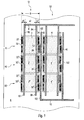
- Fig. 1 is a plan outlined on a first embodiment of a luminous element according to the invention.
- the luminous element has a first OLED module 2 and a second OLED module 4.
- the first OLED module 2 has in particular how already indicated, a first electrode as an anode, a second electrode as a cathode, and arranged between the two electrodes organic layer for light generation.
- the first OLED module 2 may be designed in such a way that it has only the two named electrodes on electrodes, ie no further electrode.
- the first OLED module 2 can furthermore be configured in such a way that the said three layers each extend as far as lateral edge regions of the OLED module 2.
- the first OLED module 2 can be flexible or flexible.
- the second OLED module 4 can be constructed in a corresponding manner.
- the luminous element has a carrier element 6, on which the first OLED module 2 and the second OLED module 4 are arranged.
- the carrier element 6 may be a substantially two-dimensional component, that is, for example, a plate-shaped component, so that two opposite, large flat sides are formed, wherein the two OLED modules 2, 4 are preferably arranged on only one of the two flat sides ,
- the carrier element 6 can be flexible or flexible.
- the two OLED modules 2, 4 may each be mechanically fixed on the support element 6, preferably be mechanically fixed directly, for example via a screw connection and / or an adhesive bond.
- the luminous element has electrical conductors 8, 10, which serve for an electrical power supply of the two OLED modules 2, 4, namely comprising a first conductor 10 and a second conductor 8.
- the first OLED module 2 has three contact areas 22, 24, 26 for the supply of electric current, namely a first contact area 22, a second contact area 24 and a third contact area 26.
- the three contact areas 22, 24, 26 can - as in Fig. 1 indicated - each be designed to be elongated, each extending along a rectilinear edge region of the first OLED module 2.
- Each of the three contact areas 22, 24, 26 can be connected to either Anode or electrically conductively connected to the cathode of the first OLED module 2.
- the second OLED module 4 has three further contact regions 42, 44, 46 for the supply of electric current, which are preferably formed in an analogous manner to the first-mentioned three contact regions 22, 24, 26.
- Each of the contact regions 22, 24, 26, 42, 44, 46 is electrically conductively connected to one of the two electrical conductors 8, 10.
- the first contact region 22 is connected to the second conductor 8, the second contact region 24 likewise to the second conductor 8 and the third contact region 26 to the first conductor 10.
- the first contact region 22 and the second contact region 24 be electrically conductively connected to the anode of the first OLED module 2 and the third contact region 26 with the cathode of the first OLED module 2. This is particularly advantageous if the anode has a comparatively high resistance, as is the case for example the anode is formed of an ITO layer.
- the further contact regions 42 and 44 of the second OLED module 4 are connected to the second conductor 8 and the further contact region 46 to the first conductor 10 in the example shown.
- two of the three contact regions 22, 24, 26 of the first OLED module 2 can be connected to the cathode of the first OLED module 2 and the corresponding third contact region with the anode. The same applies to the second OLED module 4.
- connection between the first contact region 22 and the second conductor 8 may be provided, for example, via a conductive adhesive, a soft soldering, a flexible cable, a clamping contact or a mechanical spring contact.
- a conductive adhesive for example, via a conductive adhesive, a soft soldering, a flexible cable, a clamping contact or a mechanical spring contact.
- the electrical conductors 8, 10 are arranged or applied at least partially on the carrier element 6.
- the conductors 8, 10 are arranged on the carrier element 6 in such a way that they do not cross each other. This allows a particularly simple production of the luminous element. Moreover, this makes it possible that the appearance of the light-emitting element has no crossing points of electrical conductors and therefore is particularly smooth. This is particularly advantageous if the luminous element is used as a light source of a luminaire, for example for room lighting.
- the electrical conductors 8, 10 may be formed of a metal, such as aluminum, silver, chromium or copper. They can also be formed from a metal alloy. They can also be formed from a transparent material, for example from ITO or FTO or ZnO or PEDOT. In this case, the material in question may be applied to the carrier element 6, preferably directly on a surface of the carrier element 6. In particular, the conductors 8, 10 may be arranged on only one of the two flat sides of the carrier element 6, in particular on the same flat side as the two OLED modules 2, 4.
- the arrangement of the electrical conductors 8, 10 directly on the carrier element 6 can be designed such that the distances between the contact regions 22, 24, 26, etc. on the one hand and the conductors 8, 10 or arms of the conductors 8, 10 directly on the carrier element 6 on the other hand less than 5 mm, preferably less than 2 mm.
- the first OLED module 2 can be shaped such that it has a first edge region 50 and a second edge region 52, which lies opposite the first edge region 50.
- the first contact region 22 may be arranged on the first edge region 50 and the second contact region 52 on the second edge region 52, wherein both the first contact region 22, and the second contact region 24 with one and the same electrode, in particular with the Anode, the first OLED module 2 is connected.
- a current feed of two opposite sides in the first OLED module 2 effect, whereby a particularly uniform current density distribution is made possible and as a result, a particularly homogeneous light output.
- the anode of the first OLED module 2 can be given for example in the form of an ITO layer.
- the first OLED module 2 has a rectangular shape, for example a square shape
- a comparatively simple and correspondingly effective contacting can be achieved if the first edge region 50 is given by a first side region of the four side regions defined by the rectangular shape is and the second edge region 52 by that further side region, which is opposite to the first side region.
- the first edge region may be given by a first corner region defined by the rectangular shape, and the second edge region by another corner region which is diagonally opposite the first corner region.
- the lighting element can also have a plurality of further OLED modules 2 ', 2 ", 4', 4", which are likewise arranged on the carrier element 6 and preferably analogously or structurally identical to the first OLED module 2 or to the second OLED module 4 designed and arranged analogously on the carrier element 6.
- the first OLED module 2, the second OLED module 4 and the further OLED modules 2 ', 2 ", 4", 4 " are advantageously arranged on the carrier element 6 such that they have rows R1 , R2, R3 and columns S1, S2 form. In this way, it is possible to achieve an overall particularly large light emission area of the luminous element.
- the OLED modules 2, 2 ', 2 ", 4, 4', 4" can thus be arranged in a matrix-like manner on the carrier element 6, as it were.
- Fig. 1 the case outlined in which the light element has a total of six OLED modules 2, 2 ', 2 ", 4, 4', 4", wherein the first OLED module 2 and the second OLED module 4 form the first row R1 , the other OLED modules designated 2 'and 4' form the second row R2 and the other OLED modules designated 2 "and 4" form the third row R3 .
- the OLED modules 2, 2 ', 2 "form the first column S1 and the OLED modules 4, 4', 4" form the second column S2 .
- each of the OLED modules 2, 2 ', 2 ", 4, 4', 4" can have a light emission area with an area that is greater than 1 cm 2 , preferably greater than 4 cm 2 , particularly preferably greater than 20 cm 2 . It is possible to use OLED modules whose light emission areas each have an area of more than 25 cm 2 . In particular, all OLED modules 2, 2 ', 2 ", 4, 4', 4" of the luminous element can have light emission areas with one and the same area size.
- the distances between the OLED modules 2, 2 ', 2 ", 4, 4', 4" can be relatively small compared to the size of the light output ranges, so that all OLED modules 2, 2 ', 2 ", 4, 4 ', 4 "collectively give the impression of only one, correspondingly large, associated light emitting surface of the lighting element.
- the distances between the OLED modules 2, 2 ', 2 ", 4, 4', 4" are less than 1 cm, for example between 1 mm and 1 cm.
- the spacings are less than 30%, preferably less than 15% or less than 10%, of one of the edge or side lengths of one of the OLED modules 2, 2 ', 2 ". , 4, 4 ', 4 "amount.
- a simple, crossing-free arrangement of the conductors 8, 10 on the carrier element 6 is made possible in this case if an arm 102 of one of the electrical conductors, in the example shown, the first electrical conductor 10 on the carrier element 6 in a boundary region between two of the columns S1, S2 , is arranged.
- the arm 102 may be arranged on the carrier element 6 in particular such that it is suitable for electrical connection to all OLED modules 2, 2 ', 2 "of the relevant column S1 Fig. 1
- the OLED modules 2, 2 'and 2 form the first column S1
- Each of these OLED modules 2, 2' and 2" is connected to the arm 102, namely the OLED module 2 via the third contact region 26 , the OLED module 2 'via a further contact region 26' and the OLED module 2 "via a further contact region 26".
- an arm 82 of a further electrical conductor 8 of the electrical conductors 8, 10 - in this case of the second electrical conductor 8 - may also be arranged on the carrier element 6 for advantageous electrical contacting, so that it intervenes between those OLED modules 2, 2 ', 2 ", which form one of the two columns S1, S2 , in this case forming the first column S1 , on the one hand and the carrier element 6 on the other hand, thereby providing a comparatively simple parallel connection of the OLED modules 2, 2', 2" relevant column S1 allows.
- the arm 82 is connected to the first OLED module 2 via the first contact region 22, via a further contact region 22 'to the further OLED module 2' and via a further contact region 22 "to the further OLED module 2 '.
- Fig. 2 is a variant of in Fig. 1 sketched luminous element.
- the reference numerals are used analogously.
- the first OLED module 2 has four contact regions 22, 24, 26, 28, in each case two opposing contact regions being formed, which are connected to one of the two electrodes. Accordingly, in the example shown, the mutually oppositely arranged contact areas 22 and 24 are electrically connected to the second conductor 8 and the contact areas 26 and 28 are also arranged opposite each other with the first conductor 10.
- a further arm 84 of the further or the second conductor 8 for realizing the described opposite power supply on the support member 6 may be provided, in particular with respect to the relevant column S1 opposite of the first-mentioned arm 82 of the second and the second Ladder 8 is arranged.
- Fig. 3 is a cross section along the mark III-III in Fig. 2 outlined.
- This cross section extends through the further OLED module 2 ", by the local contact area 22" and, in the outline outlined “height offset” arranged for this, contact area 26 "and in the further OLED module 4" and the there, opposite contact areas 48 "and 46".
- the arm 102 which is arranged in the border region between the two columns S1, S2 , is electrically connected on the one hand to the further contact region 26 "of the OLED module 2" of one of the two columns S1, S2 and on the other hand to the further contact region 48 "of the OLED module 4" of the other of the two columns S1, S2 is connected.
- the arm 102 can thus be used advantageously for the power supply of said two columns S1, S2 .
- a light output of the luminous element may be provided in a first direction o with reference to FIG Fig. 3 upward, which points with respect to the first OLED module 2 away from the carrier element 6.
- a light output can also be provided in a second direction u , with reference to FIG Fig. 3 down, which is the first direction o directed against, that is, with respect to the first OLED module 2 to the support member 6 points.
- the carrier element 6 at least partially translucent.
- the carrier element 6 may in this case be made of glass or PMMA or be formed of a film, for example of PET.
- the carrier element 6 may also be designed opaque and consist for example of metal or plastic.
- the arm 82 of the second conductor 8 may be designed such that it extends only along edge regions 50, 50 ', 50 "of the respective OLED modules 2, 2', 2". In this way it can be achieved that a light output of the relevant OLED modules 2, 2 ', 2 "is particularly little affected by the arm 82.
- the respective edge regions 50, 50', 50" have only one width x1 , which is smaller than 25%, preferably smaller than 20% or smaller than 10%, of an edge length B of the OLED modules 2, 2 ', 2 ", for example the width of the relevant column S1 .
- Fig. 4 a second embodiment is outlined. In the following, only the distinction to the first embodiment will be discussed. Unless otherwise stated, the above statements also apply mutatis mutandis to this embodiment.
- the reference numerals are used analogously.
- one of the conductors 8, 10, here by way of example the second conductor 8 has a conductor region 80 which is arranged between the first OLED module 2 and the carrier element 6 and is at least partially translucent.
- the conductor region 80 may be formed from a transparent material, for example from ITO or FTO or ZnO or PEDOT.
- the other areas of the second conductor 8 and other conductors 10 may be formed and arranged accordingly.
- Fig. 4a is an associated cross section along in Fig. 4 sketched IVa line in the area of the first OLED module 2.
- the sketched cross section extends through the first contact region 22, the second contact region 24 and the carrier element 6.
- the embodiment is such that, viewed in this cross section, an elongate interspace 90 is formed between the first OLED module 2 and the carrier element 6 the conductor region 80 occupies more than half, preferably more than 80%, of the longitudinal extent of the intermediate space 90.
- the conductor region 80 as in FIG Fig. 4a the case, the entire longitudinal extent of the gap 90 a.
- the conductor region 80 can be designed over such a large area that it does not form edges or edges which could significantly disturb the light output in the second direction u or "downwards".
- the conductor region 80 extends normally to a connecting line between the first contact region 22 and the second contact region 24 - for example, along the main extension of the first column S1 - also advantageously over a larger area of the first OLED module 2, for example, again at least 80%, particularly preferably over the entire extent of the first OLED module 2 in this direction.
- the arrangement of the electrical conductors 8, 10 such that the first conductor 10 from a first side, in the figures from below, to the OLED modules 2, 2 ', 2 ", 4, 4', 4 "and the second conductor 8 extends from a second side, in the figures from above, that of the first side with respect to the OLED modules 2, 2 ', 2", 4, 4', 4 ". opposite.
- Said arms 102, 104 and optionally 106 of the first conductor 10 extend from the first side at least substantially between the gaps S1, S2 and along the edges outside the outer gaps to the second side.
- the arms 82, 84 of the second conductor 8 and the conductor regions 80, 80 ', 80 "extend between the respective OLED modules of the columns S1, S2 on the one hand and the carrier element 6 on the other hand to the first side.
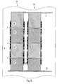
- Fig. 5 is an example (it is not a part of the invention) outlined. In the following, only the distinction to the previously illustrated embodiments will be discussed. Unless otherwise stated, the above statements also apply mutatis mutandis to this embodiment.
- the reference numerals are used analogously.
- a series connection of the OLED modules 2, 2 ', 2 "of the first column S1 or of the second column S2 or, if appropriate, further columns is provided here, as a result of which the arm 102 of the first electrical conductor 10 is no longer required and thus a distance a between the first column S1 and the second column S2 or, more generally between two adjacent columns can be reduced going on.
- This is advantageous with respect to a homogeneously appearing emission of the light emitting element.
- the individual columns S1, S2 can thereby be connected in parallel with each other.
- each of the conductor regions 81 ', 81 ", 81"' can be provided, each between the OLED modules 2, 2 ', 2 "of the first column S1 on the one hand
- the arrangement is such that, in a middle region of the first column S1, each of the conductor regions 81 ', 81 "is in each case arranged overlapping between two adjacent ones of the OLED modules and, on the one hand, with the anode of the one the two OLED modules is electrically connected and on the other hand with the cathode of the other of the two OLED modules.
- the conductor region 81 ' is electrically connected, on the one hand, to the anode of the OLED module 2' and, on the other hand, to the cathode of the first OLED module 2.
- the conductor region 81 is electrically connected on the one hand to the anode of the OLED module 2" and on the other hand to the cathode of the OLED module 2 '.
- the conductor region 81 is electrically connected to the anode of the first OLED module 2 and the conductor region 81 "'to the cathode of the OLED module 2".
- OLED modules basically represent flat luminous bodies which have a - in comparison to conventional LEDs (LED: light emitting diode) - moderate luminance, they are suitable for the production of flat diffuse light sources. Especially in the professional lighting sector, diffuse lighting is a new possibility for the realization of large-area, high-quality luminaires. In the future, the OLED can be made possible by their thin-film technology and the realization of flexible or bendable lighting bodies, which allow completely new applications in the lighting of rooms.
- the present invention shows an efficient and comparatively easy to manufacture design of a corresponding lighting element.
- the luminous element described here can be used directly as a luminaire.
- the luminous element is the only light source of the luminaire.
- a luminaire which has a luminaire housing with a light exit opening wherein a luminous element according to the invention is arranged as a light source within the luminaire housing, in such a way that a light emitted by the luminous element can leave the luminaire through the light exit area.
- a plurality of lighting elements may be provided as a corresponding light source.
Landscapes
- Physics & Mathematics (AREA)
- Optics & Photonics (AREA)
- Electroluminescent Light Sources (AREA)
Description
Die Erfindung betrifft ein Leuchtelement mit einem ersten OLED-Modul (OLED: organische lichtemittierenden Diode) und einem zweiten OLED-Modul, die auf einem Trägerelement angeordnet sind, sowie mit elektrischen Leitern zur elektrischen Stromversorgung der beiden OLED-Module. Außerdem betrifft die Erfindung eine Leuchte mit einem derartigen Leuchtelement.The invention relates to a light-emitting element having a first OLED module (OLED: organic light-emitting diode) and a second OLED module, which are arranged on a carrier element, as well as electrical conductors for the electrical power supply of the two OLED modules. Moreover, the invention relates to a luminaire with such a luminous element.
Durch eine OLED kann ein Lichtabgabeelement mit einem flächig ausgebildeten Lichtabgabebereich zur diffusen Lichtabgabe gebildet werden.An OLED can be used to form a light-emitting element with a flat light emission area for diffuse light emission.
Aus dem Stand der Technik ist eine OLED bekannt, die eine Anode als erste Elektrode in Form einer transparenten ITO-Schicht (ITO: Indium-Zinn-Oxid) aufweist, eine Kathode als zweite Elektrode in Form einer metallischen Schicht sowie eine zwischen der Anode und der Kathode angeordnete organische Schicht, die zur Lichterzeugung dient. Das von der organischen Schicht erzeugte Licht wird durch die transparente ITO-Schicht hindurch nach außen abgegeben.From the prior art, an OLED is known, which has an anode as the first electrode in the form of a transparent ITO layer (ITO: indium tin oxide), a cathode as a second electrode in the form of a metallic layer and one between the anode and the cathode arranged organic layer which serves to generate light. The light generated by the organic layer is released through the transparent ITO layer to the outside.
Die Anode weist eine Schichtstärke bzw. -dicke von ca. 100 nm auf, die Kathode eine Schichtstärke von etwa 100 bis 500 nm und die organische Schicht eine Schichtstärke von etwa 100 bis 200 nm. Die organische Schicht kann mehrere, beispielsweise sieben, Sublagen aufweisen.The anode has a layer thickness of about 100 nm, the cathode has a layer thickness of about 100 to 500 nm and the organic layer has a layer thickness of about 100 to 200 nm. The organic layer can have several, for example seven, subleaves ,
Eine OLED ist ein stromgetriebenes Bauelement, bei dem in der Regel eine möglichst homogene Stromdichteverteilung und damit verbunden eine möglichst homogen erscheinende Lichtabgabe erwünscht ist. Die ITO-Schicht weist einen vergleichsweise hochohmigen Flächenwiderstand auf; dieser kann im Bereich von 10 bis 20 Ohm/Fläche liegen. Ein Kontaktbereich zur elektrischen Kontaktierung der ITO-Schicht ist dabei lediglich am Rand der OLED möglich. Daher kommt es im Fall eines vergleichsweise großflächigen Lichtabgabebereichs zu einer Inhomogenität der Stromeinspeisung, die zu einer sichtbaren Inhomogenität der Lichtabgabe führt. Somit ist für eine entsprechende OLED mit einer Lichtabgabe, die über den gesamten Lichtabgabebereich gleichmäßig erscheint, die Flächengröße des Lichtabgabebereichs auf maximal etwa 50 mm mal 50 mm limitiert.An OLED is a current-driven component in which as homogeneous a current density distribution as possible and, associated therewith, a light output that appears as homogeneous as possible are desired. The ITO layer has a comparatively high-resistance surface resistance; this can be in the range of 10 to 20 ohms / square. A contact region for electrical contacting of the ITO layer is only possible at the edge of the OLED. Therefore, in the case of a comparatively large light output range, inhomogeneity of the power supply occurs, which leads to a visible inhomogeneity of the light output. Consequently For a corresponding OLED with a light output that appears uniform over the entire light output range, the area size of the light output range is limited to a maximum of about 50 mm by 50 mm.
Um größere abstrahlende Flächen zu realisieren, ist weiterhin bekannt, Metallverstärkungen in Form von Netzen, so genannte "Metallgrids" oder "Busbars", in die ITO-Schicht einzubringen. Hierdurch lässt sich der effektive Schichtwiderstand entsprechend der Beleuchtungsdichte erniedrigen, so dass größere gleichmäßig leuchtende Lichtabgabebereiche gebildet werden können. Allerdings bestehen diese Metallverstärkungen aus nicht lichtdurchlässigem Material, so dass die Lichtabgabe insgesamt reduziert ist. Metallgrids sind daher nur sinnvoll, wenn sie maximal ca. 25% der ITO-Fläche einnehmen. Eine mögliche Verbesserung wäre eine Erniedrigung des Widerstands durch Erhöhung der Dicke bzw. Stärke der Metallgrids; allerdings ist dies aufgrund von Strukturierungsmöglichkeiten und aufgrund der Schichtdicken der organischen Schichten nicht sinnvoll. Außerdem wird eine metallverstärkte ITO-Schicht lediglich an ihren Außenkanten elektrisch kontaktiert, so dass trotz eines verringerten Widerstands auch mit einem Metallgrid die maximale Flächengröße des Lichtabgabebereichs zur Erzielung einer homogenen Lichtabgabe limitiert ist.In order to realize larger radiating surfaces, it is also known to introduce metal reinforcements in the form of nets, so-called "metal grids" or "busbars", into the ITO layer. As a result, the effective sheet resistance can be lowered in accordance with the illumination density, so that larger uniformly luminous light emission areas can be formed. However, these metal reinforcements made of non-translucent material, so that the light output is reduced overall. Metal grids are therefore only useful if they occupy a maximum of about 25% of the ITO area. A possible improvement would be to lower the resistance by increasing the thickness of the metal grids; However, this is not meaningful due to structuring options and due to the layer thicknesses of the organic layers. In addition, a metal-reinforced ITO layer is electrically contacted only at its outer edges, so that despite a reduced resistance even with a Metallgrid the maximum area size of the light emitting area is limited to achieve a homogeneous light output.
Somit ist es erforderlich, zur Realisierung eines entsprechenden Leuchtelements mit einer, in diesem Sinne größeren Lichtabgabefläche mehrere OLEDs zu verwenden, die entsprechend zu einer größeren Fläche zusammengesetzt sind. Mit "OLED-Modul" wird vorliegend eine derartige Baueinheit bezeichnet.Thus, it is necessary to use a plurality of OLEDs, which are composed corresponding to a larger area for the realization of a corresponding light-emitting element with a, in this sense larger light output surface. With "OLED module" is referred to in the present case, such a unit.
Beispielsweise kann ein OLED-Modul einen rechteckigen bzw. quadratischen Lichtabgebebereich aufweisen, dessen Kantenlängen im Bereich von einigen Zentimetern liegen.By way of example, an OLED module can have a rectangular or square light-emitting region whose edge lengths are in the range of a few centimeters.
Aus der Schrift
Der Erfindung liegt die Aufgabe zugrunde, ein entsprechendes Leuchtelement anzugeben, das bei guten Leuchteigenschaften einfach hergestellt werden kann. Außerdem soll eine Leuchte mit einem solchen Leuchtelement angegeben werden.The invention has for its object to provide a corresponding lighting element that can be easily produced with good lighting properties. In addition, a lamp should be specified with such a light element.
Diese Aufgabe wird gemäß der Erfindung mit den in den unabhängigen Ansprüchen genannten Gegenständen gelöst. Besondere Ausführungsarten der Erfindung sind in den abhängigen Ansprüchen angegeben.This object is achieved according to the invention with the objects mentioned in the independent claims. Particular embodiments of the invention are indicated in the dependent claims.
Gemäß der Erfindung ist ein Leuchtelement vorgesehen, das ein erstes OLED-Modul und ein zweites OLED-Modul aufweist, sowie ein Trägerelement, auf dem das erste OLED-Modul und das zweite OLED-Modul angeordnet sind. Weiterhin weist das Leuchtelement elektrische Leiter zur elektrischen Stromversorgung des ersten OLED-Moduls und des zweiten OLED-Moduls auf. Dabei weist das erste OLED-Modul wenigstens drei elektrische Kontaktbereiche zur Versorgung mit elektrischem Strom auf und das zweite OLED-Modul weist wenigstens drei weitere elektrische Kontaktbereiche zur Versorgung mit elektrischem Strom auf. Jeder der Kontaktbereiche ist jeweils mit einem der Leiter elektrisch leitend verbunden. Die elektrischen Leiter sind zumindest teilweise auf dem Trägerelement angeordnet; dabei sind die Leiter derart auf dem Trägerelement angeordnet, dass sie sich nicht überkreuzen.According to the invention, a luminous element is provided, which has a first OLED module and a second OLED module, and a carrier element, on which the first OLED module and the second OLED module are arranged. Furthermore, the luminous element has electrical conductors for the electrical power supply of the first OLED module and the second OLED module. In this case, the first OLED module has at least three electrical contact regions for the supply of electrical current, and the second OLED module has at least three further electrical contact regions for the supply of electrical current. Each of the contact areas is in each case electrically conductively connected to one of the conductors. The electrical conductors are at least partially disposed on the carrier element; In this case, the conductors are arranged on the carrier element such that they do not cross over.
Durch die wenigstens drei Kontaktbereiche des ersten OLED-Moduls und die wenigstens drei weiteren Kontaktbereiche des zweiten OLED-Moduls lässt sich eine besonders homogene Stromeinspeisung in die beiden OLED-Module und somit eine besonders gleichmäßige Lichtabgabe des Leuchtmoduls erzielen; durch die besondere, kreuzungsfreie Anordnung der elektrischen Leiter auf dem Trägerelement ist dabei eine besonders einfache Herstellung des Leuchtelements ermöglicht. Außerdem lässt sich ein besonders gleichförmiges optisches Erscheinungsbild des Leuchtelements erzielen, wenn sich die Leiter auf dem Trägerelement nicht überkreuzen.Due to the at least three contact regions of the first OLED module and the at least three further contact regions of the second OLED module, a particularly homogeneous current feed into the two OLED modules and thus a particularly uniform light output of the light module can be achieved; Due to the special, crossing-free arrangement of the electrical conductors on the support element a particularly simple production of the light element is possible. In addition, a particularly uniform optical appearance of the light-emitting element can be achieved if the conductors do not cross over on the carrier element.
Eine besonders gleichförmige Stromeinspeisung in das erste OLED-Modul lässt sich erzielen, wenn das erste OLED-Modul derart geformt ist, dass es einen ersten Randbereich aufweist und einen zweiten Randbereich, der dem ersten Randbereich gegenüberliegt, wobei ein erster Kontaktbereich der drei Kontaktbereiche mit einer ersten Elektrode des ersten OLED-Moduls elektrisch verbunden ist, ein zweiter Kontaktbereich der drei Kontaktbereiche ebenfalls mit der ersten Elektrode des ersten OLED-Moduls elektrisch verbunden ist und der erste Kontaktbereich an dem ersten Randbereich angeordnet ist und der zweite Kontaktbereich an dem zweiten Randbereich. Hierdurch wird eine Stromeinspeisung (bzw. Stromableitung) von zwei gegenüberliegenden Seiten an dem ersten OLED-Modul erzielt, wodurch eine verbesserte Gleichförmigkeit der Stromdichte und somit der Lichtabgabe ermöglicht ist.A particularly uniform current feed into the first OLED module can be achieved if the first OLED module is shaped such that it has a first edge region and a second edge region, which lies opposite the first edge region, wherein a first contact region of the three contact regions the first electrode of the first OLED module is electrically connected, a second contact region of the three contact regions is also electrically connected to the first electrode of the first OLED module and the first contact region on the first Edge region is arranged and the second contact region at the second edge region. As a result, a power supply (or current dissipation) is achieved from two opposite sides of the first OLED module, whereby an improved uniformity of the current density and thus the light output is enabled.
Vorzugsweise weist dabei das erste OLED-Modul eine rechteckige Form, insbesondere eine quadratische Form auf, wobei der erste Randbereich durch einen ersten Seitenbereich der vier, durch die Form festgelegten Seitenbereiche gegeben ist und der zweite Randbereich durch denjenigen weiteren Seitenbereich, der dem ersten Seitenbereich gegenüberliegt oder der erste Randbereich durch einen, durch die Form festgelegten, ersten Eckenbereich gegeben ist und der zweite Randbereich durch einen weiteren Eckenbereich, der dem ersten Eckenbereich gegenüberliegt.In this case, the first OLED module preferably has a rectangular shape, in particular a square shape, wherein the first edge region is given by a first side region of the four side regions defined by the shape, and the second edge region by that further side region which is opposite to the first side region or the first edge region is given by a first corner region defined by the shape, and the second edge region by a further corner region, which is opposite to the first corner region.
Eine insgesamt besonders großflächig erscheinende Lichtabgabefläche des Leuchtelements lässt sich vorteilhaft erzielen, wenn - wie erfindungsgemäß vorgesehen - das Leuchtelement außerdem mehrere weitere OLED-Module aufweist, die ebenfalls auf dem Trägerelement angeordnet sind, wobei das erste OLED-Modul, das zweite OLED-Modul und die weiteren OLED-Module derart auf dem Trägerelement angeordnet sind, dass sie Reihen und Spalten bilden. Dabei ist auf dem Trägerelement in einem Grenzbereich zwischen zwei der Spalten ein Arm eines ersten elektrischen Leiters der elektrischen Leiter angeordnet.A light emitting area of the luminous element that appears to be particularly large overall can be advantageously achieved if, as provided for by the invention, the luminous element also has a plurality of further OLED modules which are likewise arranged on the carrier element, the first OLED module, the second OLED module and the further OLED modules are arranged on the carrier element in such a way that they form rows and columns. In this case, an arm of a first electrical conductor of the electrical conductors is arranged on the carrier element in a boundary region between two of the columns.
Erfindungsgemäß sind dabei diejenigen der OLED-Module, die eine der zwei Spalten bilden, elektrisch parallel geschaltet und mit dem Arm des ersten elektrischen Leiters elektrisch verbunden. Vorzugsweise ist dabei außerdem ein Arm eines zweiten elektrischen Leiters der elektrischen Leiter derart auf dem Trägerelement angeordnet, dass er sich zwischen denjenigen OLED-Modulen, die die eine der zwei Spalten bilden, einerseits und dem Trägerelement andererseits erstreckt. Auf diese Weise ist eine besonders einfache, kreuzungsfreie Anordnung der Leiter auf dem Trägerelement, insbesondere für eine Parallelschaltung der OLED-Module der betreffenden Spalte, ermöglicht.According to the invention, those of the OLED modules that form one of the two columns are electrically connected in parallel and electrically connected to the arm of the first electrical conductor. In this case, moreover, an arm of a second electrical conductor of the electrical conductors is arranged on the carrier element such that it extends between those OLED modules which form one of the two columns, on the one hand, and the carrier element on the other hand. In this way, a particularly simple, crossing-free arrangement of the conductors on the carrier element, in particular for a parallel connection of the OLED modules of the relevant column, allows.
Eine besonders große Lichtabgabefläche des Leuchtelements lässt sich vorteilhaft erzielen, wenn das erste OLED-Modul, das zweite OLED-Modul und die weiteren OLED-Module jeweils eine Lichtabgabefläche aufweisen, die größer ist als 1 cm2, vorzugsweise größer als 4 cm2, besonders bevorzugt größer als 20 cm2 A particularly large light emission area of the luminous element can be advantageously achieved if the first OLED module, the second OLED module and the further OLED modules each have a light emission area that is greater than 1 cm 2 , preferably greater than 4 cm 2 , especially preferably greater than 20 cm 2
Vorteilhaft weist ein elektrischer Leiter der elektrischen Leiter einen zumindest teilweise lichtdurchlässigen Leiterbereich auf, der zwischen dem ersten OLED-Modul und dem Trägerelement angeordnet ist. Hierdurch ist eine im Wesentlichen ungehinderte Lichtabgabe des OLED-Moduls in zwei entgegengesetzte Richtungen ermöglicht. Insbesondere lässt sich durch diese Ausgestaltung erzielen, dass der Leiterbereich die Lichtabgabe des Leuchtelements nicht nennenswert beeinträchtigt, beispielsweise durch Streuung an Randbereichen bzw. Kanten des Leiters oder dergleichen. Besonders vorteilhaft lässt sich dies erzielen, wenn das Leuchtelement derart gestaltet ist, dass, in einem Querschnitt durch den ersten Kontaktbereich und den zweiten Kontaktbereich und das Trägerelement betrachtet, zwischen dem ersten OLED-Modul und dem Trägerelement ein länglicher Zwischenraum gebildet ist und der Leiterbereich mehr als die Hälfte, vorzugsweise mehr als 80%, besonders bevorzugt 100% der Längserstreckung des Zwischenraums einnimmt. Auf diese Weise lassen sich insbesondere Kanten des Leiters, die eine Lichtabgabe negativ beeinflussen könnten, zuverlässig verhindern.Advantageously, an electrical conductor of the electrical conductors has an at least partially translucent conductor region, which is arranged between the first OLED module and the carrier element. As a result, a substantially unimpeded light output of the OLED module in two opposite directions is possible. In particular, it can be achieved by this refinement that the conductor region does not appreciably impair the light output of the luminous element, for example due to scattering at edge regions or edges of the conductor or the like. This can be achieved particularly advantageously if the luminous element is designed in such a way that, viewed in a cross section through the first contact region and the second contact region and the carrier element, an elongated intermediate space is formed between the first OLED module and the carrier element and the conductor region is longer than half, preferably more than 80%, particularly preferably 100% of the longitudinal extent of the intermediate space occupies. In this way, in particular edges of the conductor, which could adversely affect a light output, reliably prevent.
Vorzugsweise sind dabei die OLED-Module derjenigen Spalte, in der sich das erste OLED-Modul befindet, elektrisch in Reihe oder parallel geschaltet sind. Die weiteren Spalten können analog elektrisch geschaltet sein.Preferably, the OLED modules of that column in which the first OLED module is located are electrically connected in series or in parallel. The other columns can be electrically connected in the same way.
Vorteilhaft ist das Trägerelement zumindest teilweise lichtdurchlässig und besteht dabei beispielsweise aus Glas, PMMA (Polymethylmethacrylat) oder aus einer Folie, beispielsweise aus PET (Polyethylenterephthalat) oder es ist nicht lichtdurchlässig und besteht dabei beispielsweise aus Metall oder Kunststoff.Advantageously, the carrier element is at least partially translucent and consists for example of glass, PMMA (polymethylmethacrylate) or of a film, for example of PET (polyethylene terephthalate) or it is not translucent and consists for example of metal or plastic.
Die drei elektrischen Kontaktbereiche sind vorzugsweise jeweils mit einem der Leiter über einen Leitkleber, eine Weichlötung, ein Flexkabel, einen Klemmkontakt oder einen mechanischen Federkontakt elektrisch leitend verbunden.The three electrical contact areas are preferably each electrically connected to one of the conductors via a conductive adhesive, a soft solder, a flex cable, a terminal contact or a mechanical spring contact.
Die elektrischen Leiter sind vorteilhaft aus einem Metall, wie beispielsweise Aluminium, Silber, Chrom oder Kupfer oder aus einer Metalllegierung gebildet, das bzw. die auf dem Trägerelement aufgebracht ist. Die elektrischen Leiter können vorteilhaft auch aus einem transparenten Material gebildet sein, beispielsweise aus ITO oder FTO (Fluor dotiertes Zinnoxid) oder ZnO (Zink Oxid) oder PEDOT (Poly-3,4-ethylendioxythiophen), das auf dem Trägerelement aufgebracht ist.The electrical conductors are advantageously formed from a metal, such as aluminum, silver, chromium or copper or a metal alloy, which is or is applied to the carrier element. The electrical conductors can advantageously also be formed of a transparent material, for example of ITO or FTO (fluorine-doped tin oxide) or ZnO (zinc oxide) or PEDOT (poly-3,4-ethylenedioxythiophene), which is applied to the carrier element.
Gemäß einem weiteren Aspekt der Erfindung ist eine Leuchte, insbesondere zur Raumbeleuchtung, vorgesehen, die ein erfindungsgemäßes Leuchtelement aufweist. Dabei kann das Leuchtelement vorteilhaft die einzige Lichtquelle der Leuchte darstellen.According to a further aspect of the invention, a luminaire, in particular for room lighting, is provided which has a luminous element according to the invention. In this case, the lighting element can advantageously represent the only light source of the lamp.
Die Erfindung wird im Folgenden anhand von Ausführungsbeispielen und mit Bezug auf die Zeichnungen näher erläutert. Es zeigen:
- Fig. 1
- eine Skizze zu einem ersten Ausführungsbeispiel eines erfindungsgemäßen Leuchtelements,
- Fig. 2
- eine Skizze zu einer Variante des in
Fig. 1 gezeigten Leuchtelements, - Fig. 3
- eine Querschnitt-Skizze zu der in
Fig. 2 gezeigten Variante, - Fig. 4
- eine Skizze zu einem zweiten Ausführungsbeispiel,
- Fig. 4a
- eine Querschnitt-Skizze zu dem in
Fig. 4 gezeigten Ausführungsbeispiel und - Fig. 5
- eine Skizze zu einem Beispiel. (Es handelt sich dabei nicht um einen Teil der Erfindung.)
- Fig. 1
- a sketch of a first embodiment of a luminous element according to the invention,
- Fig. 2
- a sketch to a variant of in
Fig. 1 shown luminous element, - Fig. 3
- a cross-sectional sketch of the in
Fig. 2 shown variant, - Fig. 4
- a sketch of a second embodiment,
- Fig. 4a
- a cross-sectional sketch of the in
Fig. 4 shown embodiment and - Fig. 5
- a sketch for an example. (It is not a part of the invention.)
In
Insbesondere kann das erste OLED-Modul 2 weiterhin derart gestaltet sein, dass sich die genannten drei Schichten jeweils bis an seitliche Randbereiche des OLED-Moduls 2 erstrecken. Außerdem kann das erste OLED-Modul 2 biegsam bzw. flexibel sein. Das zweite OLED-Modul 4 kann in entsprechender Weise aufgebaut sein.In particular, the
Weiterhin weist das Leuchtelement ein Trägerelement 6 auf, auf dem das erste OLED-Modul 2 und das zweite OLED-Modul 4 angeordnet sind. Bei dem Trägerelement 6 kann es sich um ein im Wesentlichen zweidimensionales Bauteil handeln, also beispielsweise um ein plattenförmiges Bauteil, so dass zwei gegenüberliegende, große Flachseiten gebildet sind, wobei die beiden OLED-Module 2, 4 vorzugsweise auf lediglich einer der beiden Flachseiten angeordnet sind. Das Trägerelement 6 kann dabei biegsam bzw. flexibel sein. Insbesondere können die beiden OLED-Module 2, 4 auf dem Trägerelement 6 jeweils mechanisch fixiert sein, vorzugsweise unmittelbar mechanisch fixiert sein, beispielsweise über eine Verschraubung und/oder eine Verklebung.Furthermore, the luminous element has a
Außerdem weist das Leuchtelement elektrische Leiter 8, 10 auf, die einer elektrischen Stromversorgung der beiden OLED-Module 2, 4 dienen, und zwar umfassend einen ersten Leiter 10 und einen zweiten Leiter 8.In addition, the luminous element has
Das erste OLED-Modul 2 weist drei Kontaktbereiche 22, 24, 26 zur Versorgung mit elektrischem Strom auf, und zwar einen ersten Kontaktbereich 22, einen zweiten Kontaktbereich 24 und einen dritten Kontaktbereich 26. Die drei Kontaktbereiche 22, 24, 26 können - wie in
Das zweite OLED-Modul 4 weist drei weitere Kontaktbereiche 42, 44, 46 zur Versorgung mit elektrischem Strom auf, die vorzugsweise in analoger Weise zu den zuerst genannten drei Kontaktbereichen 22, 24, 26 ausgebildet sind.The
Jeder der Kontaktbereiche 22, 24, 26, 42, 44, 46 ist mit einem der beiden elektrischen Leiter 8, 10 elektrisch leitend verbunden. Im gezeigten Beispiel ist der erste Kontaktbereich 22 mit dem zweiten Leiter 8 verbunden, der zweite Kontaktbereich 24 ebenfalls mit dem zweiten Leiter 8 und der dritte Kontaktbereich 26 mit dem ersten Leiter 10. Beispielsweise können in diesem Fall der erste Kontaktbereich 22 und der zweite Kontaktbereich 24 mit der Anode des ersten OLED-Moduls 2 elektrisch leitend verbunden sein und der dritte Kontaktbereich 26 mit der Kathode des ersten OLED-Moduls 2. Dies ist insbesondere vorteilhaft, wenn die Anode einen vergleichsweise hohen Widerstand aufweist, wie das beispielsweise der Fall ist, wenn die Anode aus einer ITO-Schicht gebildet ist.Each of the
In analoger Weise sind im gezeigten Beispiel die weiteren Kontaktbereiche 42 und 44 des zweiten OLED-Moduls 4 mit dem zweiten Leiter 8 verbunden und der weitere Kontaktbereich 46 mit dem ersten Leiter 10.In an analogous manner, the
Es sei jedoch ausdrücklich erwähnt, dass auch zwei der drei Kontaktbereiche 22, 24, 26 des ersten OLED-Moduls 2 mit der Kathode des ersten OLED-Moduls 2 verbunden sein können und der entsprechend dritte Kontaktbereich mit der Anode. Entsprechendes gilt für das zweite OLED-Modul 4.However, it is expressly mentioned that two of the three
Die Verbindung zwischen dem ersten Kontaktbereich 22 und dem zweiten Leiter 8 kann beispielsweise über einen Leitkleber, eine Weichlötung, ein Flexkabel, einen Klemmkontakt oder einen mechanischen Federkontakt vorgesehen sein. Entsprechendes gilt auch für die jeweiligen Verbindungen zwischen dem zweiten Kontaktbereich 24, dem dritten Kontaktbereich 26 bzw. den weiteren drei Kontaktbereichen 42, 44, 46 und jeweils dem betreffenden der elektrischen Leiter 8, 10.The connection between the
Die elektrischen Leiter 8, 10 sind zumindest teilweise auf dem Trägerelement 6 angeordnet bzw. aufgebracht. Dabei sind die Leiter 8, 10 derart auf dem Trägerelement 6 angeordnet, dass sie sich nicht überkreuzen. Hierdurch ist eine besonders einfache Herstellung des Leuchtelements ermöglicht. Außerdem ist hierdurch ermöglicht, dass das Erscheinungsbild des Leuchtelements keine Kreuzungspunkte von elektrischen Leitern aufweist und daher besonders ebenmäßig ist. Dies ist insbesondere von Vorteil, wenn das Leuchtelement als Lichtquelle einer Leuchte, beispielsweise zur Raumbeleuchtung verwendet wird.The
Die elektrischen Leiter 8, 10 können aus einem Metall gebildet sein, wie beispielsweise Aluminium, Silber, Chrom oder Kupfer. Sie können auch aus einer Metalllegierung gebildet sein. Sie können auch aus einem transparenten Material gebildet sein, beispielsweise aus ITO oder FTO oder ZnO oder PEDOT. Dabei kann das betreffende Material auf dem Trägerelement 6 - vorzugsweise unmittelbar auf einer Oberfläche des Trägerelements 6 - aufgebracht sein. Insbesondere können die Leiter 8, 10 auf lediglich einer der beiden Flachseiten des Trägerelements 6 angeordnet sein, insbesondere auf derselben Flachseite wie die beiden OLED-Module 2, 4.The
Die Anordnung der elektrischen Leiter 8, 10 unmittelbar auf dem Trägerelement 6 kann derart gestaltet sein, dass die Abstände zwischen den Kontaktbereichen 22, 24, 26 usw. einerseits und den Leitern 8, 10 bzw. Armen der Leiter 8, 10 unmittelbar auf dem Trägerelement 6 andererseits weniger als 5 mm, vorzugsweise weniger als 2 mm betragen.The arrangement of the
Wie in
Wenn, wie in
Für die weiteren drei Kontaktbereiche 42, 44, 46 des zweiten OLED-Moduls 4 gilt Analoges.For the other three
Wie in
Lediglich beispielhaft ist in
Beispielsweise kann jedes der OLED-Module 2, 2', 2", 4, 4', 4" einen Lichtabgabebereich mit einer Fläche aufweisen, die größer als 1 cm2 ist, vorzugsweise größer als 4 cm2, besonders bevorzugt größer als 20 cm2. Es können OLED-Module verwendet werden, deren Lichtabgabebereiche jeweils eine Fläche von mehr als 25 cm2 aufweisen. Insbesondere können sämtliche OLED-Module 2, 2', 2", 4, 4', 4" des Leuchtelements Lichtabgabebereiche mit ein und derselben Flächengröße aufweisen.For example, each of the
Die Abstände zwischen den OLED-Modulen 2, 2', 2", 4, 4', 4" können im Vergleich zu der Größe der Lichtabgabereiche verhältnismäßig klein sein, so dass alle OLED-Module 2, 2', 2", 4, 4', 4" zusammen insgesamt den Eindruck lediglich einer, entsprechend großen, zusammengehörigen Lichtabgabefläche des Leuchtelements erwecken. Beispielsweise kann vorgesehen sein, dass die Abstände zwischen den OLED-Modulen 2, 2', 2", 4, 4', 4" weniger als 1 cm, beispielsweise zwischen 1 mm und 1cm betragen. Es kann auch vorgesehen sein, dass die Abstände im Fall von rechteckigen OLED-Modulen weniger als 30%, vorzugsweise weniger als 15% oder weniger als 10% einer der Kanten- bzw. Seitenlängen eines der OLED-Module 2, 2', 2", 4, 4', 4" betragen.The distances between the
Eine einfache kreuzungsfreie Anordnung der Leiter 8, 10 auf dem Trägerelement 6 ist in diesem Fall ermöglicht, wenn auf dem Trägerelement 6 in einem Grenzbereich zwischen zwei der Spalten S1, S2 ein Arm 102 eines der elektrischen Leiter, im gezeigten Beispiel des ersten elektrischen Leiters 10, angeordnet ist.A simple, crossing-free arrangement of the
Diese Anordnung ist besonders vorteilhaft, wenn diejenigen der OLED-Module 2, 2', 2", 4, 4', 4", die eine der zwei Spalten S1, S2 bilden, elektrisch parallel geschaltet sind und mit dem Arm 102 verbunden sind. Hierzu kann der Arm 102 auf dem Trägerelement 6 insbesondere so angeordnet sein, dass er sich zur elektrischen Verbindung mit allen OLED-Modulen 2, 2', 2" der betreffenden Spalte S1 eignet. In dem in
Wie ebenfalls in
In
Entsprechend kann auch ein weiterer Arm 84 des weiteren bzw. des zweiten Leiters 8 zur Realisierung der beschriebenen gegenüberliegenden Stromeinspeisung auf dem Trägerelement 6 vorgesehen sein, der insbesondere mit Bezug auf die betreffende Spalte S1 gegenüberliegend von dem zuerst genannten Arm 82 des weiteren bzw. des zweiten Leiters 8 angeordnet ist.Accordingly, a
Natürlich kann im Fall von mehreren Spalten die oben beschriebene Anordnung für jede der Spalten in analoger Weise vorgesehen sein.Of course, in the case of multiple columns, the arrangement described above may be provided for each of the columns in an analogous manner.
In
Eine Lichtabgabe des Leuchtelements kann in eine erste Richtung o vorgesehen sein, mit Bezug auf
Der Arm 82 des zweiten Leiters 8 kann so gestaltet sein, dass er sich lediglich entlang von Randbereichen 50, 50', 50" der betreffenden OLED-Module 2, 2', 2" erstreckt. Auf diese Weise lässt sich erzielen, dass eine Lichtabgabe der betreffenden OLED-Module 2, 2', 2" durch den Arm 82 besonders wenig beeinträchtigt ist. Beispielsweise kann vorgesehen sein, dass die betreffenden Randbereiche 50, 50', 50" lediglich eine Breite x1 aufweisen, die kleiner ist als 25%, vorzugsweise kleiner als 20% oder kleiner als 10% einer Kantenlänge B der OLED-Module 2, 2', 2", beispielsweise der Breite der betreffenden Spalte S1. Entsprechendes gilt für den weiteren Arm 84 des zweiten Leiters 8; die den zuletzt genannten Arm 84 in diesem Sinne betreffenden Randbereiche können dementsprechend eine Breite x2 aufweisen, die kleiner ist als 25%, vorzugsweise kleiner als 20% oder kleiner als 10% der Kantenlänge B. Auf diese Weise ist ermöglicht, dass die OLED-Module 2, 2', 2" der betreffenden Spalte S1 über eine Breite x2 = B - x1 - x2 in ihrer Lichtabgabe in die zweite Richtung u bzw. nach unten im Wesentlichen durch keinen elektrischen Leiter bzw. Arm eines elektrischen Leiters beeinträchtigt sind.The
In
Im Unterschied zum ersten Ausführungsbeispiel weist einer der Leiter 8, 10, hier beispielhaft der zweite Leiter 8, einen Leiterbereich 80 auf, der zwischen dem ersten OLED-Modul 2 und dem Trägerelement 6 angeordnet ist und dabei zumindest teilweise lichtdurchlässig gestaltet ist. Hierzu kann der Leiterbereich 80 aus einem transparenten Material gebildet sein, beispielsweise aus ITO oder FTO oder ZnO oder PEDOT. Auch die weiteren Bereiche des zweiten Leiters 8 bzw. weitere Leiter 10 können entsprechend ausgebildet und angeordnet sein.In contrast to the first exemplary embodiment, one of the
In
Auf diese Weise kann der Leiterbereich 80 so großflächig ausgestaltet sein, dass er keine Ränder bzw. Kanten bildet, die die Lichtabgabe in die zweite Richtung u bzw. nach "unten" nennenswert stören könnten.In this way, the
Wie wiederum aus
Für die weiteren OLED-Module 2', 2" der betreffenden Spalte S1 gilt entsprechendes, so dass weitere entsprechende Leiterbereiche 80', 80" gebildet sind. Ebenso gilt entsprechendes für die zweite Spalte S2 bzw. gegebenenfalls für weitere Spalten.For the
In den anhand der
In dem in
In dem in
Natürlich ist eine entsprechende Modifizierung der Widerstände auch in den anderen Ausführungsbeispielen möglich.Of course, a corresponding modification of the resistors is also possible in the other embodiments.
In
Im Unterschied zu den bisherigen Ausführungsbeispielen ist hier eine Reihenschaltung der OLED-Module 2, 2', 2" der ersten Spalte S1 bzw. der zweiten Spalte S2 bzw. gegebenenfalls weiterer Spalten vorgesehen. Hierdurch ist der Arm 102 des ersten elektrischen Leiters 10 nicht mehr erforderlich und somit lässt sich ein Abstand a zwischen der ersten Spalte S1 und der zweiten Spalte S2 bzw. allgemeiner zwischen zwei benachbarten Spalten weitergehend verringern. Dies ist vorteilhaft mit Bezug auf eine möglichst homogen erscheinende Abstrahlung des Leuchtelements. Die einzelnen Spalten S1, S2 können dabei untereinander parallel geschaltet sein.In contrast to the previous exemplary embodiments, a series connection of the
Zur Realisierung der Reihenschaltung innerhalb der Spalte S1 können insbesondere mehrere, im gezeigten Beispiel vier Leiterbereiche 81, 81', 81 ", 81"' vorgesehen sein, die jeweils zwischen den OLED-Module 2, 2', 2" der ersten Spalte S1 einerseits und dem Trägerelement 6 andererseits angeordnet sind. Dabei ist die Anordnung derart, dass in einem mittleren Bereich der ersten Spalte S1 jeder der Leiterbereiche 81', 81" jeweils überlappend zwischen zwei benachbarten der OLED-Module angeordnet ist und dabei einerseits mit der Anode des einen der beiden OLED-Module elektrisch verbunden ist und andererseits mit der Kathode des anderen der beiden OLED-Module.To realize the series connection within the column S1 , in particular a plurality of, in the example shown, four
Im gezeigten Beispiel ist der Leiterbereich 81' einerseits mit der Anode des OLED-Moduls 2' und andererseits mit der Kathode des ersten OLED-Moduls 2 elektrisch verbunden. Der Leiterbereich 81 " einerseits mit der Anode des OLED-Moduls 2" und andererseits mit der Kathode des OLED-Moduls 2' elektrisch verbunden.In the example shown, the conductor region 81 'is electrically connected, on the one hand, to the anode of the OLED module 2' and, on the other hand, to the cathode of the
Die beiden randständigen Leiterbereiche 81, 81"' sind jeweils lediglich mit einem OLED-Modul, also mit dem ersten OLED-Modul 2 bzw. dem letzten OLED-Modul 2" der betreffenden Spalte S1 elektrisch verbunden. Im gezeigten Beispiel ist der Leiterbereich 81 mit der Anode des ersten OLED-Moduls 2 elektrisch verbunden und der Leiterbereich 81"' mit der Kathode des OLED-Moduls 2".The two
Entsprechendes gilt natürlich wiederum für die zweite Spalte S2 bzw. gegebenenfalls jeweils für weitere Spalten.Of course, the same applies in turn to the second column S2 or, if appropriate, in each case for further columns.
Da OLED-Module grundsätzlich flächige Leuchtkörper darstellen, die eine - im Vergleich zu konventionellen LEDs (LED: lichtemittierende Diode) - moderate Leuchtdichte aufweisen, eignen sie sich zur Herstellung flächiger diffuser Lichtquellen. Insbesondere im professionellen Beleuchtungsbereich ist eine diffuse Beleuchtung eine neue Möglichkeit der Realisierung von großflächigen, hochqualitativen Leuchten. Dabei kann in weiterer Zukunft die OLED durch ihre Dünnschichttechnologie auch die Realisierung von flexiblen bzw. biegbaren Leuchtkörpern ermöglicht werden, die ganz neue Anwendungen in der Beleuchtung von Räumen gestatten. Die vorliegende Erfindung zeigt eine effiziente und dabei vergleichsweise einfach herzustellende Gestaltung eines entsprechenden Leuchtelements.Since OLED modules basically represent flat luminous bodies which have a - in comparison to conventional LEDs (LED: light emitting diode) - moderate luminance, they are suitable for the production of flat diffuse light sources. Especially in the professional lighting sector, diffuse lighting is a new possibility for the realization of large-area, high-quality luminaires. In the future, the OLED can be made possible by their thin-film technology and the realization of flexible or bendable lighting bodies, which allow completely new applications in the lighting of rooms. The present invention shows an efficient and comparatively easy to manufacture design of a corresponding lighting element.
Beispielsweise kann das hier beschriebene Leuchtelement unmittelbar als Leuchte verwendet werden. In diesem Fall stellt das Leuchtelement die einzige Lichtquelle der Leuchte dar. Es können aber auch mehrere Leuchtelemente als eine Leuchte verwendet werden. Es ist auch möglich, eine Leuchte vorzusehen, die ein Leuchtengehäuse mit einer Lichtaustrittsöffnung aufweist, wobei ein erfindungsgemäßes Leuchtelement als Lichtquelle innerhalb des Leuchtengehäuses angeordnet ist, und zwar derart, dass ein von dem Leuchtelement abgegebenes Licht durch den Lichtaustrittsbereich hindurch die Leuchte verlassen kann. Natürlich können auch mehrere Leuchtelemente als entsprechende Lichtquelle vorgesehen sein.For example, the luminous element described here can be used directly as a luminaire. In this case, the luminous element is the only light source of the luminaire. However, it is also possible to use a plurality of luminous elements as one luminaire. It is also possible to provide a luminaire which has a luminaire housing with a light exit opening, wherein a luminous element according to the invention is arranged as a light source within the luminaire housing, in such a way that a light emitted by the luminous element can leave the luminaire through the light exit area. Of course, a plurality of lighting elements may be provided as a corresponding light source.
Claims (13)
- A lighting element, having- a first OLED module (2),- a second OLED module (4),- a carrier element (6) on which the first OLED module (2) and the second OLED module (4) are arranged, and- electrical conductors (8, 10) for supplying electric current to the first OLED module (2) and the second OLED module (4),
wherein the first OLED module (2) has at least three electrical contact regions (22, 24, 26) for the supply of electric current,
the second OLED module (4) has at least three further electrical contact regions (42, 44, 46) for the supply of electric current,
wherein each of the contact regions (22, 24, 26, 42, 44, 46) is connected in an electrically conductive manner to, in each case, one of the conductors (8, 10), wherein the electrical conductors (8, 10) are arranged at least in part on the carrier element (6), and wherein the conductors (8, 10) are arranged on the carrier element (6) in such a way that they do not intersect,
having, furthermore,- a plurality of further OLED modules (2', 2" , 4', 4") which are likewise arranged on the carrier element (6),
wherein the first OLED module (2), the second OLED module (4) and the further OLED modules (2', 2", 4', 4") are arranged on the carrier element (6) in such a way that they form rows (R1, R2, R3) and columns (S1, S2),
characterised in that
arranged on the carrier element (6) in a boundary region between two of the columns (S1, S2) there is an arm (102) of a first electrical conductor (10) of the electrical conductors (8, 10), wherein those modules of the OLED modules (2, 2', 2" , 4, 4', 4'') forming one of the two columns (S1, S2) are connected electrically in parallel and are connected electrically to the arm (102) of the first electrical conductor (10). - A lighting element according to claim 1,
in which the first OLED module (2) is shaped in such a way that it has a first edge region (50) and a second edge region (52) lying opposite the first edge region (50),
wherein a first contact region (22) of the three contact regions (22, 24, 26) is electrically connected to a first electrode of the first OLED module (2),
a second contact region (24) of the three contact regions (22, 24, 26) is likewise electrically connected to the first electrode of the first OLED module (2), and
wherein the first contact region (22) is arranged at the first edge region (50), and the second contact region (24) at the second edge region (52). - A lighting element according to claim 2,
in which the first OLED module (2) has a rectangular shape, in particular a square shape,
wherein the first edge region (50) is given by a first side region of the four side regions defined by the shape, and the second edge region (52) is given by that further side region lying opposite the first side region, or
the first edge region (50) is given by a first corner region defined by the shape, and the second edge region (52) is given by a further corner region lying opposite the first corner region. - A lighting element according to one of the preceding claims,
wherein, moreover, an arm (82) of a second electrical conductor (8) of the electrical conductors (8, 10) is arranged on the carrier element (6) in such a way that it extends between those OLED modules (2, 2', 2") that form the one column of the two columns (S1), on the one hand, and the carrier element (6), on the other hand. - A lighting element according to one of the preceding claims,
in which the first OLED module (2), the second OLED module (4) and the further OLED modules (2', 2", 4', 4") each have a light-emitting face that is larger than 1 cm2, preferably larger than 4 cm2, particularly preferably larger than 20 cm2. - A lighting element according to one of the preceding claims,
in which one electrical conductor (8) of the electrical conductors (8, 10) has a conductor region (80, 81) that is permeable to light at least in part and is arranged between the first OLED module (2) and the carrier element (6). - A lighting element having the features mentioned in claims 2 and 6 that is configured in such a way that, viewed in a cross section through the first contact region (22) and the second contact region (24) and the carrier element (6), an elongate interspace (90) is formed between the first OLED module (2) and the carrier element (6), and the conductor region (80, 81) occupies more than half, preferably more than 80%, particularly preferably 100%, of the longitudinal extent of the interspace (90).
- A lighting element having the features mentioned in claims 2 and 6 or a lighting element according to claim 7,
wherein the OLED modules (2, 2', 2") of that column (S1) in which the first OLED module (2) is located are connected electrically in series or parallel. - A lighting element according to one of the preceding claims,
in which the carrier element (6) is permeable to light at least in part, and consists, for example, of glass, PMMA or of a film, for example of PET, or is not permeable to light and consists, for example, of metal or plastics. - A lighting element according to one of the preceding claims,
in which the three electrical contact regions (22, 24, 26) are connected in an electrically conductive manner to, in each case, one of the conductors (8, 10) by way of a conductive adhesive, soft-soldering, a flexible cable, a clamping contact or a mechanical spring contact. - A lighting element according to one of the preceding claims,
in which the electrical conductors (8, 10) are formed from a metal, such as, for example, aluminium, silver, chromium or copper, or a metal alloy applied to the carrier element (6), or are formed from a transparent material, for example from ITO, FTO, ZnO or PEDOT, applied to the carrier element (6). - A luminaire, in particular for illuminating a room, having a lighting element according to one of the preceding claims.
- A luminaire according to claim 12,
in which the lighting element represents the sole light source of the luminaire.
Applications Claiming Priority (2)
| Application Number | Priority Date | Filing Date | Title |
|---|---|---|---|
| DE102010042132A DE102010042132A1 (en) | 2010-10-07 | 2010-10-07 | Light element with OLED modules |
| PCT/EP2011/067543 WO2012045857A1 (en) | 2010-10-07 | 2011-10-07 | Lighting element having oled modules |
Publications (3)
| Publication Number | Publication Date |
|---|---|
| EP2625731A1 EP2625731A1 (en) | 2013-08-14 |
| EP2625731B1 true EP2625731B1 (en) | 2014-07-16 |
| EP2625731B2 EP2625731B2 (en) | 2022-03-16 |
Family
ID=44759708
Family Applications (1)
| Application Number | Title | Priority Date | Filing Date |
|---|---|---|---|
| EP11764774.3A Not-in-force EP2625731B2 (en) | 2010-10-07 | 2011-10-07 | Lighting element having oled modules |
Country Status (3)
| Country | Link |
|---|---|
| EP (1) | EP2625731B2 (en) |
| DE (1) | DE102010042132A1 (en) |
| WO (1) | WO2012045857A1 (en) |
Families Citing this family (11)
| Publication number | Priority date | Publication date | Assignee | Title |
|---|---|---|---|---|
| US8552440B2 (en) | 2010-12-24 | 2013-10-08 | Semiconductor Energy Laboratory Co., Ltd. | Lighting device |
| WO2014030089A1 (en) * | 2012-08-23 | 2014-02-27 | Koninklijke Philips N.V. | Stabilized wavelength converting element |
| DE102012221095B4 (en) | 2012-11-19 | 2020-04-16 | Osram Oled Gmbh | Optoelectronic component |
| DE102012223162B4 (en) * | 2012-12-14 | 2022-08-25 | Pictiva Displays International Limited | AREA LIGHT SYSTEM |
| DE102013109822A1 (en) * | 2013-09-09 | 2015-03-12 | Osram Opto Semiconductors Gmbh | A radiation emitting device and method of making the same |
| DE102013113001B4 (en) * | 2013-09-13 | 2018-05-24 | Osram Oled Gmbh | Module and arrangement with a module |
| DE102014103751A1 (en) * | 2014-03-19 | 2015-09-24 | Osram Opto Semiconductors Gmbh | Organic radiation-emitting component |
| DE102014205747A1 (en) * | 2014-03-27 | 2015-10-01 | Tridonic Gmbh & Co Kg | Light module and manufacturing method for a light module |
| DE102014112879B4 (en) * | 2014-09-08 | 2025-02-06 | Pictiva Displays International Limited | Radiation-emitting device and method for producing the same |
| DE102015100099B4 (en) | 2015-01-07 | 2017-10-19 | Osram Oled Gmbh | Method for producing an organic light-emitting component |
| WO2018139426A1 (en) * | 2017-01-30 | 2018-08-02 | パイオニア株式会社 | Light emitting device |
Family Cites Families (9)
| Publication number | Priority date | Publication date | Assignee | Title |
|---|---|---|---|---|
| US7135728B2 (en) † | 2002-09-30 | 2006-11-14 | Nanosys, Inc. | Large-area nanoenabled macroelectronic substrates and uses therefor |
| US7108392B2 (en) † | 2004-05-04 | 2006-09-19 | Eastman Kodak Company | Tiled flat panel lighting system |
| KR101381906B1 (en) * | 2004-09-13 | 2014-04-04 | 가부시키가이샤 한도오따이 에네루기 켄큐쇼 | Lighting Device |
| FR2892594B1 (en) † | 2005-10-21 | 2007-12-07 | Saint Gobain | LIGHT STRUCTURE COMPRISING AT LEAST ONE ELECTROLUMINESCENT DIODE, ITS MANUFACTURE AND ITS APPLICATIONS |
| RU2414018C2 (en) * | 2005-12-19 | 2011-03-10 | Конинклейке Филипс Электроникс Н.В. | Organic electroluminescent device |
| DE102006016373A1 (en) * | 2006-04-05 | 2007-10-11 | Merck Patent Gmbh | Large area OLEDs with homogeneous light emission |
| US8179036B2 (en) * | 2007-01-22 | 2012-05-15 | Koninklijke Philips Electronics N.V. | Light emitting device with a shunt |
| DE602007003193D1 (en) † | 2007-04-27 | 2009-12-24 | Mechatronic System Company S R | Switch for product supply lines |
| US8022626B2 (en) † | 2008-09-16 | 2011-09-20 | Osram Sylvania Inc. | Lighting module |
-
2010
- 2010-10-07 DE DE102010042132A patent/DE102010042132A1/en not_active Withdrawn
-
2011
- 2011-10-07 EP EP11764774.3A patent/EP2625731B2/en not_active Not-in-force
- 2011-10-07 WO PCT/EP2011/067543 patent/WO2012045857A1/en not_active Ceased
Also Published As
| Publication number | Publication date |
|---|---|
| DE102010042132A1 (en) | 2012-04-26 |
| EP2625731A1 (en) | 2013-08-14 |
| EP2625731B2 (en) | 2022-03-16 |
| WO2012045857A1 (en) | 2012-04-12 |
Similar Documents
| Publication | Publication Date | Title |
|---|---|---|
| EP2625731B1 (en) | Lighting element having oled modules | |
| EP2147245B1 (en) | Lighting device, backlighting device, and display device | |
| DE102011079014A1 (en) | Light module with reduced space requirement | |
| DE102008027519A1 (en) | Flat luminous body and a method for contacting flat luminous body | |
| EP2316143B1 (en) | Oled and method for producing an oled | |
| EP2564442A1 (en) | Planar luminous element having homogeneous light distribution and method for increasing the homogeneity of the light distribution of a planar luminous element | |
| DE102007004509A1 (en) | Lighting element and method for its production | |
| EP2556288B1 (en) | Lighting module and luminaire | |
| WO2010034435A1 (en) | Organic photoelectric component and method for producing an organic photoelectric component | |
| WO2010012276A2 (en) | Light emitting device | |
| DE102006046197B4 (en) | Illuminant and lighting device with such a light source | |
| EP2834862B1 (en) | Light-emission device with an oled element | |
| DE102012206111B4 (en) | PHOTOELECTRIC SEMICONDUCTOR ELEMENT WITH IRREGULAR LADDER RAILS ON A SURFACE | |
| WO2016083400A1 (en) | Light-emitting component | |
| DE102010014611A1 (en) | Shining module for lamp, has current feed terminals and current dissipation terminals that are arranged facing each other | |
| DE102013107675A1 (en) | Component and method for operating a component | |
| DE102013109822A1 (en) | A radiation emitting device and method of making the same | |
| EP2564443A1 (en) | Planar luminous element having variable luminance | |
| DE112018006948B4 (en) | Lamp using light-emitting semiconductor elements | |
| EP2924759B1 (en) | Lighting module and manufacturing method for a lighting module | |
| DE102013110666B4 (en) | Radiation-emitting device and method for producing the same | |
| DE102014112879B4 (en) | Radiation-emitting device and method for producing the same | |
| EP2912707A1 (en) | Lighting module with optimised contacting | |
| DE102014103751A1 (en) | Organic radiation-emitting component | |
| DE102016121192A1 (en) | lighting device |
Legal Events
| Date | Code | Title | Description |
|---|---|---|---|
| PUAI | Public reference made under article 153(3) epc to a published international application that has entered the european phase |
Free format text: ORIGINAL CODE: 0009012 |
|
| 17P | Request for examination filed |
Effective date: 20130404 |
|
| AK | Designated contracting states |
Kind code of ref document: A1 Designated state(s): AL AT BE BG CH CY CZ DE DK EE ES FI FR GB GR HR HU IE IS IT LI LT LU LV MC MK MT NL NO PL PT RO RS SE SI SK SM TR |
|
| RIN1 | Information on inventor provided before grant (corrected) |
Inventor name: ERITT, MICHAEL Inventor name: AMELUNG, JOERG Inventor name: KIRCHHOF, CHRISTIAN |
|
| DAX | Request for extension of the european patent (deleted) | ||
| GRAP | Despatch of communication of intention to grant a patent |
Free format text: ORIGINAL CODE: EPIDOSNIGR1 |
|
| RAP1 | Party data changed (applicant data changed or rights of an application transferred) |
Owner name: TRIDONIC DRESDEN GMBH & CO. KG |
|
| INTG | Intention to grant announced |
Effective date: 20140227 |
|
| GRAS | Grant fee paid |
Free format text: ORIGINAL CODE: EPIDOSNIGR3 |
|
| GRAA | (expected) grant |
Free format text: ORIGINAL CODE: 0009210 |
|
| AK | Designated contracting states |
Kind code of ref document: B1 Designated state(s): AL AT BE BG CH CY CZ DE DK EE ES FI FR GB GR HR HU IE IS IT LI LT LU LV MC MK MT NL NO PL PT RO RS SE SI SK SM TR |
|
| REG | Reference to a national code |
Ref country code: GB Ref legal event code: FG4D Free format text: NOT ENGLISH |
|
| REG | Reference to a national code |
Ref country code: CH Ref legal event code: EP |
|
| REG | Reference to a national code |
Ref country code: IE Ref legal event code: FG4D Free format text: LANGUAGE OF EP DOCUMENT: GERMAN |
|
| REG | Reference to a national code |
Ref country code: AT Ref legal event code: REF Ref document number: 678105 Country of ref document: AT Kind code of ref document: T Effective date: 20140815 |
|
| REG | Reference to a national code |
Ref country code: DE Ref legal event code: R096 Ref document number: 502011003793 Country of ref document: DE Effective date: 20140828 |
|
| REG | Reference to a national code |
Ref country code: NL Ref legal event code: VDEP Effective date: 20140716 |
|
| REG | Reference to a national code |
Ref country code: LT Ref legal event code: MG4D |
|
| PG25 | Lapsed in a contracting state [announced via postgrant information from national office to epo] |
Ref country code: ES Free format text: LAPSE BECAUSE OF FAILURE TO SUBMIT A TRANSLATION OF THE DESCRIPTION OR TO PAY THE FEE WITHIN THE PRESCRIBED TIME-LIMIT Effective date: 20140716 Ref country code: LT Free format text: LAPSE BECAUSE OF FAILURE TO SUBMIT A TRANSLATION OF THE DESCRIPTION OR TO PAY THE FEE WITHIN THE PRESCRIBED TIME-LIMIT Effective date: 20140716 Ref country code: FI Free format text: LAPSE BECAUSE OF FAILURE TO SUBMIT A TRANSLATION OF THE DESCRIPTION OR TO PAY THE FEE WITHIN THE PRESCRIBED TIME-LIMIT Effective date: 20140716 Ref country code: BG Free format text: LAPSE BECAUSE OF FAILURE TO SUBMIT A TRANSLATION OF THE DESCRIPTION OR TO PAY THE FEE WITHIN THE PRESCRIBED TIME-LIMIT Effective date: 20141016 Ref country code: GR Free format text: LAPSE BECAUSE OF FAILURE TO SUBMIT A TRANSLATION OF THE DESCRIPTION OR TO PAY THE FEE WITHIN THE PRESCRIBED TIME-LIMIT Effective date: 20141017 Ref country code: PT Free format text: LAPSE BECAUSE OF FAILURE TO SUBMIT A TRANSLATION OF THE DESCRIPTION OR TO PAY THE FEE WITHIN THE PRESCRIBED TIME-LIMIT Effective date: 20141117 Ref country code: NO Free format text: LAPSE BECAUSE OF FAILURE TO SUBMIT A TRANSLATION OF THE DESCRIPTION OR TO PAY THE FEE WITHIN THE PRESCRIBED TIME-LIMIT Effective date: 20141016 Ref country code: SE Free format text: LAPSE BECAUSE OF FAILURE TO SUBMIT A TRANSLATION OF THE DESCRIPTION OR TO PAY THE FEE WITHIN THE PRESCRIBED TIME-LIMIT Effective date: 20140716 |
|
| PG25 | Lapsed in a contracting state [announced via postgrant information from national office to epo] |
Ref country code: RS Free format text: LAPSE BECAUSE OF FAILURE TO SUBMIT A TRANSLATION OF THE DESCRIPTION OR TO PAY THE FEE WITHIN THE PRESCRIBED TIME-LIMIT Effective date: 20140716 Ref country code: NL Free format text: LAPSE BECAUSE OF FAILURE TO SUBMIT A TRANSLATION OF THE DESCRIPTION OR TO PAY THE FEE WITHIN THE PRESCRIBED TIME-LIMIT Effective date: 20140716 Ref country code: CY Free format text: LAPSE BECAUSE OF FAILURE TO SUBMIT A TRANSLATION OF THE DESCRIPTION OR TO PAY THE FEE WITHIN THE PRESCRIBED TIME-LIMIT Effective date: 20140716 Ref country code: LV Free format text: LAPSE BECAUSE OF FAILURE TO SUBMIT A TRANSLATION OF THE DESCRIPTION OR TO PAY THE FEE WITHIN THE PRESCRIBED TIME-LIMIT Effective date: 20140716 Ref country code: PL Free format text: LAPSE BECAUSE OF FAILURE TO SUBMIT A TRANSLATION OF THE DESCRIPTION OR TO PAY THE FEE WITHIN THE PRESCRIBED TIME-LIMIT Effective date: 20140716 Ref country code: IS Free format text: LAPSE BECAUSE OF FAILURE TO SUBMIT A TRANSLATION OF THE DESCRIPTION OR TO PAY THE FEE WITHIN THE PRESCRIBED TIME-LIMIT Effective date: 20141116 |
|
| REG | Reference to a national code |
Ref country code: DE Ref legal event code: R026 Ref document number: 502011003793 Country of ref document: DE |
|
| PLBI | Opposition filed |
Free format text: ORIGINAL CODE: 0009260 |
|
| PG25 | Lapsed in a contracting state [announced via postgrant information from national office to epo] |
Ref country code: RO Free format text: LAPSE BECAUSE OF FAILURE TO SUBMIT A TRANSLATION OF THE DESCRIPTION OR TO PAY THE FEE WITHIN THE PRESCRIBED TIME-LIMIT Effective date: 20140716 Ref country code: DK Free format text: LAPSE BECAUSE OF FAILURE TO SUBMIT A TRANSLATION OF THE DESCRIPTION OR TO PAY THE FEE WITHIN THE PRESCRIBED TIME-LIMIT Effective date: 20140716 Ref country code: CZ Free format text: LAPSE BECAUSE OF FAILURE TO SUBMIT A TRANSLATION OF THE DESCRIPTION OR TO PAY THE FEE WITHIN THE PRESCRIBED TIME-LIMIT Effective date: 20140716 Ref country code: IT Free format text: LAPSE BECAUSE OF FAILURE TO SUBMIT A TRANSLATION OF THE DESCRIPTION OR TO PAY THE FEE WITHIN THE PRESCRIBED TIME-LIMIT Effective date: 20140716 Ref country code: SK Free format text: LAPSE BECAUSE OF FAILURE TO SUBMIT A TRANSLATION OF THE DESCRIPTION OR TO PAY THE FEE WITHIN THE PRESCRIBED TIME-LIMIT Effective date: 20140716 Ref country code: EE Free format text: LAPSE BECAUSE OF FAILURE TO SUBMIT A TRANSLATION OF THE DESCRIPTION OR TO PAY THE FEE WITHIN THE PRESCRIBED TIME-LIMIT Effective date: 20140716 |
|
| PLAX | Notice of opposition and request to file observation + time limit sent |
Free format text: ORIGINAL CODE: EPIDOSNOBS2 |
|
| 26 | Opposition filed |
Opponent name: OSRAM GMBH Effective date: 20150416 |
|
| PG25 | Lapsed in a contracting state [announced via postgrant information from national office to epo] |
Ref country code: LU Free format text: LAPSE BECAUSE OF FAILURE TO SUBMIT A TRANSLATION OF THE DESCRIPTION OR TO PAY THE FEE WITHIN THE PRESCRIBED TIME-LIMIT Effective date: 20141007 Ref country code: MC Free format text: LAPSE BECAUSE OF FAILURE TO SUBMIT A TRANSLATION OF THE DESCRIPTION OR TO PAY THE FEE WITHIN THE PRESCRIBED TIME-LIMIT Effective date: 20140716 |
|
| REG | Reference to a national code |
Ref country code: CH Ref legal event code: PL |
|
| PG25 | Lapsed in a contracting state [announced via postgrant information from national office to epo] |
Ref country code: BE Free format text: LAPSE BECAUSE OF NON-PAYMENT OF DUE FEES Effective date: 20141031 |
|
| REG | Reference to a national code |
Ref country code: IE Ref legal event code: MM4A |
|
| PG25 | Lapsed in a contracting state [announced via postgrant information from national office to epo] |
Ref country code: LI Free format text: LAPSE BECAUSE OF NON-PAYMENT OF DUE FEES Effective date: 20141031 Ref country code: CH Free format text: LAPSE BECAUSE OF NON-PAYMENT OF DUE FEES Effective date: 20141031 |
|
| PLBB | Reply of patent proprietor to notice(s) of opposition received |
Free format text: ORIGINAL CODE: EPIDOSNOBS3 |
|
| PG25 | Lapsed in a contracting state [announced via postgrant information from national office to epo] |
Ref country code: IE Free format text: LAPSE BECAUSE OF NON-PAYMENT OF DUE FEES Effective date: 20141007 |
|
| REG | Reference to a national code |
Ref country code: FR Ref legal event code: PLFP Year of fee payment: 5 |
|
| PG25 | Lapsed in a contracting state [announced via postgrant information from national office to epo] |
Ref country code: SI Free format text: LAPSE BECAUSE OF FAILURE TO SUBMIT A TRANSLATION OF THE DESCRIPTION OR TO PAY THE FEE WITHIN THE PRESCRIBED TIME-LIMIT Effective date: 20140716 |
|
| PG25 | Lapsed in a contracting state [announced via postgrant information from national office to epo] |
Ref country code: SM Free format text: LAPSE BECAUSE OF FAILURE TO SUBMIT A TRANSLATION OF THE DESCRIPTION OR TO PAY THE FEE WITHIN THE PRESCRIBED TIME-LIMIT Effective date: 20140716 |
|
| PG25 | Lapsed in a contracting state [announced via postgrant information from national office to epo] |
Ref country code: HU Free format text: LAPSE BECAUSE OF FAILURE TO SUBMIT A TRANSLATION OF THE DESCRIPTION OR TO PAY THE FEE WITHIN THE PRESCRIBED TIME-LIMIT; INVALID AB INITIO Effective date: 20111007 Ref country code: HR Free format text: LAPSE BECAUSE OF FAILURE TO SUBMIT A TRANSLATION OF THE DESCRIPTION OR TO PAY THE FEE WITHIN THE PRESCRIBED TIME-LIMIT Effective date: 20140716 Ref country code: TR Free format text: LAPSE BECAUSE OF FAILURE TO SUBMIT A TRANSLATION OF THE DESCRIPTION OR TO PAY THE FEE WITHIN THE PRESCRIBED TIME-LIMIT Effective date: 20140716 Ref country code: MT Free format text: LAPSE BECAUSE OF FAILURE TO SUBMIT A TRANSLATION OF THE DESCRIPTION OR TO PAY THE FEE WITHIN THE PRESCRIBED TIME-LIMIT Effective date: 20140716 |
|
| RAP2 | Party data changed (patent owner data changed or rights of a patent transferred) |
Owner name: TRIDONIC GMBH & CO. KG |
|
| REG | Reference to a national code |
Ref country code: FR Ref legal event code: PLFP Year of fee payment: 6 |
|
| APAH | Appeal reference modified |
Free format text: ORIGINAL CODE: EPIDOSCREFNO |
|
| APBM | Appeal reference recorded |
Free format text: ORIGINAL CODE: EPIDOSNREFNO |
|
| APBP | Date of receipt of notice of appeal recorded |
Free format text: ORIGINAL CODE: EPIDOSNNOA2O |
|
| APBM | Appeal reference recorded |
Free format text: ORIGINAL CODE: EPIDOSNREFNO |
|
| APBP | Date of receipt of notice of appeal recorded |
Free format text: ORIGINAL CODE: EPIDOSNNOA2O |
|
| REG | Reference to a national code |
Ref country code: FR Ref legal event code: PLFP Year of fee payment: 7 |
|
| APBQ | Date of receipt of statement of grounds of appeal recorded |
Free format text: ORIGINAL CODE: EPIDOSNNOA3O |
|
| PGFP | Annual fee paid to national office [announced via postgrant information from national office to epo] |
Ref country code: AT Payment date: 20171027 Year of fee payment: 7 |
|
| PG25 | Lapsed in a contracting state [announced via postgrant information from national office to epo] |
Ref country code: MK Free format text: LAPSE BECAUSE OF FAILURE TO SUBMIT A TRANSLATION OF THE DESCRIPTION OR TO PAY THE FEE WITHIN THE PRESCRIBED TIME-LIMIT Effective date: 20140716 |
|
| REG | Reference to a national code |
Ref country code: FR Ref legal event code: PLFP Year of fee payment: 8 |
|
| PG25 | Lapsed in a contracting state [announced via postgrant information from national office to epo] |
Ref country code: AL Free format text: LAPSE BECAUSE OF FAILURE TO SUBMIT A TRANSLATION OF THE DESCRIPTION OR TO PAY THE FEE WITHIN THE PRESCRIBED TIME-LIMIT Effective date: 20140716 |
|
| PGFP | Annual fee paid to national office [announced via postgrant information from national office to epo] |
Ref country code: GB Payment date: 20181031 Year of fee payment: 8 Ref country code: FR Payment date: 20181025 Year of fee payment: 8 |
|
| REG | Reference to a national code |
Ref country code: AT Ref legal event code: MM01 Ref document number: 678105 Country of ref document: AT Kind code of ref document: T Effective date: 20181007 |
|
| REG | Reference to a national code |
Ref country code: DE Ref legal event code: R084 Ref document number: 502011003793 Country of ref document: DE |
|
| PG25 | Lapsed in a contracting state [announced via postgrant information from national office to epo] |
Ref country code: AT Free format text: LAPSE BECAUSE OF NON-PAYMENT OF DUE FEES Effective date: 20181007 |
|
| GBPC | Gb: european patent ceased through non-payment of renewal fee |
Effective date: 20191007 |
|
| PG25 | Lapsed in a contracting state [announced via postgrant information from national office to epo] |
Ref country code: FR Free format text: LAPSE BECAUSE OF NON-PAYMENT OF DUE FEES Effective date: 20191031 Ref country code: GB Free format text: LAPSE BECAUSE OF NON-PAYMENT OF DUE FEES Effective date: 20191007 |
|
| APBU | Appeal procedure closed |
Free format text: ORIGINAL CODE: EPIDOSNNOA9O |
|
| PUAH | Patent maintained in amended form |
Free format text: ORIGINAL CODE: 0009272 |
|
| STAA | Information on the status of an ep patent application or granted ep patent |
Free format text: STATUS: PATENT MAINTAINED AS AMENDED |
|
| 27A | Patent maintained in amended form |
Effective date: 20220316 |
|
| AK | Designated contracting states |
Kind code of ref document: B2 Designated state(s): AL AT BE BG CH CY CZ DE DK EE ES FI FR GB GR HR HU IE IS IT LI LT LU LV MC MK MT NL NO PL PT RO RS SE SI SK SM TR |
|
| REG | Reference to a national code |
Ref country code: DE Ref legal event code: R102 Ref document number: 502011003793 Country of ref document: DE |
|
| REG | Reference to a national code |
Ref country code: DE Ref legal event code: R081 Ref document number: 502011003793 Country of ref document: DE Owner name: TRIDONIC GMBH & CO. KG, AT Free format text: FORMER OWNER: TRIDONIC DRESDEN GMBH & CO. KG, 01099 DRESDEN, DE |
|
| REG | Reference to a national code |
Ref country code: DE Ref legal event code: R079 Ref document number: 502011003793 Country of ref document: DE Free format text: PREVIOUS MAIN CLASS: H01L0051520000 Ipc: H10K0050800000 |
|
| PGFP | Annual fee paid to national office [announced via postgrant information from national office to epo] |
Ref country code: DE Payment date: 20221028 Year of fee payment: 12 |
|
| P01 | Opt-out of the competence of the unified patent court (upc) registered |
Effective date: 20230530 |
|
| REG | Reference to a national code |
Ref country code: DE Ref legal event code: R119 Ref document number: 502011003793 Country of ref document: DE |
|
| PG25 | Lapsed in a contracting state [announced via postgrant information from national office to epo] |
Ref country code: DE Free format text: LAPSE BECAUSE OF NON-PAYMENT OF DUE FEES Effective date: 20240501 |