EP2628192B1 - Lichtemittierende vorrichtung mit verringerter epi-belastung - Google Patents
Lichtemittierende vorrichtung mit verringerter epi-belastung Download PDFInfo
- Publication number
- EP2628192B1 EP2628192B1 EP11778699.6A EP11778699A EP2628192B1 EP 2628192 B1 EP2628192 B1 EP 2628192B1 EP 11778699 A EP11778699 A EP 11778699A EP 2628192 B1 EP2628192 B1 EP 2628192B1
- Authority
- EP
- European Patent Office
- Prior art keywords
- light emitting
- emitting device
- contacts
- channel
- metal layer
- Prior art date
- Legal status (The legal status is an assumption and is not a legal conclusion. Google has not performed a legal analysis and makes no representation as to the accuracy of the status listed.)
- Active
Links
Images

Classifications
-
- H—ELECTRICITY
- H10—SEMICONDUCTOR DEVICES; ELECTRIC SOLID-STATE DEVICES NOT OTHERWISE PROVIDED FOR
- H10H—INORGANIC LIGHT-EMITTING SEMICONDUCTOR DEVICES HAVING POTENTIAL BARRIERS
- H10H20/00—Individual inorganic light-emitting semiconductor devices having potential barriers, e.g. light-emitting diodes [LED]
- H10H20/80—Constructional details
- H10H20/85—Packages
- H10H20/858—Means for heat extraction or cooling
- H10H20/8581—Means for heat extraction or cooling characterised by their material
-
- H—ELECTRICITY
- H10—SEMICONDUCTOR DEVICES; ELECTRIC SOLID-STATE DEVICES NOT OTHERWISE PROVIDED FOR
- H10H—INORGANIC LIGHT-EMITTING SEMICONDUCTOR DEVICES HAVING POTENTIAL BARRIERS
- H10H20/00—Individual inorganic light-emitting semiconductor devices having potential barriers, e.g. light-emitting diodes [LED]
- H10H20/80—Constructional details
- H10H20/81—Bodies
- H10H20/815—Bodies having stress relaxation structures, e.g. buffer layers
-
- H—ELECTRICITY
- H10—SEMICONDUCTOR DEVICES; ELECTRIC SOLID-STATE DEVICES NOT OTHERWISE PROVIDED FOR
- H10H—INORGANIC LIGHT-EMITTING SEMICONDUCTOR DEVICES HAVING POTENTIAL BARRIERS
- H10H20/00—Individual inorganic light-emitting semiconductor devices having potential barriers, e.g. light-emitting diodes [LED]
- H10H20/80—Constructional details
- H10H20/83—Electrodes
- H10H20/832—Electrodes characterised by their material
-
- H—ELECTRICITY
- H10—SEMICONDUCTOR DEVICES; ELECTRIC SOLID-STATE DEVICES NOT OTHERWISE PROVIDED FOR
- H10H—INORGANIC LIGHT-EMITTING SEMICONDUCTOR DEVICES HAVING POTENTIAL BARRIERS
- H10H20/00—Individual inorganic light-emitting semiconductor devices having potential barriers, e.g. light-emitting diodes [LED]
- H10H20/80—Constructional details
- H10H20/85—Packages
- H10H20/8506—Containers
-
- H—ELECTRICITY
- H10—SEMICONDUCTOR DEVICES; ELECTRIC SOLID-STATE DEVICES NOT OTHERWISE PROVIDED FOR
- H10H—INORGANIC LIGHT-EMITTING SEMICONDUCTOR DEVICES HAVING POTENTIAL BARRIERS
- H10H20/00—Individual inorganic light-emitting semiconductor devices having potential barriers, e.g. light-emitting diodes [LED]
- H10H20/80—Constructional details
- H10H20/85—Packages
- H10H20/852—Encapsulations
- H10H20/854—Encapsulations characterised by their material, e.g. epoxy or silicone resins
-
- H—ELECTRICITY
- H10—SEMICONDUCTOR DEVICES; ELECTRIC SOLID-STATE DEVICES NOT OTHERWISE PROVIDED FOR
- H10H—INORGANIC LIGHT-EMITTING SEMICONDUCTOR DEVICES HAVING POTENTIAL BARRIERS
- H10H20/00—Individual inorganic light-emitting semiconductor devices having potential barriers, e.g. light-emitting diodes [LED]
- H10H20/80—Constructional details
- H10H20/85—Packages
- H10H20/857—Interconnections, e.g. lead-frames, bond wires or solder balls
-
- H—ELECTRICITY
- H10—SEMICONDUCTOR DEVICES; ELECTRIC SOLID-STATE DEVICES NOT OTHERWISE PROVIDED FOR
- H10H—INORGANIC LIGHT-EMITTING SEMICONDUCTOR DEVICES HAVING POTENTIAL BARRIERS
- H10H20/00—Individual inorganic light-emitting semiconductor devices having potential barriers, e.g. light-emitting diodes [LED]
- H10H20/80—Constructional details
- H10H20/85—Packages
- H10H20/858—Means for heat extraction or cooling
- H10H20/8582—Means for heat extraction or cooling characterised by their shape
-
- H—ELECTRICITY
- H10—SEMICONDUCTOR DEVICES; ELECTRIC SOLID-STATE DEVICES NOT OTHERWISE PROVIDED FOR
- H10H—INORGANIC LIGHT-EMITTING SEMICONDUCTOR DEVICES HAVING POTENTIAL BARRIERS
- H10H20/00—Individual inorganic light-emitting semiconductor devices having potential barriers, e.g. light-emitting diodes [LED]
- H10H20/80—Constructional details
- H10H20/85—Packages
- H10H20/858—Means for heat extraction or cooling
- H10H20/8583—Means for heat extraction or cooling not being in contact with the bodies
-
- H—ELECTRICITY
- H10—SEMICONDUCTOR DEVICES; ELECTRIC SOLID-STATE DEVICES NOT OTHERWISE PROVIDED FOR
- H10H—INORGANIC LIGHT-EMITTING SEMICONDUCTOR DEVICES HAVING POTENTIAL BARRIERS
- H10H20/00—Individual inorganic light-emitting semiconductor devices having potential barriers, e.g. light-emitting diodes [LED]
- H10H20/80—Constructional details
- H10H20/85—Packages
- H10H20/858—Means for heat extraction or cooling
- H10H20/8585—Means for heat extraction or cooling being an interconnection
Definitions
- This invention relates to the field of light emitting device, and in particular to the manufacture of light emitting devices (LEDs) with reduced epi stress.
- LEDs Light Emitting Diodes
- their use in conventional lighting applications continues to increase, as do the competitive pressures to provide reliable, long-lasting products in a cost-effective manner.
- the cost of LED products is relatively low, the savings of even a few cents per device can have a significant impact on profit margin, due to the increasingly growing market for these devices.
- FIG. 1A illustrates a conventional flip-chip submount configuration of a light emitting device 100.
- the submount may include a base 110 upon which contacts 120 are formed; the contacts may be plated 125 to facilitate connections 145 to the flip chip contacts 150.
- the flip chip may comprise a growth substrate 170, a light emitting element 160, interconnect layers 165, and contacts 150.
- the interconnect layers 165 are electrically isolated (not shown in the figures).
- the growth substrate 170 commonly sapphire or other rigid material, may be removed after the flip chip is attached to the submount.
- FIG. 1A Two contacts 120 are illustrated in FIG. 1A , separated by a channel 130 that provides electrical isolation between the two contacts 120.
- the contacts 150 are illustrated as being separated by a channel 135.
- the channel 135 may be smaller than the channel 130, in order to increase an amount of support provided to the interconnect layers 165 and light emitting element 170 by the contacts 150. This increased support may be particularly beneficial during the removal of the growth substrate 170.
- the channel 130 may be larger than the channel 135 is order to accommodate potential alignment inaccuracy when the flip-chip is placed on the submount.
- FIG. 1B illustrates an example thermal deformation 190 that may be caused when the light emitting device 100 is subject to high temperatures after the growth substrate 170 is removed.
- This deformation 190 may occur during manufacturing, and each time the light emitting device 100 is cycled from off to on.
- the deformation 190 may induce repeated stress to the interconnect layers 165 and the light emitting element 160, and may cause the device 100 to fail prematurely.
- the upper layer 175 of the light emitting device may be etched to increase the light extraction efficiency of the light emitting element 170, which may cause the upper layer 175 to be more susceptible to stress induced failures.
- WO 01/47039 discloses a light emitting device comprising a submount having first contacts, the first contacts being separated by a first channel, a light emitting structure having second contacts, the second contacts being separated by a second channel, and a bump layer coupling the second contacts to the first contacts by a plurality of bumps.
- EP 2 219 232 A1 discloses a light emitting device comprising a submount having first contacts, the first contacts being separated by a first channel, a light emitting structure having an n-side and an p-side electrode separated by a second channel, and a bump layer coupling the first contacts to the n-side and an p-side electrodes. The intensity of the bumps in contact with the p-side electrode increase near the n-side electrode.
- micro bumps in areas of different density are added to the light emitting device to reduce the stress caused by thermal cycling. Additionally, the materials are selected for forming contacts within a light emitting device based on their coefficient of thermal expansion and their relative cost, copper alloys providing a lower coefficient of thermal expansion than copper. Elements of the light emitting device may also be structured to distribute the stress during thermal cycling.
- the light emitting device includes a submount, a light emitting structure having a metal layer with contacts separated by a channel, and the microbumps areas are added to reduce a thermally induced stress in the light emitting structure in a vicinity of the channel. Additional elements may include, for example, a buffer layer between the metal layer and a light emitting element in the light emitting structure, one or more gaps in the metal layer, a filler material within the channel, a filler material between contacts on the submount.
- the light emitting device may also, or alternatively, use an alloy with a relatively low CTE for the metal layer.
- a copper alloy may be used, including, for example, CuNi, CuNiTi,
- the CTE of the alloy is preferably lower than the CTE of copper (about 16ppm/K), more preferably less than 10ppm/K, and more preferably less than 8ppm/K.
- the stress may be shown to be most significant at the uppermost/surface layer 175 (hereinafter the epi-layer) of the light emitting element 160
- this disclosure will address the stress at the epi-layer 175, although one of skill in the art will recognize that a stress induced failure may occur anywhere within the light emitting element 160 or the interconnects 165. Accordingly, terms such as 'cracking the epi-layer' are to be interpreted as 'cracking the epi-layer or any layer below the epi-layer'.
- the layer comprising the contacts 150 may include other elements than the contacts; for ease of reference, the term 'metal layer 150' is used hereinafter to identify the layer of metal that provides support to the light emitting element 160.
- Gold has been shown to be a suitable material for forming the metal layer 150 of the light emitting device of FIGs. 1A and 1B .
- copper has been proposed for use instead of gold for this metal layer 150.
- a copper-to-copper interconnect may not provide the desired reliability for the light emitting device 100; accordingly, gold may be used as the connection material 145, which may be in the form of a micro bump layer.
- the plating 125 of the metal layer 120 is also gold, a gold-to-gold interconnect may be formed, providing a more reliable electrical and/or thermal interconnection between the flip-chip and the submount.
- Copper has a Young's modulus of 110 GPa, which is stronger than that of gold which is 77 GPa (or 26GPa for annealed gold wires). In addition, copper has much less plastic effect than gold. Accordingly, the use of copper for the metal layer 150 reduces the probability of cracking the epi-layer 175 if/when the growth substrate 170 is removed. However, during thermal cycling, a copper metal layer will introduce significantly more deformation 190 than a gold metal layer, which may increase the likelihood of cracking the epi-layer 175 during thermal cycling.
- the amount of deformation 190 caused by copper metal layer 150 is likely to be more significant, because gold is a relatively compliant material, allowing the edges of the copper metal layer 150 at the channel 135 to lift even further.
- the material selected for the metal layer 150 is selected based on its coefficient of thermal expansion (CTE).
- CTE coefficient of thermal expansion
- an alloy having a lower coefficient of thermal expansion than copper may be used to form the metal layer 150.
- this alloy may include CuNi, CuNiTi, CuW, CuFe, CuMo, etc.
- the NiTi alloy may be quite effective because it has a negative CTE.
- Copper has a CTE of 16-18.5ppm/K within a temperature range of 20-250C. This CTE is much higher than a majority of the other materials used to form the light emitting device, and much higher than that of Alumina, which may be used as the submount, with a CTE of less than 10ppm/K. Alloying copper with a low or even negative CTE material would provide an alloy with a CTE less than copper.
- Finite Element Analysis has demonstrated that a maximum stress caused by thermal cycling may be reduced from 1481MPa down to 384.5MPa when the CTE of the metal layer is reduced from 18ppm/K to 8ppm/K.
- a plating process may be used to form a copper alloy of Ni, TiNi, W, Fe, Mo, and so on.
- Ti 0.507 Ni 0.493 alloy has a negative CTE of -21ppm/K, and may be the most effective.
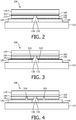
- a compliant metallization layer 210 such as gold or aluminum, may be introduced between the metal layer 150 and the interconnects 160, to act as a buffer between the metal layer 150 and the interconnects 165, to absorb some of the stress caused by thermal cycling.
- a layer 210 of softer material, such as gold or aluminum may be applied, corresponding to the pattern used to create the metal layer 150.
- This layer 210 acts as a buffer to alleviate the CTE mismatch between the metal layer 150 and the upper layers 160 and 165. It has been estimated that a 1 ⁇ m thick layer of gold may reduce the maximum principle stress within the epi-layer 150 by as much as 42%, and a 3 ⁇ m thick layer of gold can reduce the maximum principle stress within the epi-layer 150 by 49%.
- a layer of micro bumps may also be used to further enhance the compliancy of this buffer layer.
- the compliancy of the micro bump layer 145 can be reduced. Just as introducing a buffer to absorb a portion of the deformation caused by thermal cycling, reducing the compliancy of the micro bump layer will serve to restrict this distortion.
- the compliancy may be reduced, for example, by reducing the height of the micro bump layer 145, or by increasing the density or size of the micro bumps, particularly in the vicinity of the channel 135, as illustrated at 310 of FIG. 3 .
- the density of a first plurality of micro bumps arranged on each of the contacts 150 adjacent the channel 135 is greater than a density of a second plurality of micro bumps arranged on each of the contacts 150 distant from the channel 135.
- the channel areas 130 or 135 may be filled with a material that has a closer CTE to the material of the metal layer 150, thereby providing a more thermally consistent layer, reducing the distortion 190.
- the LED 100 may be overmolded with a silicone resin that molded or shaped to form a lens. Because the lens overmold material will likely flow into the channels 130 and 135, and may have a CTE around 200ppm/K, its thermal expansion will further increase the distortion of the metal layer 150 and the corresponding stress within the epi-layer 175. By filling the channel 130 on the submount side with a material with a lower CTE, the thermal expansion within the channel and the effects from this expansion will be reduced. Also, by filling the channel 135 with a material having a CTE closer to the CTE of the metal layer 150, the expansion or warping of the metal layer 150 will be reduced.
- the metal layer 150 may be structured or patterned to reduce the stress caused by thermal cycling.
- the mask used to create the metal layer 150 may include small gaps or trenches 410, i.e. un-metallized areas, that serve to redistribute the effects of the CTE mismatch between the metal layer 150 and the upper layers 160 and 165. These gaps 410 split the lateral stresses and strains that are incurred in the upper layers 160 and 165 due to the thermal expansion of the layer 150, thereby mitigating the stress at the region above the channel 135 as well.
- a computer program may be stored/distributed on a suitable medium, such as an optical storage medium or a solid-state medium supplied together with or as part of other hardware, but may also be distributed in other forms, such as via the Internet or other wired or wireless telecommunication systems. Any reference signs in the claims should not be construed as limiting the scope.
Landscapes
- Led Device Packages (AREA)
Claims (17)
- Licht emittierende Vorrichtung (100), umfassend:eine Baugruppe, aufweisend erste Kontakte (120), die durch mindestens einen ersten Kanal (130) getrennt sind,eine Licht emittierende Struktur umfassend eine Metallschicht mit zweiten Kontakten (150), wobei die zweiten Kontakte durch mindestens einen zweiten Kanal (135) getrennt sind, undeine Höckerschicht (145), die die zweiten Kontakte mit den ersten Kontakten koppelt und eine Vielzahl von Höckern einschließt,wobeidie Höcker Mikrohöcker sind, unddie Höckerschicht (145) für jeden zweiten Kontakt eine erste Vielzahl von Mikrohöckern einschließt, die in einen Bereich von jedem derartigen zweiten Kontakt benachbart dem zweiten Kanal (135) angeordnet ist, und einer zweiten Vielzahl von Mikrohöckern, die in einen Bereich von jedem derartigen zweiten Kontakt entfernt vom zweiten Kanal (135) angeordnet ist,wobei die Dichte der ersten Vielzahl von Mikrohöckern größer als eine Dichte der zweiten Vielzahl von Mikrohöckern ist, um eine thermisch induzierte Spannung in der Licht emittierenden Struktur in einer Nähe des zweiten Kanals (135) zu reduzieren.
- Licht emittierende Vorrichtung nach Anspruch 1, weiter umfassend eine Pufferschicht (210) zwischen der Metallschicht mit den zweiten Kontakten (150) und ein Licht emittierendes Element (160) in der Licht emittierenden Struktur, wobei die Pufferschicht (210) eine höhere Nachgiebigkeit als die Metallschicht mit den zweiten Kontakten (150) aufweist.
- Licht emittierende Vorrichtung nach Anspruch 2, wobei die Pufferschicht (210) Gold einschließt.
- Licht emittierende Vorrichtung nach Anspruch 1, weiter umfassend einen oder mehrere Zwischenräume (310) in der Metallschicht mit den zweiten Kontakten (150), wobei die Zwischenräume (310) angeordnet sind, um die Spannung über die Nähe des zweiten Kanals (135) hinaus zu verteilen.
- Licht emittierende Vorrichtung nach Anspruch 1, weiter umfassend ein Füllmaterial innerhalb des zweiten Kanals (135), wobei das Füllmaterial basierend auf seinem CTE ausgewählt ist.
- Licht emittierende Vorrichtung nach Anspruch 1, weiter umfassend ein Füllmaterial innerhalb des ersten Kanals (130), wobei das Füllmaterial basierend auf seinem CTE ausgewählt ist.
- Licht emittierende Vorrichtung nach Anspruch 1, wobei die Licht emittierende Struktur eine Flip-Chip-Struktur umfasst.
- Licht emittierende Vorrichtung nach Anspruch 1, wobei die Metallschicht eine Legierung umfasst.
- Licht emittierende Vorrichtung nach Anspruch 10, wobei die Legierung eine Kupferlegierung einschließt.
- Licht emittierende Vorrichtung nach Anspruch 9, wobei die Kupferlegierung mindestens eines von CuNi, CuNiTi, CuW, CuFe und CuMo einschließt.
- Licht emittierende Vorrichtung nach Anspruch 11, wobei die Kupferlegierung CuNiTi einschließt.
- Licht emittierende Vorrichtung nach Anspruch 1, wobei die Metallschicht eine Legierung einschließt, umfassend einen CTE, der geringer als ein CTE von Kupfer innerhalb eines Temperaturbereichs von 20 - 250C ist.
- Licht emittierende Vorrichtung nach Anspruch 12, wobei die Legierung eine Kupferlegierung einschließt.
- Licht emittierende Vorrichtung nach Anspruch 13, wobei die Kupferlegierung mindestens eines von CuNi, CuNiTi, CuW, CuFe und CuMo einschließt.
- Licht emittierende Vorrichtung nach Anspruch 13, wobei die Kupferlegierung CuNiTi einschließt.
- Licht emittierende Vorrichtung nach Anspruch 12, wobei die CTE der Legierung geringer als 10 ppm/K innerhalb eines Temperaturbereichs von 20 - 250C ist.
- Licht emittierende Vorrichtung nach Anspruch 12, wobei die CTE der Legierung geringer als 8 ppm/K innerhalb eines Temperaturbereichs von 20 - 250C ist.
Applications Claiming Priority (2)
| Application Number | Priority Date | Filing Date | Title |
|---|---|---|---|
| US39234910P | 2010-10-12 | 2010-10-12 | |
| PCT/IB2011/054430 WO2012049602A1 (en) | 2010-10-12 | 2011-10-07 | Light emitting device with reduced epi stress |
Publications (2)
| Publication Number | Publication Date |
|---|---|
| EP2628192A1 EP2628192A1 (de) | 2013-08-21 |
| EP2628192B1 true EP2628192B1 (de) | 2018-08-08 |
Family
ID=44906268
Family Applications (1)
| Application Number | Title | Priority Date | Filing Date |
|---|---|---|---|
| EP11778699.6A Active EP2628192B1 (de) | 2010-10-12 | 2011-10-07 | Lichtemittierende vorrichtung mit verringerter epi-belastung |
Country Status (7)
| Country | Link |
|---|---|
| US (2) | US9093630B2 (de) |
| EP (1) | EP2628192B1 (de) |
| JP (2) | JP5919284B2 (de) |
| KR (1) | KR101881178B1 (de) |
| CN (2) | CN103155183B (de) |
| TW (1) | TWI569476B (de) |
| WO (1) | WO2012049602A1 (de) |
Families Citing this family (10)
| Publication number | Priority date | Publication date | Assignee | Title |
|---|---|---|---|---|
| KR101098338B1 (ko) * | 2005-04-22 | 2011-12-26 | 삼성전자주식회사 | 광학 패키지, 광학 렌즈 및 이를 갖는 백라이트 어셈블리및 표시장치 |
| EP2628192B1 (de) | 2010-10-12 | 2018-08-08 | Lumileds Holding B.V. | Lichtemittierende vorrichtung mit verringerter epi-belastung |
| TW201320253A (zh) * | 2011-11-01 | 2013-05-16 | 華新麗華股份有限公司 | 封裝結構及其製造方法 |
| JP2014013818A (ja) * | 2012-07-04 | 2014-01-23 | Sony Corp | デバイスおよび電子装置 |
| CN104576907B (zh) * | 2014-12-18 | 2017-10-24 | 上海大学 | 倒装led芯片封装结构 |
| US10026872B2 (en) | 2015-06-05 | 2018-07-17 | Sensor Electronic Technology, Inc. | Heterostructure with stress controlling layer |
| KR102271159B1 (ko) * | 2015-10-15 | 2021-07-01 | 엘지이노텍 주식회사 | 반도체 소자, 반도체 소자 패키지, 및 이를 포함하는 조명 시스템 |
| CN106653977B (zh) * | 2017-02-24 | 2018-11-13 | 厦门多彩光电子科技有限公司 | 一种倒装芯片封装结构及成型方法 |
| CN108630645A (zh) * | 2017-03-17 | 2018-10-09 | 永道无线射频标签(扬州)有限公司 | 一种芯片和天线基材的接合结构及其制备方法 |
| JP7189441B2 (ja) * | 2019-04-17 | 2022-12-14 | 日亜化学工業株式会社 | 実装方法 |
Citations (3)
| Publication number | Priority date | Publication date | Assignee | Title |
|---|---|---|---|---|
| WO2001047039A1 (en) * | 1999-12-22 | 2001-06-28 | Lumileds Lighting, U.S., Llc | Method of making a iii-nitride light-emitting device with increased light generating capability |
| US20070267650A1 (en) * | 2006-05-17 | 2007-11-22 | Epistar Corporation | Light-emitting device |
| EP2219232A1 (de) * | 2007-11-15 | 2010-08-18 | Panasonic Corporation | Halbleiter-lichtemissionseinrichtung |
Family Cites Families (20)
| Publication number | Priority date | Publication date | Assignee | Title |
|---|---|---|---|---|
| JP3912044B2 (ja) * | 2001-06-06 | 2007-05-09 | 豊田合成株式会社 | Iii族窒化物系化合物半導体発光素子の製造方法 |
| JP4029843B2 (ja) * | 2004-01-19 | 2008-01-09 | 豊田合成株式会社 | 発光装置 |
| AU2003257713A1 (en) * | 2003-08-08 | 2005-02-25 | Vichel Inc. | Nitride micro light emitting diode with high brightness and method of manufacturing the same |
| JP2006066868A (ja) * | 2004-03-23 | 2006-03-09 | Toyoda Gosei Co Ltd | 固体素子および固体素子デバイス |
| JP4568092B2 (ja) * | 2004-11-17 | 2010-10-27 | Dowaホールディングス株式会社 | Cu−Ni−Ti系銅合金および放熱板 |
| US7125734B2 (en) * | 2005-03-09 | 2006-10-24 | Gelcore, Llc | Increased light extraction from a nitride LED |
| US7754507B2 (en) | 2005-06-09 | 2010-07-13 | Philips Lumileds Lighting Company, Llc | Method of removing the growth substrate of a semiconductor light emitting device |
| US7736945B2 (en) | 2005-06-09 | 2010-06-15 | Philips Lumileds Lighting Company, Llc | LED assembly having maximum metal support for laser lift-off of growth substrate |
| TWI394300B (zh) * | 2007-10-24 | 2013-04-21 | 榮創能源科技股份有限公司 | 光電元件之封裝結構及其製造方法 |
| US7566913B2 (en) * | 2005-12-02 | 2009-07-28 | Nitronex Corporation | Gallium nitride material devices including conductive regions and methods associated with the same |
| US20070148467A1 (en) * | 2005-12-23 | 2007-06-28 | World Properties, Inc. | Thermal management circuit materials, method of manufacture thereof, and articles formed therefrom |
| JP2007267650A (ja) * | 2006-03-30 | 2007-10-18 | Toshiba Corp | 神経毒性を検出するための方法およびキット |
| US8062925B2 (en) * | 2006-05-16 | 2011-11-22 | Koninklijke Philips Electronics N.V. | Process for preparing a semiconductor light-emitting device for mounting |
| EP2458652B1 (de) * | 2006-06-23 | 2023-08-02 | LG Electronics Inc. | Verfahren zur Herstellung lichtemittierender Dioden mit vertikaler Topologie |
| US20080149946A1 (en) * | 2006-12-22 | 2008-06-26 | Philips Lumileds Lighting Company, Llc | Semiconductor Light Emitting Device Configured To Emit Multiple Wavelengths Of Light |
| US7682959B2 (en) * | 2007-03-21 | 2010-03-23 | Stats Chippac, Ltd. | Method of forming solder bump on high topography plated Cu |
| JP2009302159A (ja) * | 2008-06-10 | 2009-12-24 | Seiko Epson Corp | 発光ダイオード装置および電子機器 |
| JP5361569B2 (ja) * | 2008-06-26 | 2013-12-04 | 京セラ株式会社 | 半導体発光素子及びその製造方法 |
| TW201010122A (en) * | 2008-08-21 | 2010-03-01 | Univ Nat Central | Flip-chip light-emitting diode having the epitaxy strengthening layer, and fabrication method thereof |
| EP2628192B1 (de) | 2010-10-12 | 2018-08-08 | Lumileds Holding B.V. | Lichtemittierende vorrichtung mit verringerter epi-belastung |
-
2011
- 2011-10-07 EP EP11778699.6A patent/EP2628192B1/de active Active
- 2011-10-07 KR KR1020137012214A patent/KR101881178B1/ko active Active
- 2011-10-07 JP JP2013533305A patent/JP5919284B2/ja active Active
- 2011-10-07 CN CN201180049451.9A patent/CN103155183B/zh active Active
- 2011-10-07 US US13/878,837 patent/US9093630B2/en active Active
- 2011-10-07 CN CN201610808930.9A patent/CN106159055B/zh active Active
- 2011-10-07 WO PCT/IB2011/054430 patent/WO2012049602A1/en not_active Ceased
- 2011-10-11 TW TW100136797A patent/TWI569476B/zh active
-
2015
- 2015-07-14 US US14/798,534 patent/US9660164B2/en active Active
-
2016
- 2016-04-11 JP JP2016078642A patent/JP6171043B2/ja active Active
Patent Citations (3)
| Publication number | Priority date | Publication date | Assignee | Title |
|---|---|---|---|---|
| WO2001047039A1 (en) * | 1999-12-22 | 2001-06-28 | Lumileds Lighting, U.S., Llc | Method of making a iii-nitride light-emitting device with increased light generating capability |
| US20070267650A1 (en) * | 2006-05-17 | 2007-11-22 | Epistar Corporation | Light-emitting device |
| EP2219232A1 (de) * | 2007-11-15 | 2010-08-18 | Panasonic Corporation | Halbleiter-lichtemissionseinrichtung |
Also Published As
| Publication number | Publication date |
|---|---|
| KR101881178B1 (ko) | 2018-07-23 |
| JP2016165002A (ja) | 2016-09-08 |
| CN106159055B (zh) | 2019-04-23 |
| CN106159055A (zh) | 2016-11-23 |
| EP2628192A1 (de) | 2013-08-21 |
| JP5919284B2 (ja) | 2016-05-18 |
| US9660164B2 (en) | 2017-05-23 |
| CN103155183A (zh) | 2013-06-12 |
| CN103155183B (zh) | 2016-10-05 |
| WO2012049602A1 (en) | 2012-04-19 |
| US9093630B2 (en) | 2015-07-28 |
| US20150318459A1 (en) | 2015-11-05 |
| JP6171043B2 (ja) | 2017-07-26 |
| JP2013539922A (ja) | 2013-10-28 |
| TWI569476B (zh) | 2017-02-01 |
| TW201222881A (en) | 2012-06-01 |
| KR20130118883A (ko) | 2013-10-30 |
| US20130193476A1 (en) | 2013-08-01 |
Similar Documents
| Publication | Publication Date | Title |
|---|---|---|
| US9660164B2 (en) | Light emitting device with reduced epi stress | |
| JP6374062B2 (ja) | マイクロledモジュール及びその製造方法 | |
| US10249604B2 (en) | Semiconductor device and method of manufacturing the same | |
| KR101765966B1 (ko) | 윈도우 삽입된 다이 패키징 | |
| US7211467B2 (en) | Method for fabricating leadless packages with mold locking characteristics | |
| CN105826281B (zh) | 扇出晶片级封装结构 | |
| US9142743B2 (en) | High temperature gold-free wafer bonding for light emitting diodes | |
| US20140332820A1 (en) | Flip Light Emitting Diode Chip and Method of Fabricating the Same | |
| KR20200050411A (ko) | 향상된 열 방산을 갖는 반도체 디바이스 및 그 제조 방법 | |
| KR100851931B1 (ko) | 반도체 패키지용의 개선된 상호접속 구조 | |
| US20160087156A1 (en) | Light emitting device | |
| US10777524B2 (en) | Using an interconnect bump to traverse through a passivation layer of a semiconductor die | |
| TW201041179A (en) | Compliant bonding structures for semiconductor devices | |
| JP2014515557A (ja) | フリップチップledのためのp−n分離メタルフィル | |
| US20160141278A1 (en) | Light emitting device | |
| CN103688372A (zh) | 用于发光二极管的凝胶层及其制造方法 | |
| TWI495160B (zh) | 覆晶式發光二極體及其製法與應用 | |
| KR20180075856A (ko) | 마이크로 엘이디 모듈 및 그 제조방법 | |
| JP2014160748A (ja) | フリップチップ型半導体素子、半導体装置及びその製造方法 | |
| CN106206908A (zh) | 具有应力减轻措施的表面安装器件 | |
| US11450794B2 (en) | Carrier and component with a buffer layer, and method for producing a component |
Legal Events
| Date | Code | Title | Description |
|---|---|---|---|
| PUAI | Public reference made under article 153(3) epc to a published international application that has entered the european phase |
Free format text: ORIGINAL CODE: 0009012 |
|
| 17P | Request for examination filed |
Effective date: 20130513 |
|
| AK | Designated contracting states |
Kind code of ref document: A1 Designated state(s): AL AT BE BG CH CY CZ DE DK EE ES FI FR GB GR HR HU IE IS IT LI LT LU LV MC MK MT NL NO PL PT RO RS SE SI SK SM TR |
|
| RAP1 | Party data changed (applicant data changed or rights of an application transferred) |
Owner name: KONINKLIJKE PHILIPS N.V. |
|
| DAX | Request for extension of the european patent (deleted) | ||
| 17Q | First examination report despatched |
Effective date: 20160729 |
|
| REG | Reference to a national code |
Ref country code: DE Ref legal event code: R079 Ref document number: 602011050863 Country of ref document: DE Free format text: PREVIOUS MAIN CLASS: H01L0033400000 Ipc: H01L0033640000 |
|
| GRAP | Despatch of communication of intention to grant a patent |
Free format text: ORIGINAL CODE: EPIDOSNIGR1 |
|
| RIC1 | Information provided on ipc code assigned before grant |
Ipc: H01L 33/64 20100101AFI20180305BHEP Ipc: H01L 33/62 20100101ALN20180305BHEP Ipc: H01L 33/40 20100101ALN20180305BHEP |
|
| INTG | Intention to grant announced |
Effective date: 20180321 |
|
| GRAS | Grant fee paid |
Free format text: ORIGINAL CODE: EPIDOSNIGR3 |
|
| GRAA | (expected) grant |
Free format text: ORIGINAL CODE: 0009210 |
|
| RAP1 | Party data changed (applicant data changed or rights of an application transferred) |
Owner name: LUMILEDS HOLDING B.V. |
|
| AK | Designated contracting states |
Kind code of ref document: B1 Designated state(s): AL AT BE BG CH CY CZ DE DK EE ES FI FR GB GR HR HU IE IS IT LI LT LU LV MC MK MT NL NO PL PT RO RS SE SI SK SM TR |
|
| REG | Reference to a national code |
Ref country code: GB Ref legal event code: FG4D |
|
| REG | Reference to a national code |
Ref country code: CH Ref legal event code: EP Ref country code: AT Ref legal event code: REF Ref document number: 1027998 Country of ref document: AT Kind code of ref document: T Effective date: 20180815 |
|
| REG | Reference to a national code |
Ref country code: IE Ref legal event code: FG4D |
|
| REG | Reference to a national code |
Ref country code: DE Ref legal event code: R096 Ref document number: 602011050863 Country of ref document: DE |
|
| REG | Reference to a national code |
Ref country code: FR Ref legal event code: PLFP Year of fee payment: 8 |
|
| REG | Reference to a national code |
Ref country code: NL Ref legal event code: MP Effective date: 20180808 |
|
| REG | Reference to a national code |
Ref country code: LT Ref legal event code: MG4D |
|
| REG | Reference to a national code |
Ref country code: AT Ref legal event code: MK05 Ref document number: 1027998 Country of ref document: AT Kind code of ref document: T Effective date: 20180808 |
|
| PG25 | Lapsed in a contracting state [announced via postgrant information from national office to epo] |
Ref country code: SE Free format text: LAPSE BECAUSE OF FAILURE TO SUBMIT A TRANSLATION OF THE DESCRIPTION OR TO PAY THE FEE WITHIN THE PRESCRIBED TIME-LIMIT Effective date: 20180808 Ref country code: BG Free format text: LAPSE BECAUSE OF FAILURE TO SUBMIT A TRANSLATION OF THE DESCRIPTION OR TO PAY THE FEE WITHIN THE PRESCRIBED TIME-LIMIT Effective date: 20181108 Ref country code: AT Free format text: LAPSE BECAUSE OF FAILURE TO SUBMIT A TRANSLATION OF THE DESCRIPTION OR TO PAY THE FEE WITHIN THE PRESCRIBED TIME-LIMIT Effective date: 20180808 Ref country code: NL Free format text: LAPSE BECAUSE OF FAILURE TO SUBMIT A TRANSLATION OF THE DESCRIPTION OR TO PAY THE FEE WITHIN THE PRESCRIBED TIME-LIMIT Effective date: 20180808 Ref country code: IS Free format text: LAPSE BECAUSE OF FAILURE TO SUBMIT A TRANSLATION OF THE DESCRIPTION OR TO PAY THE FEE WITHIN THE PRESCRIBED TIME-LIMIT Effective date: 20181208 Ref country code: PL Free format text: LAPSE BECAUSE OF FAILURE TO SUBMIT A TRANSLATION OF THE DESCRIPTION OR TO PAY THE FEE WITHIN THE PRESCRIBED TIME-LIMIT Effective date: 20180808 Ref country code: RS Free format text: LAPSE BECAUSE OF FAILURE TO SUBMIT A TRANSLATION OF THE DESCRIPTION OR TO PAY THE FEE WITHIN THE PRESCRIBED TIME-LIMIT Effective date: 20180808 Ref country code: GR Free format text: LAPSE BECAUSE OF FAILURE TO SUBMIT A TRANSLATION OF THE DESCRIPTION OR TO PAY THE FEE WITHIN THE PRESCRIBED TIME-LIMIT Effective date: 20181109 Ref country code: NO Free format text: LAPSE BECAUSE OF FAILURE TO SUBMIT A TRANSLATION OF THE DESCRIPTION OR TO PAY THE FEE WITHIN THE PRESCRIBED TIME-LIMIT Effective date: 20181108 Ref country code: FI Free format text: LAPSE BECAUSE OF FAILURE TO SUBMIT A TRANSLATION OF THE DESCRIPTION OR TO PAY THE FEE WITHIN THE PRESCRIBED TIME-LIMIT Effective date: 20180808 Ref country code: LT Free format text: LAPSE BECAUSE OF FAILURE TO SUBMIT A TRANSLATION OF THE DESCRIPTION OR TO PAY THE FEE WITHIN THE PRESCRIBED TIME-LIMIT Effective date: 20180808 |
|
| RAP2 | Party data changed (patent owner data changed or rights of a patent transferred) |
Owner name: LUMILEDS HOLDING B.V. |
|
| PG25 | Lapsed in a contracting state [announced via postgrant information from national office to epo] |
Ref country code: LV Free format text: LAPSE BECAUSE OF FAILURE TO SUBMIT A TRANSLATION OF THE DESCRIPTION OR TO PAY THE FEE WITHIN THE PRESCRIBED TIME-LIMIT Effective date: 20180808 Ref country code: AL Free format text: LAPSE BECAUSE OF FAILURE TO SUBMIT A TRANSLATION OF THE DESCRIPTION OR TO PAY THE FEE WITHIN THE PRESCRIBED TIME-LIMIT Effective date: 20180808 Ref country code: HR Free format text: LAPSE BECAUSE OF FAILURE TO SUBMIT A TRANSLATION OF THE DESCRIPTION OR TO PAY THE FEE WITHIN THE PRESCRIBED TIME-LIMIT Effective date: 20180808 |
|
| PG25 | Lapsed in a contracting state [announced via postgrant information from national office to epo] |
Ref country code: IT Free format text: LAPSE BECAUSE OF FAILURE TO SUBMIT A TRANSLATION OF THE DESCRIPTION OR TO PAY THE FEE WITHIN THE PRESCRIBED TIME-LIMIT Effective date: 20180808 Ref country code: EE Free format text: LAPSE BECAUSE OF FAILURE TO SUBMIT A TRANSLATION OF THE DESCRIPTION OR TO PAY THE FEE WITHIN THE PRESCRIBED TIME-LIMIT Effective date: 20180808 Ref country code: RO Free format text: LAPSE BECAUSE OF FAILURE TO SUBMIT A TRANSLATION OF THE DESCRIPTION OR TO PAY THE FEE WITHIN THE PRESCRIBED TIME-LIMIT Effective date: 20180808 Ref country code: CZ Free format text: LAPSE BECAUSE OF FAILURE TO SUBMIT A TRANSLATION OF THE DESCRIPTION OR TO PAY THE FEE WITHIN THE PRESCRIBED TIME-LIMIT Effective date: 20180808 Ref country code: ES Free format text: LAPSE BECAUSE OF FAILURE TO SUBMIT A TRANSLATION OF THE DESCRIPTION OR TO PAY THE FEE WITHIN THE PRESCRIBED TIME-LIMIT Effective date: 20180808 |
|
| REG | Reference to a national code |
Ref country code: DE Ref legal event code: R097 Ref document number: 602011050863 Country of ref document: DE |
|
| PG25 | Lapsed in a contracting state [announced via postgrant information from national office to epo] |
Ref country code: SK Free format text: LAPSE BECAUSE OF FAILURE TO SUBMIT A TRANSLATION OF THE DESCRIPTION OR TO PAY THE FEE WITHIN THE PRESCRIBED TIME-LIMIT Effective date: 20180808 Ref country code: DK Free format text: LAPSE BECAUSE OF FAILURE TO SUBMIT A TRANSLATION OF THE DESCRIPTION OR TO PAY THE FEE WITHIN THE PRESCRIBED TIME-LIMIT Effective date: 20180808 Ref country code: SM Free format text: LAPSE BECAUSE OF FAILURE TO SUBMIT A TRANSLATION OF THE DESCRIPTION OR TO PAY THE FEE WITHIN THE PRESCRIBED TIME-LIMIT Effective date: 20180808 |
|
| REG | Reference to a national code |
Ref country code: CH Ref legal event code: PL |
|
| PLBE | No opposition filed within time limit |
Free format text: ORIGINAL CODE: 0009261 |
|
| STAA | Information on the status of an ep patent application or granted ep patent |
Free format text: STATUS: NO OPPOSITION FILED WITHIN TIME LIMIT |
|
| REG | Reference to a national code |
Ref country code: BE Ref legal event code: MM Effective date: 20181031 |
|
| PG25 | Lapsed in a contracting state [announced via postgrant information from national office to epo] |
Ref country code: MC Free format text: LAPSE BECAUSE OF FAILURE TO SUBMIT A TRANSLATION OF THE DESCRIPTION OR TO PAY THE FEE WITHIN THE PRESCRIBED TIME-LIMIT Effective date: 20180808 Ref country code: LU Free format text: LAPSE BECAUSE OF NON-PAYMENT OF DUE FEES Effective date: 20181007 |
|
| 26N | No opposition filed |
Effective date: 20190509 |
|
| REG | Reference to a national code |
Ref country code: IE Ref legal event code: MM4A |
|
| PG25 | Lapsed in a contracting state [announced via postgrant information from national office to epo] |
Ref country code: BE Free format text: LAPSE BECAUSE OF NON-PAYMENT OF DUE FEES Effective date: 20181031 Ref country code: CH Free format text: LAPSE BECAUSE OF NON-PAYMENT OF DUE FEES Effective date: 20181031 Ref country code: SI Free format text: LAPSE BECAUSE OF FAILURE TO SUBMIT A TRANSLATION OF THE DESCRIPTION OR TO PAY THE FEE WITHIN THE PRESCRIBED TIME-LIMIT Effective date: 20180808 Ref country code: LI Free format text: LAPSE BECAUSE OF NON-PAYMENT OF DUE FEES Effective date: 20181031 |
|
| PG25 | Lapsed in a contracting state [announced via postgrant information from national office to epo] |
Ref country code: IE Free format text: LAPSE BECAUSE OF NON-PAYMENT OF DUE FEES Effective date: 20181007 |
|
| PG25 | Lapsed in a contracting state [announced via postgrant information from national office to epo] |
Ref country code: MT Free format text: LAPSE BECAUSE OF NON-PAYMENT OF DUE FEES Effective date: 20181007 |
|
| PG25 | Lapsed in a contracting state [announced via postgrant information from national office to epo] |
Ref country code: TR Free format text: LAPSE BECAUSE OF FAILURE TO SUBMIT A TRANSLATION OF THE DESCRIPTION OR TO PAY THE FEE WITHIN THE PRESCRIBED TIME-LIMIT Effective date: 20180808 |
|
| PG25 | Lapsed in a contracting state [announced via postgrant information from national office to epo] |
Ref country code: PT Free format text: LAPSE BECAUSE OF FAILURE TO SUBMIT A TRANSLATION OF THE DESCRIPTION OR TO PAY THE FEE WITHIN THE PRESCRIBED TIME-LIMIT Effective date: 20180808 |
|
| PG25 | Lapsed in a contracting state [announced via postgrant information from national office to epo] |
Ref country code: CY Free format text: LAPSE BECAUSE OF FAILURE TO SUBMIT A TRANSLATION OF THE DESCRIPTION OR TO PAY THE FEE WITHIN THE PRESCRIBED TIME-LIMIT Effective date: 20180808 Ref country code: MK Free format text: LAPSE BECAUSE OF NON-PAYMENT OF DUE FEES Effective date: 20180808 Ref country code: HU Free format text: LAPSE BECAUSE OF FAILURE TO SUBMIT A TRANSLATION OF THE DESCRIPTION OR TO PAY THE FEE WITHIN THE PRESCRIBED TIME-LIMIT; INVALID AB INITIO Effective date: 20111007 |
|
| P01 | Opt-out of the competence of the unified patent court (upc) registered |
Effective date: 20230530 |
|
| REG | Reference to a national code |
Ref country code: DE Ref legal event code: R079 Ref document number: 602011050863 Country of ref document: DE Free format text: PREVIOUS MAIN CLASS: H01L0033640000 Ipc: H10H0020858000 |
|
| PGFP | Annual fee paid to national office [announced via postgrant information from national office to epo] |
Ref country code: DE Payment date: 20251028 Year of fee payment: 15 |
|
| PGFP | Annual fee paid to national office [announced via postgrant information from national office to epo] |
Ref country code: GB Payment date: 20251023 Year of fee payment: 15 |
|
| PGFP | Annual fee paid to national office [announced via postgrant information from national office to epo] |
Ref country code: FR Payment date: 20251027 Year of fee payment: 15 |