EP2629084B1 - Circuit intégré et procédé de fabrication - Google Patents
Circuit intégré et procédé de fabrication Download PDFInfo
- Publication number
- EP2629084B1 EP2629084B1 EP12156028.8A EP12156028A EP2629084B1 EP 2629084 B1 EP2629084 B1 EP 2629084B1 EP 12156028 A EP12156028 A EP 12156028A EP 2629084 B1 EP2629084 B1 EP 2629084B1
- Authority
- EP
- European Patent Office
- Prior art keywords
- heating element
- sensing element
- metallization stack
- integrated circuit
- cavity
- Prior art date
- Legal status (The legal status is an assumption and is not a legal conclusion. Google has not performed a legal analysis and makes no representation as to the accuracy of the status listed.)
- Not-in-force
Links
Images




Classifications
-
- G—PHYSICS
- G01—MEASURING; TESTING
- G01N—INVESTIGATING OR ANALYSING MATERIALS BY DETERMINING THEIR CHEMICAL OR PHYSICAL PROPERTIES
- G01N25/00—Investigating or analyzing materials by the use of thermal means
- G01N25/18—Investigating or analyzing materials by the use of thermal means by investigating thermal conductivity
-
- H—ELECTRICITY
- H10—SEMICONDUCTOR DEVICES; ELECTRIC SOLID-STATE DEVICES NOT OTHERWISE PROVIDED FOR
- H10W—GENERIC PACKAGES, INTERCONNECTIONS, CONNECTORS OR OTHER CONSTRUCTIONAL DETAILS OF DEVICES COVERED BY CLASS H10
- H10W40/00—Arrangements for thermal protection or thermal control
-
- H—ELECTRICITY
- H10—SEMICONDUCTOR DEVICES; ELECTRIC SOLID-STATE DEVICES NOT OTHERWISE PROVIDED FOR
- H10W—GENERIC PACKAGES, INTERCONNECTIONS, CONNECTORS OR OTHER CONSTRUCTIONAL DETAILS OF DEVICES COVERED BY CLASS H10
- H10W20/00—Interconnections in chips, wafers or substrates
- H10W20/01—Manufacture or treatment
-
- H—ELECTRICITY
- H10—SEMICONDUCTOR DEVICES; ELECTRIC SOLID-STATE DEVICES NOT OTHERWISE PROVIDED FOR
- H10W—GENERIC PACKAGES, INTERCONNECTIONS, CONNECTORS OR OTHER CONSTRUCTIONAL DETAILS OF DEVICES COVERED BY CLASS H10
- H10W20/00—Interconnections in chips, wafers or substrates
- H10W20/40—Interconnections external to wafers or substrates, e.g. back-end-of-line [BEOL] metallisations or vias connecting to gate electrodes
- H10W20/498—Resistive arrangements or effects of, or between, wiring layers
-
- H—ELECTRICITY
- H10—SEMICONDUCTOR DEVICES; ELECTRIC SOLID-STATE DEVICES NOT OTHERWISE PROVIDED FOR
- H10W—GENERIC PACKAGES, INTERCONNECTIONS, CONNECTORS OR OTHER CONSTRUCTIONAL DETAILS OF DEVICES COVERED BY CLASS H10
- H10W40/00—Arrangements for thermal protection or thermal control
- H10W40/10—Arrangements for heating
Definitions
- US 5,596,219 describes a semiconductor component with monolithically integrated electronic circuits and monolithically integrated sensor/acutator, whereby the sensor/actuator is manufactured with methods of surface micromachining in a sensor layer of polysilicon that is structured, for example, with sensor webs, and these sensor webs are thermally insulated from a silicon substrate by a cavity that is produced in a sacrificial layer and is closed gas-tight toward the outside with a closure layer.
- US 2011 /0012211 A1 describes a semiconductor device comprising a stack of patterned metal layers separated by dielectric layers, said stack comprising a first conductive support structure and a second conductive support structure and a cavity in which an inertial mass element comprising at least one metal portion is conductively coupled.
- Embodiments of the present application seek to overcome at least some of the aforementioned problems.
- thermal conductivity sensor in the design of an IC without the need to sacrifice substrate area, whilst at the same providing the ability to form the conductive portion in suitable conductive materials, e.g. one or more metals.
- suitable conductive materials e.g. one or more metals.
- At least some of the semiconducting devices define a control circuit for determining the resistance of the conductive portion at a predefined voltage or current across the conductive portion such that the thermal conductivity sensor may be controlled by integrated circuits.
- Embodiments of the IC as described in this application may find their application in a wide variety of application domains, such as smart buildings, home automation, HVAC systems, supply chain monitoring, e.g. perishables in a modified atmosphere, gas monitoring in medical devices such as breathing machines and so on.
- embodiments of the IC as described in this application may be comprised in an article such as an electronic device, a vehicle, a food package, a medical apparatus such as a breathing machine and so on.
- a metallization stack is a layer structure comprising various patterned metal layers separated from each other by electrically insulating (dielectric) layers through which conductive conduits such as vias may be formed to interconnect metal portions in different layers with each other.
- a metallization stack may be used to provide the electrical interconnections between semiconductor devices in or on a substrate and/or between a semiconductor device in or on a substrate with an externally accessible contact of the IC.
- the conductive elements are formed in the upper metal layer of the metallization stack, as this requires the least amount of dielectric material to be removed from the metallization stack, thus avoiding potential issues with compromising the structural integrity of the metallization stack.
- the shape of the sensing element 16 and/or the heating element 18 is not limited to (straight) wire shapes. Any suitable shape may be contemplated. For instance, in order to increase the amount of heat transferred from the heating element 18 to the sensing element 16, an interdigitated layout as shown in layout (c), or an interdigitated meandering layout as shown in layout (d) may be chosen to increase the amount of thermal coupling between the heating element 18 and the sensing element 16.
- the metallization stack 20 comprises a metal plate 17 in a metal layer underneath the sensing element 16 and the heating element 18. Steps (a)-(c) are identical as explained with the aid of FIG. 3 .
- the metal plate 17 acts as an etch stop layer, thus preventing the uncontrolled etching in a vertical direction during the forming of cavity 36. This improves the stability of the metallization stack 20, although it cannot be avoided that the metal plate 17 will act as a heat sink, such that the sensitivity of the thermal conductivity sensor may be reduced by the presence of metal plate 17 due to the fact that less heat is transferred from the heating element 18 to the sensing element 16.
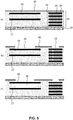
- FIG. 6 An alternative embodiment of a method of manufacturing an IC with a thermal conductivity sensor is shown in FIG. 6 .
- the sensing element 16 and the heating element 18 are formed in one of the via layers 12, more particularly formed of the material used to form the conductive conduits 24, e.g. vias.
- tungsten may be used as the via metal, which has a higher specific resistance than most metals used in the metal layers 14 of the metallization stack 20, e.g. Al or Cu, such that a higher change in resistance can be measured upon a change in temperature of the sensing element 16, which translates to a larger signal, thus increasing the sensitivity of the sensing element 16.
- steps (a)-(c) are identical as explained with the aid of FIG. 3 with the only difference being that the sensing element 16 and the heating element 18 are formed in one of the via layers 12 such as the upper via layer 12.
- the first sensing element 16, heating element 18 and further sensing element 16' are formed in the upper via layer of the metallization stack 20, although it is also feasible that the first sensing element 16, heating element 18 and further sensing element 16' are formed in a lower metal or via layer of the metallization stack 20.
- steps (a)-(c) are identical as explained with the aid of FIG. 3 with the only difference being that the heating element 18 is formed in a via layer instead of a metal layer. This may be achieved by the skilled person using routine metal layer patterning techniques such that this will not be explained in further detail for the sake of brevity only.
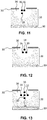
- FIG. 11-13 Some non-limiting examples of alternative embodiments of ICs having a thermal conductivity sensor in the metallization stack 20 are shown in FIG. 11-13 .
- the known fluid in the cavity 36 is displaced by the fluid of interest, which different thermal conductivity properties will cause a shift towards new equilibrium, i.e. a change in the temperature and therefore the resistance of the sensing element 18, which change is measured and translated to a reading that is indicative of or proportional to the concentration and composition of the fluid of interest, such as a gas, e.g. Ar, CH 2 O, CO 2 , CO, He, Kr, N 2 , NO 2 , N 2 O, NO, O 2 , and so on.
- a gas e.g. Ar, CH 2 O, CO 2 , CO, He, Kr, N 2 , NO 2 , N 2 O, NO, O 2 , and so on.
- IC of the present invention may further comprise additional sensors, such as relative humidity sensors, temperature sensors, ambient light sensors and so on.
Landscapes
- Physics & Mathematics (AREA)
- Health & Medical Sciences (AREA)
- Life Sciences & Earth Sciences (AREA)
- Chemical & Material Sciences (AREA)
- Analytical Chemistry (AREA)
- Biochemistry (AREA)
- General Health & Medical Sciences (AREA)
- General Physics & Mathematics (AREA)
- Immunology (AREA)
- Pathology (AREA)
- Investigating Or Analyzing Materials Using Thermal Means (AREA)
- Investigating Or Analyzing Materials By The Use Of Electric Means (AREA)
Claims (14)
- Circuit intégré comprenant un substrat (10) incluant des dispositifs semiconducteurs et un empilement de métallisation (20) sur ledit substrat pour interconnecter lesdits dispositifs, l'empilement de métallisation comprenant une cavité (36), comprenant
un détecteur de conductivité thermique comprenant au moins une paire de parties conductrices (16, 18) dudit empilement de métallisation suspendues dans ladite cavité, la paire de parties conductrices incluant un élément de détection (16) et un élément chauffant (18), et
l'élément de détection (16) étant thermiquement couplé à l'élément chauffant (18) lorsqu'il est exposé à un milieu fluide thermiquement conducteur,
sachant que, dans la cavité (36), du matériau diélectrique entourant l'élément de détection (16) et l'élément chauffant (18) a été enlevé,
l'élément de détection (16) et l'élément chauffant (18) sont séparés l'un de l'autre, et
au moins quelques-uns des dispositifs semiconducteurs définissent un circuit de commande destiné à chauffer l'élément chauffant (18) par un courant électrique et mesurer la résistance électrique de l'élément de détection (16) pour déterminer dans quelle mesure l'élément chauffant (18) a augmenté la température de l'élément de détection (16). - Le circuit intégré de la revendication 1, sachant que la paire de parties conductrices (16, 18) est formée dans une couche de métal (14) ou une couche d'interconnexion (12) de l'empilement de métallisation (20).
- Le circuit intégré de la revendication 1 ou 2, sachant que l'empilement de métallisation (20) comprend une plaque de métal (17) située entre la paire de parties conductrices (16, 18) et le substrat (10).
- Le circuit intégré de l'une des revendications 1 à 3, sachant que l'élément de détection (16) et l'élément chauffant (18) sont formés dans la même couche de l'empilement de métallisation.
- Le circuit intégré de la revendication 4, sachant que l'élément de détection (16) et l'élément chauffant (18) sont interdigités.
- Le circuit intégré de l'une des revendications 1 à 3, sachant que l'élément de détection (16) et l'élément chauffant (18) sont formés dans des couches différentes de l'empilement de métallisation (20).
- Le circuit intégré de la revendication 4 ou 6, sachant qu'au moins l'un de l'élément de détection (16) et de l'élément chauffant (18) est formé dans une couche d'interconnexion.
- Le circuit intégré de l'une quelconque des revendications 3 à 7, sachant que le détecteur de conductivité thermique comprend en outre un élément de détection supplémentaire (16') suspendu dans ladite cavité (36) à une distance de l'élément chauffant (18) qui est différente de la distance entre l'élément chauffant et l'élément de détection (16).
- Le circuit intégré de l'une quelconque des revendications 3 à 8, sachant que l'élément chauffant (18) a une forme sinueuse.
- Le circuit intégré de l'une quelconque des revendications 1 à 9, sachant que la partie conductrice (16, 18) a une forme sinueuse.
- Le circuit intégré de l'une quelconque des revendications 1 à 10, sachant que l'empilement de métallisation (20) comprend une structure de support multicouche (22) servant à supporter au moins une des parties conductrices (16, 18).
- Procédé de fabrication d'un circuit intégré comprenant un détecteur de conductivité thermique, le procédé comprenant :la fourniture d'un substrat (10) incluant une pluralité d'éléments semiconducteurs ;la formation d'un empilement de métallisation (20) sur ledit substrat pour interconnecter lesdits éléments semiconducteurs, ledit empilement de métallisation comprenant une paire de parties conductrices (16, 18) incluant un élément de détection (16) et un élément chauffant (18) séparés l'un de l'autre ;la formation d'au moins une couche de passivation (30) sur l'empilement de métallisation ;la formation d'une ouverture dans l'au moins une couche de passivation (30) au-dessus des parties conductrices (16, 18) ; etl'attaque, via l'ouverture, de la couche de passivation (30), dans l'empilement de métallisation (20), de façon à enlever ainsi du matériau diélectrique entourant l'élément de détection (16) et l'élément chauffant (18) et former une cavité (36) de telle sorte que les parties conductrices (16, 18) soient suspendues dans la cavité (36),sachant qu'au moins quelques-uns des éléments semiconducteurs définissent un circuit de commande destiné à chauffer l'élément chauffant (18) par un courant électrique et mesurer la résistance électrique de l'élément de détection (16) pour déterminer dans quelle mesure l'élément chauffant (18) a augmenté la température de l'élément de détection (16).
- Le procédé de la revendication 12, comprenant en outre :la formation de l'empilement de métallisation (20) de telle sorte qu'une plaque de métal (17) soit agencée entre les parties conductrices (16, 18) et le substrat (10) en-dessous de l'élément de détection (16) et de l'élément chauffant (18), etl'utilisation de la plaque de métal (17) comme couche d'arrêt d'attaque pendant l'attaque pour former la cavité (36).
- Le procédé de la revendication 12, sachant que l'attaque de la cavité inclut une étape d'attaque à sec épousant les formes et une recette d'attaque n'épousant pas les formes.
Priority Applications (3)
| Application Number | Priority Date | Filing Date | Title |
|---|---|---|---|
| EP12156028.8A EP2629084B1 (fr) | 2012-02-17 | 2012-02-17 | Circuit intégré et procédé de fabrication |
| US13/751,365 US8847339B2 (en) | 2012-02-17 | 2013-01-28 | Integrated circuit |
| CN201310049341.3A CN103258828B (zh) | 2012-02-17 | 2013-02-07 | 集成电路及制造方法 |
Applications Claiming Priority (1)
| Application Number | Priority Date | Filing Date | Title |
|---|---|---|---|
| EP12156028.8A EP2629084B1 (fr) | 2012-02-17 | 2012-02-17 | Circuit intégré et procédé de fabrication |
Publications (2)
| Publication Number | Publication Date |
|---|---|
| EP2629084A1 EP2629084A1 (fr) | 2013-08-21 |
| EP2629084B1 true EP2629084B1 (fr) | 2018-05-02 |
Family
ID=45656099
Family Applications (1)
| Application Number | Title | Priority Date | Filing Date |
|---|---|---|---|
| EP12156028.8A Not-in-force EP2629084B1 (fr) | 2012-02-17 | 2012-02-17 | Circuit intégré et procédé de fabrication |
Country Status (3)
| Country | Link |
|---|---|
| US (1) | US8847339B2 (fr) |
| EP (1) | EP2629084B1 (fr) |
| CN (1) | CN103258828B (fr) |
Families Citing this family (14)
| Publication number | Priority date | Publication date | Assignee | Title |
|---|---|---|---|---|
| GB201421102D0 (en) | 2014-11-27 | 2015-01-14 | Cambridge Entpr Ltd | Thermal conductivity sensing device, methods for operation and uses of the same |
| CN105675051B (zh) * | 2016-01-12 | 2018-06-05 | 上海申矽凌微电子科技有限公司 | 制造传感器集成电路的方法及使用该方法制造的集成电路 |
| CN106082102B (zh) * | 2016-07-12 | 2017-12-15 | 上海申矽凌微电子科技有限公司 | 集成温度湿度气体传感的传感器电路制造方法及传感器 |
| CN108269765B (zh) | 2016-12-30 | 2021-11-26 | 意法半导体有限公司 | 半导体传感器封装体 |
| DE102017218883A1 (de) * | 2017-10-23 | 2019-04-25 | Fraunhofer-Gesellschaft zur Förderung der angewandten Forschung e.V. | Mikroelektromechanisches Bauteil sowie ein Verfahren zu seiner Herstellung |
| DE102018006868B4 (de) * | 2018-08-30 | 2020-03-19 | Diehl Metering Gmbh | Messeinrichtung zur Ermittlung der Wärmeleitfähigkeit eines Fluids |
| EP3653567B1 (fr) | 2018-11-19 | 2024-01-10 | Sciosense B.V. | Procédé de fabrication d'un dispositif transducteur mems intégré et dispositif transducteur mems intégré |
| FR3089631B1 (fr) * | 2018-12-11 | 2024-02-02 | Commissariat Energie Atomique | Capteur de flux thermique à fil chauffant |
| EP3812753B1 (fr) * | 2019-10-24 | 2023-11-29 | Sensirion AG | Détermination de paramètres spécifiques aux gaz à partir d'un transfert de chaleur dans le régime de saut de température |
| CN111818434B (zh) * | 2020-06-30 | 2022-03-25 | 歌尔微电子有限公司 | Mems传感器和电子设备 |
| EP4521102A1 (fr) | 2021-12-17 | 2025-03-12 | Sensirion AG | Dispositif de capteur thermique et procédé de détermination de la concentration d'un gaz cible dans un échantillon de gaz |
| DE102022214190A1 (de) * | 2022-12-21 | 2024-06-27 | Vitesco Technologies GmbH | Verfahren zur Diagnose eines Gaskonzentrationssensors, Gaskonzentrationssensor, Computerprogramm und computerlesbares Medium |
| US20260023037A1 (en) * | 2024-07-18 | 2026-01-22 | Life Safety Distribution Gmbh | Thermal conductivity sensor for detecting a gas |
| CN119726113B (zh) * | 2024-12-26 | 2025-12-02 | 天津大学 | 一种基于hisl的高隔离度双极化阵列天线 |
Family Cites Families (9)
| Publication number | Priority date | Publication date | Assignee | Title |
|---|---|---|---|---|
| US4257061A (en) * | 1977-10-17 | 1981-03-17 | John Fluke Mfg. Co., Inc. | Thermally isolated monolithic semiconductor die |
| DE4418207C1 (de) * | 1994-05-25 | 1995-06-22 | Siemens Ag | Thermischer Sensor/Aktuator in Halbleitermaterial |
| US7080545B2 (en) * | 2002-10-17 | 2006-07-25 | Advanced Technology Materials, Inc. | Apparatus and process for sensing fluoro species in semiconductor processing systems |
| JP4724488B2 (ja) * | 2005-02-25 | 2011-07-13 | 日立オートモティブシステムズ株式会社 | 集積化マイクロエレクトロメカニカルシステム |
| EP1860418A1 (fr) * | 2006-05-23 | 2007-11-28 | Sensirion AG | Procédé de fabrication d'un capteur de pression utilisant les galettes de silicium SOI |
| KR20090064693A (ko) * | 2007-12-17 | 2009-06-22 | 한국전자통신연구원 | 마이크로 가스 센서 및 그 제작 방법 |
| US20100075481A1 (en) * | 2008-07-08 | 2010-03-25 | Xiao (Charles) Yang | Method and structure of monolithically integrated ic-mems oscillator using ic foundry-compatible processes |
| ATE546410T1 (de) * | 2009-07-15 | 2012-03-15 | Nxp Bv | Grenzbeschleunigungsaufnehmer und herstellungsverfahren |
| US8354729B2 (en) * | 2010-12-27 | 2013-01-15 | Industrial Technology Research Institute | Gas sensor and manufacturing method thereof |
-
2012
- 2012-02-17 EP EP12156028.8A patent/EP2629084B1/fr not_active Not-in-force
-
2013
- 2013-01-28 US US13/751,365 patent/US8847339B2/en active Active
- 2013-02-07 CN CN201310049341.3A patent/CN103258828B/zh not_active Expired - Fee Related
Non-Patent Citations (1)
| Title |
|---|
| None * |
Also Published As
| Publication number | Publication date |
|---|---|
| US8847339B2 (en) | 2014-09-30 |
| CN103258828A (zh) | 2013-08-21 |
| EP2629084A1 (fr) | 2013-08-21 |
| CN103258828B (zh) | 2016-08-03 |
| US20130214274A1 (en) | 2013-08-22 |
Similar Documents
| Publication | Publication Date | Title |
|---|---|---|
| US8847339B2 (en) | Integrated circuit | |
| JP5736400B2 (ja) | ガスセンサを有する集積回路 | |
| US10094797B2 (en) | Integrated multi-sensor module | |
| US7471093B2 (en) | Capacitive humidity sensor | |
| EP2720034B1 (fr) | Circuit intégré comprenant un capteur d'humidite relaitive et un capteur de gaz basé sur la conductivité thermique | |
| EP2554981B1 (fr) | Circuit intégré avec un capteur de gaz et procédé de fabrication d'un tel circuit intégré | |
| US6906392B2 (en) | Micromechanical component | |
| US9766195B2 (en) | Integrated circuit with sensor and method of manufacturing such an integrated circuit | |
| US7255001B1 (en) | Thermal fluid flow sensor and method of forming same technical field | |
| TWI630169B (zh) | 製造微機電系統裝置的方法 | |
| WO2008046867A1 (fr) | Résistance métallique encapsulée | |
| US8528397B2 (en) | Hermeticity sensor and related method | |
| KR101024616B1 (ko) | 기울기 또는 가속도 측정이 가능한 반도체 센서 및 그의 제조방법 | |
| TWI601944B (zh) | Thermal pressure sensor manufacturing process | |
| KR100650603B1 (ko) | 응축방울 검지센서 | |
| JP2013003068A (ja) | 流量センサ | |
| CN102336391A (zh) | 用于制造压阻的传感器装置的方法以及传感器装置 |
Legal Events
| Date | Code | Title | Description |
|---|---|---|---|
| PUAI | Public reference made under article 153(3) epc to a published international application that has entered the european phase |
Free format text: ORIGINAL CODE: 0009012 |
|
| AK | Designated contracting states |
Kind code of ref document: A1 Designated state(s): AL AT BE BG CH CY CZ DE DK EE ES FI FR GB GR HR HU IE IS IT LI LT LU LV MC MK MT NL NO PL PT RO RS SE SI SK SM TR |
|
| AX | Request for extension of the european patent |
Extension state: BA ME |
|
| 17P | Request for examination filed |
Effective date: 20131031 |
|
| RBV | Designated contracting states (corrected) |
Designated state(s): AL AT BE BG CH CY CZ DE DK EE ES FI FR GB GR HR HU IE IS IT LI LT LU LV MC MK MT NL NO PL PT RO RS SE SI SK SM TR |
|
| 17Q | First examination report despatched |
Effective date: 20150904 |
|
| RAP1 | Party data changed (applicant data changed or rights of an application transferred) |
Owner name: AMS INTERNATIONAL AG |
|
| GRAP | Despatch of communication of intention to grant a patent |
Free format text: ORIGINAL CODE: EPIDOSNIGR1 |
|
| STAA | Information on the status of an ep patent application or granted ep patent |
Free format text: STATUS: GRANT OF PATENT IS INTENDED |
|
| INTG | Intention to grant announced |
Effective date: 20171222 |
|
| GRAS | Grant fee paid |
Free format text: ORIGINAL CODE: EPIDOSNIGR3 |
|
| GRAA | (expected) grant |
Free format text: ORIGINAL CODE: 0009210 |
|
| STAA | Information on the status of an ep patent application or granted ep patent |
Free format text: STATUS: THE PATENT HAS BEEN GRANTED |
|
| AK | Designated contracting states |
Kind code of ref document: B1 Designated state(s): AL AT BE BG CH CY CZ DE DK EE ES FI FR GB GR HR HU IE IS IT LI LT LU LV MC MK MT NL NO PL PT RO RS SE SI SK SM TR |
|
| REG | Reference to a national code |
Ref country code: GB Ref legal event code: FG4D |
|
| REG | Reference to a national code |
Ref country code: CH Ref legal event code: EP Ref country code: AT Ref legal event code: REF Ref document number: 995808 Country of ref document: AT Kind code of ref document: T Effective date: 20180515 |
|
| REG | Reference to a national code |
Ref country code: DE Ref legal event code: R096 Ref document number: 602012045807 Country of ref document: DE |
|
| REG | Reference to a national code |
Ref country code: IE Ref legal event code: FG4D |
|
| REG | Reference to a national code |
Ref country code: NL Ref legal event code: MP Effective date: 20180502 |
|
| REG | Reference to a national code |
Ref country code: LT Ref legal event code: MG4D |
|
| PG25 | Lapsed in a contracting state [announced via postgrant information from national office to epo] |
Ref country code: ES Free format text: LAPSE BECAUSE OF FAILURE TO SUBMIT A TRANSLATION OF THE DESCRIPTION OR TO PAY THE FEE WITHIN THE PRESCRIBED TIME-LIMIT Effective date: 20180502 Ref country code: LT Free format text: LAPSE BECAUSE OF FAILURE TO SUBMIT A TRANSLATION OF THE DESCRIPTION OR TO PAY THE FEE WITHIN THE PRESCRIBED TIME-LIMIT Effective date: 20180502 Ref country code: BG Free format text: LAPSE BECAUSE OF FAILURE TO SUBMIT A TRANSLATION OF THE DESCRIPTION OR TO PAY THE FEE WITHIN THE PRESCRIBED TIME-LIMIT Effective date: 20180802 Ref country code: FI Free format text: LAPSE BECAUSE OF FAILURE TO SUBMIT A TRANSLATION OF THE DESCRIPTION OR TO PAY THE FEE WITHIN THE PRESCRIBED TIME-LIMIT Effective date: 20180502 Ref country code: NO Free format text: LAPSE BECAUSE OF FAILURE TO SUBMIT A TRANSLATION OF THE DESCRIPTION OR TO PAY THE FEE WITHIN THE PRESCRIBED TIME-LIMIT Effective date: 20180802 Ref country code: SE Free format text: LAPSE BECAUSE OF FAILURE TO SUBMIT A TRANSLATION OF THE DESCRIPTION OR TO PAY THE FEE WITHIN THE PRESCRIBED TIME-LIMIT Effective date: 20180502 |
|
| PG25 | Lapsed in a contracting state [announced via postgrant information from national office to epo] |
Ref country code: GR Free format text: LAPSE BECAUSE OF FAILURE TO SUBMIT A TRANSLATION OF THE DESCRIPTION OR TO PAY THE FEE WITHIN THE PRESCRIBED TIME-LIMIT Effective date: 20180803 Ref country code: RS Free format text: LAPSE BECAUSE OF FAILURE TO SUBMIT A TRANSLATION OF THE DESCRIPTION OR TO PAY THE FEE WITHIN THE PRESCRIBED TIME-LIMIT Effective date: 20180502 Ref country code: LV Free format text: LAPSE BECAUSE OF FAILURE TO SUBMIT A TRANSLATION OF THE DESCRIPTION OR TO PAY THE FEE WITHIN THE PRESCRIBED TIME-LIMIT Effective date: 20180502 Ref country code: HR Free format text: LAPSE BECAUSE OF FAILURE TO SUBMIT A TRANSLATION OF THE DESCRIPTION OR TO PAY THE FEE WITHIN THE PRESCRIBED TIME-LIMIT Effective date: 20180502 Ref country code: NL Free format text: LAPSE BECAUSE OF FAILURE TO SUBMIT A TRANSLATION OF THE DESCRIPTION OR TO PAY THE FEE WITHIN THE PRESCRIBED TIME-LIMIT Effective date: 20180502 |
|
| REG | Reference to a national code |
Ref country code: AT Ref legal event code: MK05 Ref document number: 995808 Country of ref document: AT Kind code of ref document: T Effective date: 20180502 |
|
| PG25 | Lapsed in a contracting state [announced via postgrant information from national office to epo] |
Ref country code: CZ Free format text: LAPSE BECAUSE OF FAILURE TO SUBMIT A TRANSLATION OF THE DESCRIPTION OR TO PAY THE FEE WITHIN THE PRESCRIBED TIME-LIMIT Effective date: 20180502 Ref country code: SK Free format text: LAPSE BECAUSE OF FAILURE TO SUBMIT A TRANSLATION OF THE DESCRIPTION OR TO PAY THE FEE WITHIN THE PRESCRIBED TIME-LIMIT Effective date: 20180502 Ref country code: EE Free format text: LAPSE BECAUSE OF FAILURE TO SUBMIT A TRANSLATION OF THE DESCRIPTION OR TO PAY THE FEE WITHIN THE PRESCRIBED TIME-LIMIT Effective date: 20180502 Ref country code: PL Free format text: LAPSE BECAUSE OF FAILURE TO SUBMIT A TRANSLATION OF THE DESCRIPTION OR TO PAY THE FEE WITHIN THE PRESCRIBED TIME-LIMIT Effective date: 20180502 Ref country code: DK Free format text: LAPSE BECAUSE OF FAILURE TO SUBMIT A TRANSLATION OF THE DESCRIPTION OR TO PAY THE FEE WITHIN THE PRESCRIBED TIME-LIMIT Effective date: 20180502 Ref country code: RO Free format text: LAPSE BECAUSE OF FAILURE TO SUBMIT A TRANSLATION OF THE DESCRIPTION OR TO PAY THE FEE WITHIN THE PRESCRIBED TIME-LIMIT Effective date: 20180502 Ref country code: AT Free format text: LAPSE BECAUSE OF FAILURE TO SUBMIT A TRANSLATION OF THE DESCRIPTION OR TO PAY THE FEE WITHIN THE PRESCRIBED TIME-LIMIT Effective date: 20180502 |
|
| REG | Reference to a national code |
Ref country code: DE Ref legal event code: R097 Ref document number: 602012045807 Country of ref document: DE |
|
| PG25 | Lapsed in a contracting state [announced via postgrant information from national office to epo] |
Ref country code: SM Free format text: LAPSE BECAUSE OF FAILURE TO SUBMIT A TRANSLATION OF THE DESCRIPTION OR TO PAY THE FEE WITHIN THE PRESCRIBED TIME-LIMIT Effective date: 20180502 Ref country code: IT Free format text: LAPSE BECAUSE OF FAILURE TO SUBMIT A TRANSLATION OF THE DESCRIPTION OR TO PAY THE FEE WITHIN THE PRESCRIBED TIME-LIMIT Effective date: 20180502 |
|
| PLBE | No opposition filed within time limit |
Free format text: ORIGINAL CODE: 0009261 |
|
| STAA | Information on the status of an ep patent application or granted ep patent |
Free format text: STATUS: NO OPPOSITION FILED WITHIN TIME LIMIT |
|
| 26N | No opposition filed |
Effective date: 20190205 |
|
| PG25 | Lapsed in a contracting state [announced via postgrant information from national office to epo] |
Ref country code: SI Free format text: LAPSE BECAUSE OF FAILURE TO SUBMIT A TRANSLATION OF THE DESCRIPTION OR TO PAY THE FEE WITHIN THE PRESCRIBED TIME-LIMIT Effective date: 20180502 |
|
| REG | Reference to a national code |
Ref country code: CH Ref legal event code: PL |
|
| GBPC | Gb: european patent ceased through non-payment of renewal fee |
Effective date: 20190217 |
|
| PG25 | Lapsed in a contracting state [announced via postgrant information from national office to epo] |
Ref country code: MC Free format text: LAPSE BECAUSE OF FAILURE TO SUBMIT A TRANSLATION OF THE DESCRIPTION OR TO PAY THE FEE WITHIN THE PRESCRIBED TIME-LIMIT Effective date: 20180502 Ref country code: LU Free format text: LAPSE BECAUSE OF NON-PAYMENT OF DUE FEES Effective date: 20190217 |
|
| REG | Reference to a national code |
Ref country code: BE Ref legal event code: MM Effective date: 20190228 |
|
| REG | Reference to a national code |
Ref country code: IE Ref legal event code: MM4A |
|
| PG25 | Lapsed in a contracting state [announced via postgrant information from national office to epo] |
Ref country code: AL Free format text: LAPSE BECAUSE OF FAILURE TO SUBMIT A TRANSLATION OF THE DESCRIPTION OR TO PAY THE FEE WITHIN THE PRESCRIBED TIME-LIMIT Effective date: 20180502 |
|
| PG25 | Lapsed in a contracting state [announced via postgrant information from national office to epo] |
Ref country code: LI Free format text: LAPSE BECAUSE OF NON-PAYMENT OF DUE FEES Effective date: 20190228 Ref country code: CH Free format text: LAPSE BECAUSE OF NON-PAYMENT OF DUE FEES Effective date: 20190228 |
|
| PG25 | Lapsed in a contracting state [announced via postgrant information from national office to epo] |
Ref country code: IE Free format text: LAPSE BECAUSE OF NON-PAYMENT OF DUE FEES Effective date: 20190217 Ref country code: GB Free format text: LAPSE BECAUSE OF NON-PAYMENT OF DUE FEES Effective date: 20190217 |
|
| PG25 | Lapsed in a contracting state [announced via postgrant information from national office to epo] |
Ref country code: FR Free format text: LAPSE BECAUSE OF NON-PAYMENT OF DUE FEES Effective date: 20190228 Ref country code: BE Free format text: LAPSE BECAUSE OF NON-PAYMENT OF DUE FEES Effective date: 20190228 |
|
| PG25 | Lapsed in a contracting state [announced via postgrant information from national office to epo] |
Ref country code: TR Free format text: LAPSE BECAUSE OF FAILURE TO SUBMIT A TRANSLATION OF THE DESCRIPTION OR TO PAY THE FEE WITHIN THE PRESCRIBED TIME-LIMIT Effective date: 20180502 |
|
| PG25 | Lapsed in a contracting state [announced via postgrant information from national office to epo] |
Ref country code: PT Free format text: LAPSE BECAUSE OF FAILURE TO SUBMIT A TRANSLATION OF THE DESCRIPTION OR TO PAY THE FEE WITHIN THE PRESCRIBED TIME-LIMIT Effective date: 20180903 Ref country code: MT Free format text: LAPSE BECAUSE OF NON-PAYMENT OF DUE FEES Effective date: 20190217 |
|
| PG25 | Lapsed in a contracting state [announced via postgrant information from national office to epo] |
Ref country code: CY Free format text: LAPSE BECAUSE OF FAILURE TO SUBMIT A TRANSLATION OF THE DESCRIPTION OR TO PAY THE FEE WITHIN THE PRESCRIBED TIME-LIMIT Effective date: 20180502 |
|
| PG25 | Lapsed in a contracting state [announced via postgrant information from national office to epo] |
Ref country code: IS Free format text: LAPSE BECAUSE OF FAILURE TO SUBMIT A TRANSLATION OF THE DESCRIPTION OR TO PAY THE FEE WITHIN THE PRESCRIBED TIME-LIMIT Effective date: 20180902 |
|
| PG25 | Lapsed in a contracting state [announced via postgrant information from national office to epo] |
Ref country code: HU Free format text: LAPSE BECAUSE OF FAILURE TO SUBMIT A TRANSLATION OF THE DESCRIPTION OR TO PAY THE FEE WITHIN THE PRESCRIBED TIME-LIMIT; INVALID AB INITIO Effective date: 20120217 |
|
| PGFP | Annual fee paid to national office [announced via postgrant information from national office to epo] |
Ref country code: DE Payment date: 20220217 Year of fee payment: 11 |
|
| PG25 | Lapsed in a contracting state [announced via postgrant information from national office to epo] |
Ref country code: MK Free format text: LAPSE BECAUSE OF FAILURE TO SUBMIT A TRANSLATION OF THE DESCRIPTION OR TO PAY THE FEE WITHIN THE PRESCRIBED TIME-LIMIT Effective date: 20180502 |
|
| REG | Reference to a national code |
Ref country code: DE Ref legal event code: R119 Ref document number: 602012045807 Country of ref document: DE |
|
| P01 | Opt-out of the competence of the unified patent court (upc) registered |
Effective date: 20230821 |
|
| PG25 | Lapsed in a contracting state [announced via postgrant information from national office to epo] |
Ref country code: DE Free format text: LAPSE BECAUSE OF NON-PAYMENT OF DUE FEES Effective date: 20230901 |