EP2629102A2 - Circuit optique intégré et procédé de mesure de courant ainsi que module de capteur et dispositif de mesure - Google Patents
Circuit optique intégré et procédé de mesure de courant ainsi que module de capteur et dispositif de mesure Download PDFInfo
- Publication number
- EP2629102A2 EP2629102A2 EP13000143.1A EP13000143A EP2629102A2 EP 2629102 A2 EP2629102 A2 EP 2629102A2 EP 13000143 A EP13000143 A EP 13000143A EP 2629102 A2 EP2629102 A2 EP 2629102A2
- Authority
- EP
- European Patent Office
- Prior art keywords
- optical
- waveguide
- integrated
- coupled
- circuit according
- Prior art date
- Legal status (The legal status is an assumption and is not a legal conclusion. Google has not performed a legal analysis and makes no representation as to the accuracy of the status listed.)
- Withdrawn
Links
Images




Classifications
-
- G—PHYSICS
- G01—MEASURING; TESTING
- G01R—MEASURING ELECTRIC VARIABLES; MEASURING MAGNETIC VARIABLES
- G01R15/00—Details of measuring arrangements of the types provided for in groups G01R17/00 - G01R29/00, G01R33/00 - G01R33/26 or G01R35/00
- G01R15/14—Adaptations providing voltage or current isolation, e.g. for high-voltage or high-current networks
- G01R15/24—Adaptations providing voltage or current isolation, e.g. for high-voltage or high-current networks using light-modulating devices
- G01R15/245—Adaptations providing voltage or current isolation, e.g. for high-voltage or high-current networks using light-modulating devices using magneto-optical modulators, e.g. based on the Faraday or Cotton-Mouton effect
- G01R15/246—Adaptations providing voltage or current isolation, e.g. for high-voltage or high-current networks using light-modulating devices using magneto-optical modulators, e.g. based on the Faraday or Cotton-Mouton effect based on the Faraday, i.e. linear magneto-optic, effect
Definitions
- the invention relates to an integrated optical circuit for measuring current based on the Faraday effect, a sensor module with such an integrated optical circuit and a measuring device.
- the invention further relates to a method for current measurement by means of an integrated optical circuit.
- Fiber-optic current sensors detect the current through a conductor by means of a fiber wound around the conductor.
- the magnetic field surrounding the conductor rotates the light oscillation plane of linearly polarized light or causes a phase shift between mutually orthogonal circular polarization modes of a light beam guided through the optical fiber.
- the amount of phase shift between polarization modes caused by the electrical current is a measure of the current in the conductor.
- a light beam generated by a light source is guided via a directional coupler to a polarizer and linearly polarized by the polarizer.
- the polarized light is coupled by means of a fiber splice at 45 degrees against the polarization axes of a polarization-maintaining fiber, so that in the same fiber two different polarization modes are performed in parallel with approximately the same amplitude.
- the two polarization modes are parallel-guided "partial light beams" of a primary light beam having a defined polarization and each use a different optical light path in the polarization-maintaining fiber.
- the two polarization modes pass through a birefringence phase modulator, which sets a non-reciprocal phase shift between the two polarization modes.
- a ⁇ / 4 phase shifter converts the linearly polarized light into circularly polarized light to enhance the effect of the Faraday effect.
- the light passes through a fiber coil which wraps around the conductor with the current to be measured, and is reflected in a reflector. If a current flows in the conductor, the Faraday effect between the two circularly polarized polarization modes causes a phase shift whose magnitude is proportional to the current in the conductor.
- the returning polarization modes are combined at the fiber splice and passed over the polarizer and the directional coupler to a detector on which the two polarization modes interfere. The phase shift is reflected in a shift of the interference pattern that is evaluated.
- the present invention has for its object to provide a measuring device for current measurement based on the Faraday effect available, which is inexpensive to manufacture.
- the object is solved by the subject matter of the independent claims. Advantageous developments emerge from the subclaims.
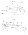
- the Figure 1A shows a schematic plan view of an optical module of an integrated optical circuit.
- FIG. 1B shows a schematic representation of a measuring device for measuring a current based on the Faraday effect by means of a single integrated optical circuit with the optical module Figure 1A ,
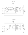
- FIG. 2A shows a schematic plan view of an integrated optical circuit with an optical module according to an embodiment having a waveguide-Kombinierelement and a waveguide branching element.
- FIG. 2B shows a schematic plan view of an integrated optical circuit according to an embodiment with an optical module with a 2: 2 directional coupling element.
- FIG. 3 shows a schematic plan view of a sensor module with an integrated optical circuit, a light source, a detector element and an evaluation and control unit according to a hybrid embodiment.
- FIG. 4 shows a schematic plan view of a sensor module with an integrated optical circuit, are monolithically integrated in the light source, detector element and evaluation and control unit.
- FIG. 5A shows a schematic plan view of a space filter element for an integrated optical circuit according to an embodiment with a single bend.
- FIG. 5B shows a schematic plan view of a spatial filter element according to an embodiment with a double bend.
- FIG. 5C shows a schematic plan view of a spatial filter element according to an embodiment with a cross-sectional constriction of a strip waveguide.
- FIG. 5D shows a schematic plan view of a spatial filter element according to an embodiment with different waveguide geometries.
- FIG. 6 shows a schematic plan view of an integrated optical circuit with three optical modules for measuring three-phase currents.
- FIG. 7 shows a schematic representation of a measuring device for measuring three-phase currents by means of the integrated optical circuit according to FIG. 6 .
- FIG. 8 shows a schematic plan view of an integrated optical circuit comprising a 1: 3 coupler and three 2: 2 coupler for measuring three-phase currents.
- FIG. 9 is a simplified flowchart for a method of operating a measuring device.
- the Figure 1A shows an integrated optical circuit 100 for current measurement based on the Faraday effect.
- the integrated optical circuit 100 has one or more measurement modules 101.
- Each measuring module 101 comprises a first strip waveguide 141 and a second strip waveguide 142.
- the material of the strip waveguides 141, 142 is polarization-maintaining.
- the material of the strip waveguides 141, 142 is a highly anisotropic, polarizing material.
- the material of the strip waveguides 141, 142 is a semiconductor material, for example GaAs or silicon.
- the stripe waveguides 141, 142 may each be wholly or partially exposed as ridge waveguides resting on a lower refractive index substrate, as buried ridge waveguides embedded in a lower refractive index substrate, as a slotted waveguide, or as a nano-ridge waveguide (nano rib waveguide) be executed.
- the substrate underlying the strip waveguides 141, 142 is, for example, monocrystalline silicon, silicon dioxide or glass.
- the width of the strip waveguides 141, 142 is 100 microns or less. According to one embodiment, the width is on the order of or smaller than the wavelength of the light guided in the strip waveguides 141, 142.
- the width of the strip waveguides 141, 142 is at most in sections at most 1 micrometer or at most 300 nm.
- the integrated optical circuit 100 further includes a waveguide coupling element 160.
- the waveguide coupling element 160 couples both the light signal supplied via the first strip waveguide 141 and the second strip waveguide 142 to an optical fiber line 202.
- the waveguide coupling element 160 couples the two light signals to different polarization modes of the optical fiber line 202. Conversely, it couples two orthogonal polarization modes of a light beam brought in via the optical fiber line 202 depending on the polarization direction on either the first strip waveguide 141 or the second strip waveguide 142.
- the waveguide coupling element 160 is for example a decoupling grating and an end face of the optical fiber line 202 is substantially parallel to the grating surface aligned above the decoupling grid arranged.
- the coupling-out grating couples the two optical signals brought in via the two strip waveguides 141, 142 into orthogonal linear polarization states of the optical fiber line 202.
- the coupling-out grating is, for example, a two-dimensional grating in an overlapping region of the first and second strip waveguides 141, 142.
- the dimensions of the coupling-out grid can be adapted to the cross section of the fiber line.
- the decoupling grid may comprise an area of less than 1 mm 2 .
- the edge length can be between several tens and several hundreds of micrometers.
- the two strip waveguides 141, 142 intersect, for example, in the decoupling grid at an angle of 90 degrees.
- the width of the strip waveguides 141, 142 can be adjusted continuously or linearly in a transition section starting from a width of several tens or hundreds of nanometers to the edge length of the coupling-out grid.
- the grating is etched into a silicon layer several to several 100 nm thick, which rests on an SiO 2 layer.
- the grid includes a regular array of wells having a depth of 90 nm and a diameter of the wells of about 300 nm at a grating period of 580 nm.
- the integrated optical circuit 100 further comprises a phase modulator device 150 via which a phase difference between the two light signals of the same polarization in the first and second strip waveguides 141, 142 can be controlled.
- the optical module 101 has one or more electrical leads 153, which are guided between an electrical interface 154 of the optical module 101 and the phase modulator device 150.
- a directional coupling element 130 branches off the two optical light signals guided via the two strip waveguides 141, 142 to the optical fiber line 202 from a common optical input signal and also combines the two optical partial signals received from the optical fiber line 202 into a common output signal.
- Another strip waveguide 113 connects the directional coupling element 130 to an input port 111, via which the optical input signal is coupled into the optical module 101.
- the optical output signal is output via an output port 121, which is connected via a further strip waveguide 123 to the directional coupling element 130.
- the phase modulator device 150 may be, for example, a push-pull type electro-optic phase modulator.
- the phase modulator device 150 comprises exactly one modulator unit in each of the two optical signal paths with the first and second strip waveguides 141, 142. Since the phase modulator device 150 ultimately only the phase difference between the two optical signals in the two by the first and second strip waveguide 141, 142 defines defined optical signal paths, the phase modulator device 150 in another embodiment comprises exactly one modulator unit in one of the two optical signal paths.
- Each modulator unit can be integral.
- at least one of the modulator units is segmented, wherein the segments can be controlled independently of one another.
- one of the segments can be used to set a fixed phase offset and thus a certain operating point, while another segment is used predominantly or exclusively for the high-frequency modulation of the measurement signal.
- a plurality of segments of a modulator unit are designed in the manner of a digital phase modulator (optical DA converter).
- the directional coupling element 130 is, for example, an integrated-optical 2: 2 directional coupler with a phase difference of 90 ° C between the two output-side optical signals.
- the directional coupling element 130 feeds an optical input signal at a first port of a first pair of ports to a first or second port of a second pair of ports and optical signals at the gates of the second pair of ports to the second port of the first pair of ports.
- the directional coupling element 130 guides an input optical signal to the first and second ridge waveguides 141, 142.
- the directional coupling element 130 couples the optical sub-signals received from the optical fiber line 202 and coupled to the first and second ridge waveguides 141, 142 on the strip waveguide 123, which is connected to the output port 121 of the optical module 101.
- a first optical signal path with the first strip waveguide 141 between the first port of the second pair of ports of the directional coupling element 130 and the waveguide coupling element 160 has a different optical path than the second optical signal path with the second strip waveguide 142 between the second port of the second pair of ports of the directional coupling element 130 and the waveguide coupling element 160.
- the optical path difference causes an interference contrast of the optical signals in the waveguide coupling element 160 to be reduced or nearly zero by at least 50%, for example 90% or more, compared to an imaginary design with identical path lengths.
- the optical path difference results from the bandwidth of the optical signal and the effective refractive index of the strip waveguide. According to an embodiment for a Si waveguide with an effective refractive index of about 3 and a wavelength difference ⁇ of 30 nm at a significant wavelength of 1500 nm, the optical path difference is about 100 ⁇ m.
- the integrated optical circuit 100 With the integrated optical circuit 100, the number of necessary fiber splices and thus the number of potential polarization cross coupling points, which can lead to inaccuracies in the sensor, can be significantly reduced. In addition, the integrated optical circuit 100 can be manufactured comparatively easily.
- the FIG. 1B shows a measuring device for measuring the magnetic field or for measuring a current through a line 900 by means of the described integrated optical circuit with an optical module 101.
- the input port 111 Via the input port 111, light of a light source 110 is fed to an integrated optical circuit having an optical module 101.
- the light In the optical circuit, the light is polarized and coupled to two optical signal paths of different path length. Of the two optical signal paths, the two sub-signals are coupled to different polarization modes of an optical fiber line 202.
- the optical fiber line 202 thus performs an optical signal consisting of two sub-signals with different linear polarization and phase.
- the two polarization modes pass through a delay element 210 to a ⁇ / 4 plate 220 (quarter-wave length plate), which converts the two linearly polarized light waves in a left circular and a right circularly polarized light wave.
- the optical signal passes through an optical fiber coil 310 which wraps around a current carrying conductor 900.
- a reflector 320 at the end of the fiber coil 310 reflects the optical signal.
- the two circular polarization modes of the reflected signal are converted again into linearly polarized polarization modes in the ⁇ / 4 plate 220 and are coupled into the optical module 101 via the optical fiber line 202.
- the optical module 101 generates from the two polarization modes, two optical sub-signals of the same polarization mode, combines these and performs the combination signal with the two optical sub-signals to a detector element 120 which is coupled to the output port 121 of the optical module 101.
- the detector element 126 registers the phase difference between the two optical sub-signals.
- An evaluation and control unit 180 evaluates a phase difference between the two sub-signals in order to control a phase modulation device in the optical module 101 via an electrical interface 154 in such a way that the phase difference between the two optical sub-signals does not deviate from a predefined value.
- the FIG. 2A refers to an embodiment in which the directional coupler comprises a waveguide combiner 132 and a waveguide manifold 138.
- the waveguide combining element 132 applies optical signals at the first and second ports of the first pair of ports to a third band waveguide 133 and an optical signal from the third band waveguide 133 to the second port of the first pair of ports.
- the waveguide branching element 138 couples the signal from the third ridge waveguide 133 in equal parts to the first and second optical signal paths with the first and second ridge waveguides 141, 142 and couples the optical sub-signals received from the optical fiber line 202 from the first and second optical paths Signal path to the third stripe waveguide 133.
- the waveguide combining element 132 and the waveguide branching element 138 are, for example, Y-type stripe structures in the technology of the strip waveguides 141, 142, 133 provided in the optical module 101.
- the directional coupling element may comprise a polarization element 134 which linearly polarizes light.
- the polarization element 134 is an integrated-optical polarizer, for example of the plasmon type, wherein a thin-film system comprising at least one dielectric layer and one metal layer is provided above a silicon nanowave conductor. By excitation of a plasmon in the metal layer, a polarization mode guided in the silicon nanowave conductor is quasi absorbed.
- the polarization element 134 is a hybrid-integrated polarizer, such as a thin-film polarizer, for example a glass polarizer having a thickness of 10 to several 100 ⁇ m, disposed in a trench which is inserted into the substrate, e.g. a silicon substrate was etched. If already polarized light is fed into the optical module 101 or if the strip waveguides themselves are polarizing, then the polarization element 134 can be dispensed with.
- integrated silicon nanowires have a strong polarization dependence, i. The two linearly polarized eigenmodes have very different propagation constants, so that the polarization states are strongly decoupled from each other.
- the silicon nanowave conductors can be designed such that only one of the two linearly polarized eigenmodes is capable of propagation at all, so that the integrated silicon nanowave conductor itself is effective as a polarizer.
- the polarizing effect of the silicon nanowave conductor or the polarization element 134 ensure that only a linear polarization is guided and modulated in the interferometer.
- the optical module 101 may include a spatial filter element 136 disposed in the optical path between the waveguide combining element 132 and the waveguide branching element 138, a spatial filter element 136.
- the spatial filter element 136 suppresses non-reciprocal light paths that arise in the otherwise reciprocal integrated-optical interferometer by excitation of a second or higher waveguide mode. Such a second waveguide mode can be excited, for example, in the waveguide branch element 138.
- the corresponding optical fiber has a minimum length at which such a higher mode completely radiates. When implemented in an integrated-optical circuit, however, the length of the corresponding section of the strip waveguide is insufficient. Instead, one embodiment provides a spatial filter element 136 between the waveguide combiner 132 and the waveguide manifold 138.
- the optical module 101 includes a first modulator unit 151, which operates in a first optical path with the first ridge waveguide 141, and a second modulator unit 152, which operates in a second optical path with the second ridge waveguide 142.
- the FIG. 2B refers to an embodiment with a 2: 2 directional coupler 139 as a directional coupling element.
- the ridge waveguides of the integrated optical circuit 100 are designed such that only one of the two linearly polarized eigenmodes is capable of propagation, as is the case, for example, with a highly anisotropic waveguide.
- the eigenmode can be, for example, the TE mode, in which the electric field is oriented essentially parallel to the substrate plane.
- Such a solution does not require an integrated optical polarizer.
- the light emitted by a light source and input via the input port 111 is split by the 2: 2 directional coupler 139 onto two arms of an interferometer arrangement.
- a phase modulator device with two module units 151, 152 modulates the phase difference between the optical signals in the two arms.
- the two optical signals are coupled through a waveguide coupling element 160 into orthogonal, linear states of polarization of an optical fiber line 202.
- the FIG. 3 refers to a sensor module 201 with an integrated optical circuit 100 that includes only one optical module 101.
- the light emitted by a light source 110 is coupled via an input port 1 11 in the optical module 101 of the integrated optical circuit 100, passed through a waveguide Kombinierelement 132 on a polarizing element 134, there linearly polarized and by a waveguide branching element 138 on two asymmetric Strip waveguide 141, 142 distributed, wherein the waveguide branch element 138 can produce a phase difference between the guided in the two strip waveguides 141, 142 optical signals.
- the two strip waveguides 141, 142 are brought together in a waveguide coupling element 160, which carries the two optical signals guided in the two strip waveguides 141, 142 into an optical fiber line 202 fed, which is arranged with a front side above the waveguide coupling element 160.
- the optical fiber line 202 is connected to a magnetic field sensitive fiber optic sensor head in which the optical signal coupled into the optical fiber line 202 is reflected and in which the phase difference between the two polarization modes is changed depending on the strength of a magnetic field to which the sensor head is exposed ,
- the reflected in the sensor head optical signal with the two polarization modes is fed back via the waveguide coupling element 160 to the two strip waveguides 141, 142, wherein substantially one polarization mode is coupled into the first strip waveguide 141 and the other polarization mode in the other strip waveguide 142. Since the waveguide coupling element 160 acts reciprocally, the change in polarization direction in the second waveguide 142 is again reversed.
- the two optical partial signals guided in the two strip waveguides 141, 142 thus have the same polarization, but have a phase difference with respect to one another, which contains information about the strength of the magnetic field to which the sensor head is exposed.
- the waveguide branch element 138 merges the two optical sub-signals, with the spatial filter element 136 filtering out higher modes, e.g. have been excited by the guidance of the optical signals via the waveguide branching element 138.
- the waveguide combiner 132 couples the two overlapping optical sub-signals to an output port 121 of the optical module 101 to which an optical detector element 120 is coupled.
- An evaluation and control unit 180 determines the strength of the magnetic field or the strength of a current generating the magnetic field from the displacement of an interference pattern resulting from the superimposition between the two phase-shifted optical component signals.
- the sensor module 201 is operated in a closed-loop method, wherein the evaluation and control unit 180 controls a phase modulator device with modulator units 151, 152 arranged between the waveguide branch element 138 and the waveguide coupling element 160 in such a way that the optical detector element 120 determined phase difference does not deviate from a predetermined reference value.
- the evaluation and control unit 180 outputs electrical signals which are transmitted to an electrical interface of the optical module 101. In the optical module 101, electrical lines connect the electrical interface with the modulator units 151, 152.
- the light source 110 is, for example, a hybrid SLD chip (super luminescence diode), which is manufactured separately and is optically coupled to the integrated optical circuit 100, for example, by face coupling of corresponding waveguide facets or by flip-chip mounting.
- the optical detector element 120 can be processed together with the light source 110 on a common chip and coupled together with the light source 110 to the integrated optical circuit 100.
- the provision of light source 110 and detector element 120 outside of the integrated optical circuit 100 allows the use of conventional light sources and detector elements.
- only the detector element 120 is integrated on the integrated optical circuit 100, e.g. Ge or III-V based, while the light source 110 is provided on a separately processed chip. Such an embodiment reduces the assembly effort in manufacturing, especially when the integrated optical circuit has a plurality of optical modules, each associated with different detector elements, but which can be powered from the same light source.
- the evaluation control electronics 180 for data processing can be integrated into the integrated optical circuit and formed together with the strip waveguides and modulators on a common substrate. According to the in the FIG. 3 embodiment shown, the evaluation and control electronics 180 is realized on a separate silicon chip.
- the sensor module 201 further includes a thermoelectric element 190 (TEC, Peltier element) thermally coupled to the integrated optical circuit 100.
- the thermoelectric element 190 maintains the temperature of the integrated optical circuit 100 at a predetermined temperature.
- the thermoelectric element 190 also keeps the temperature of the light source 110 and the temperature of the light source 110 and the detector element 120 constant.
- the thermoelectric element 190 suppresses temperature-dependent polarization cross-coupling.
- a resulting phase shift can be kept constant and optionally calibrated.
- the in the FIG. 4 illustrated embodiment shows a monolithically integrated solution in which the optical module 101, the light source 110, the detector element 120 and the evaluation control unit 180 are formed on the same substrate and are thermally coupled to a thermoelectric element 190.
- the "entrance gate” or the “exit gate” of the optical module are strip waveguides which optically connect the directional coupling element to a light source 110 or a detector element 120.
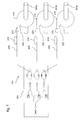
- FIGS. 5A to 5D refer to embodiments of a spatial filter element 136.
- the radiation of higher waveguide modes is effected by a single curvature in the strip waveguide 136a.
- the strip waveguide 136b comprises a strongly curved waveguide section with two opposing curvatures.
- the waveguide section forms, for example, a semicircle.
- Such a double-curved waveguide section suppresses the guidance of higher modes.
- FIG. 5C refers to an embodiment in which a strip waveguide 136c has a portion with a constriction 136d.
- the course of the narrowing follows a mathematical function, which allows the basic mode to pass almost unattenuated.
- the FIG. 5D refers to a spatial filter element 136 having a multimode interference (MMI) region 136g and different conductor widths for the input-side strip waveguide 136e and the output-side strip waveguide 136f.
- MMI multimode interference
- the integrated optical circuit has exactly one of the optical modules 101 comprising a directional coupling element 130, a phase modulator unit 150 and a decoupling element 160.
- An integrated optical circuit with precisely such an optical module 101 is suitable, for example, for measuring direct current or alternating current in exactly one conductor.
- the integrated optical circuit 100 comprises exactly three or more, in principle, identical optical modules.
- Each optical module comprises a directional coupling element, for example comprising a waveguide combining element 132, a polarization element 134, a spatial filter element 136 and a waveguide branch element 138, and a phase modulator unit, for example with a first, a first strip waveguide 141 and a second waveguide coupling element 160 for coupling the first and second strip waveguides 141, 142 to an optical fiber line 202.
- Each output port of the optical modules 101 is a detector element 120a, 120b, 120c assigned, which is optically coupled to the respective output port.
- the input ports of the three optical modules are coupled to the same light source 110, for example via a 1: 3 waveguide branch element 114/116.
- an additional polarization element 112 is provided between the light source 110 and the 1: 3 waveguide branch element 114/116.
- the 1: 3 waveguide branching element 114/116 consists, for example, of a first beam splitter 114, which splits an optical input signal in the ratio 67%: 33%, and a second beam splitter 116, which uniformly distributes the 67% output signal of the first beam splitter 114 distributed on the two output-side strip waveguide.
- the light source 110 and the detector elements 120a, 120b, 120c can either be monolithically integrated on the same substrate on which the optical modules are integrated. According to another embodiment, they are processed on separate chips and optically coupled to the optical module 101.
- FIG. 7 shows an embodiment of a measuring device 901, for measuring in a three-phase system with three current-carrying conductors 900a, 900b, 900c by means of the integrated optical circuit 100 of FIG. 6 ,
- the structure is analogous to that in the FIG. 1B shown construction.
- Each of the current-carrying conductors 900 a, 900 b, 900 c is associated with one of the optical modules of the optical circuit 100.
- the FIG. 8 refers to another embodiment of an integrated optical circuit having three substantially similar optical modules for measuring currents in three-phase systems.
- the embodiment is based on a 1: 3 divider 113, which distributes the signal of the light source 110 to the three input ports of the three optical modules.
- All strip waveguides are, for example, nanowave conductors in which only one of the two linearly polarized eigenmodes is capable of propagation, so that integrated-optical polarizers can be dispensed with.
- Each of the optical modules comprises a 2: 2 directional coupler 139a, 139b, 139c, each having an optical signal at a first port of a first pair of ports on a first and second port of a second pair of ports and optical signals at the gates of the second pair of ports on the second goal of the first Torzies leads.
- the power divider can be designed as an MMI coupler (multimode interference coupler). The embodiment avoids waveguide crossings.
- the light source 110 and the detector elements 120a, 120b, 120c can either be monolithically integrated or manufactured separately and optically coupled to the optical modules.
- the integrated optical circuit 100 is thermally coupled to a thermoelectric element that is controlled so that the integrated optical circuit can operate with a deviation from the operating temperature of less than 0.1 ° C.
- the FIG. 9 relates to a method of measuring current based on the Faraday effect by means of an integrated optical circuit.
- a first and a second optical polarized signal are transmitted via a first and a second strip waveguide, respectively, to a waveguide coupling element (902).
- the first and the second optical signal are coupled to an optical fiber line of a measuring head (904), wherein the optical signal transmitted via the second strip waveguide is coupled to a different polarization mode of the optical fiber line than the first optical signal.
- the optical signal reflected by the measuring head contains two partial optical signals of different polarization.
- the first partial optical signal is coupled to the waveguide coupling element in the first strip waveguide and the second partial optical signal in the second strip waveguide (906), wherein the polarization is reciprocally rotated.
- the two optical partial signals obtained in the two strip waveguides from the reflected signal have the same polarization and have a phase shift relative to one another which corresponds to the strength of a magnetic field to which the measuring head is exposed.
- the phase difference is detected (908) and closed back to the current from the phase difference.
- the phase difference between the first and second optical signals is regulated to a predetermined value by means of a phase modulator.
Landscapes
- Engineering & Computer Science (AREA)
- Power Engineering (AREA)
- Physics & Mathematics (AREA)
- General Physics & Mathematics (AREA)
- Optical Modulation, Optical Deflection, Nonlinear Optics, Optical Demodulation, Optical Logic Elements (AREA)
- Optical Integrated Circuits (AREA)
- Measuring Instrument Details And Bridges, And Automatic Balancing Devices (AREA)
Applications Claiming Priority (1)
| Application Number | Priority Date | Filing Date | Title |
|---|---|---|---|
| DE102012002984A DE102012002984A1 (de) | 2012-02-15 | 2012-02-15 | Integrierter optischer Schaltkreis und Verfahren zur Strommessung sowie Sensormodul und Messeinrichtung |
Publications (2)
| Publication Number | Publication Date |
|---|---|
| EP2629102A2 true EP2629102A2 (fr) | 2013-08-21 |
| EP2629102A3 EP2629102A3 (fr) | 2017-11-22 |
Family
ID=47598660
Family Applications (1)
| Application Number | Title | Priority Date | Filing Date |
|---|---|---|---|
| EP13000143.1A Withdrawn EP2629102A3 (fr) | 2012-02-15 | 2013-01-11 | Circuit optique intégré et procédé de mesure de courant ainsi que module de capteur et dispositif de mesure |
Country Status (3)
| Country | Link |
|---|---|
| US (1) | US9417267B2 (fr) |
| EP (1) | EP2629102A3 (fr) |
| DE (1) | DE102012002984A1 (fr) |
Cited By (3)
| Publication number | Priority date | Publication date | Assignee | Title |
|---|---|---|---|---|
| WO2017190063A3 (fr) * | 2016-04-28 | 2018-02-15 | General Electric Company | Circuits intégrés photoniques et dispositifs de détection photonique |
| WO2018040261A1 (fr) * | 2016-08-30 | 2018-03-08 | Huawei Technologies Co., Ltd. | Procédé et appareil d'obtention de mesures optiques dans un dispositif traitant des signaux optiques à faisceau divisé |
| CN108369250A (zh) * | 2015-10-14 | 2018-08-03 | Abb瑞士股份有限公司 | 具有对连接器未对准的容差的光导纤维电流传感器 |
Families Citing this family (10)
| Publication number | Priority date | Publication date | Assignee | Title |
|---|---|---|---|---|
| CN106030318B (zh) * | 2013-12-20 | 2020-11-17 | Abb电网瑞士股份公司 | 光纤传感器和方法 |
| US9618743B2 (en) | 2015-03-26 | 2017-04-11 | Canon Kabushiki Kaisha | Adaptive optics system with polarization sensitive spatial light modulators |
| JP6769818B2 (ja) * | 2016-10-07 | 2020-10-14 | 日本放送協会 | アンテナ特性測定装置 |
| JP6769817B2 (ja) * | 2016-10-07 | 2020-10-14 | 日本放送協会 | アンテナ特性測定装置 |
| EP3776032A1 (fr) * | 2018-04-12 | 2021-02-17 | ABB Power Grids Switzerland AG | Fibre optique épissée avec protection d'épissure, capteur de courant avec une telle fibre optique épissée et procédé de protection d'une fibre optique épissée |
| US11473191B2 (en) * | 2019-02-27 | 2022-10-18 | Applied Materials, Inc. | Method for creating a dielectric filled nanostructured silica substrate for flat optical devices |
| DE102020132700A1 (de) * | 2020-12-08 | 2022-06-09 | Trumpf Laser- Und Systemtechnik Gmbh | Hochenergieglasschneiden |
| EP4050347A1 (fr) * | 2021-02-25 | 2022-08-31 | Siemens Aktiengesellschaft | Procédé de surveillance d'au moins un élément à semi-conducteur dans un module de semi-conducteur |
| US11609392B1 (en) * | 2022-02-24 | 2023-03-21 | X Development Llc | Photonic coupler |
| CN117930446A (zh) * | 2024-03-25 | 2024-04-26 | 北京航空航天大学 | 一种传感用片上集成光收发组件及其工作方法 |
Family Cites Families (12)
| Publication number | Priority date | Publication date | Assignee | Title |
|---|---|---|---|---|
| DE3801272A1 (de) * | 1988-01-19 | 1989-07-27 | Andreas Dr Neyer | Integriert-optische polarisationsweiche fuer monomode-uebertragungssysteme und ihre verwendung |
| US5235658A (en) * | 1992-03-30 | 1993-08-10 | At&T Bell Laboratories | Method and apparatus for connecting an optical fiber to a strip waveguide |
| DE4216152A1 (de) * | 1992-05-15 | 1993-11-18 | Asea Brown Boveri | Faseroptischer Sensor |
| JP3870420B2 (ja) * | 1995-12-26 | 2007-01-17 | セイコーエプソン株式会社 | アクティブマトリクス基板の製造方法、エレクトロルミネッセンス装置の製造方法、表示装置の製造方法、及び電子機器の製造方法 |
| DE10021669A1 (de) * | 2000-05-05 | 2001-11-08 | Abb Research Ltd | Faseroptischer Stromsensor |
| EP1174719A1 (fr) * | 2000-07-10 | 2002-01-23 | Abb Research Ltd. | Capteur de courant à fibre optique |
| JP2003195239A (ja) * | 2001-12-25 | 2003-07-09 | Nec Corp | 集積型光導波路デバイス |
| US7554347B2 (en) * | 2002-03-19 | 2009-06-30 | Georgia Tech Research Corporation | High input/output density optoelectronic probe card for wafer-level test of electrical and optical interconnect components, methods of fabrication, and methods of use |
| US7378861B1 (en) * | 2003-04-07 | 2008-05-27 | Luxtera, Inc. | Optical alignment loops for the wafer-level testing of optical and optoelectronic chips |
| US20070222460A1 (en) * | 2006-03-07 | 2007-09-27 | Price Joseph K | Mobile apparatus capable of surface measurements |
| US7257283B1 (en) * | 2006-06-30 | 2007-08-14 | Intel Corporation | Transmitter-receiver with integrated modulator array and hybrid bonded multi-wavelength laser array |
| WO2010137752A1 (fr) * | 2009-05-25 | 2010-12-02 | 부산대학교 산학협력단 | Capteur de courant à guide d'onde optique polymère |
-
2012
- 2012-02-15 DE DE102012002984A patent/DE102012002984A1/de not_active Ceased
-
2013
- 2013-01-11 EP EP13000143.1A patent/EP2629102A3/fr not_active Withdrawn
- 2013-02-08 US US13/815,204 patent/US9417267B2/en not_active Expired - Fee Related
Non-Patent Citations (1)
| Title |
|---|
| None * |
Cited By (5)
| Publication number | Priority date | Publication date | Assignee | Title |
|---|---|---|---|---|
| CN108369250A (zh) * | 2015-10-14 | 2018-08-03 | Abb瑞士股份有限公司 | 具有对连接器未对准的容差的光导纤维电流传感器 |
| US10877076B2 (en) | 2015-10-14 | 2020-12-29 | Abb Power Grids Switzerland Ag | Fiber-optic current sensor with tolerance to connector misalignment |
| WO2017190063A3 (fr) * | 2016-04-28 | 2018-02-15 | General Electric Company | Circuits intégrés photoniques et dispositifs de détection photonique |
| WO2018040261A1 (fr) * | 2016-08-30 | 2018-03-08 | Huawei Technologies Co., Ltd. | Procédé et appareil d'obtention de mesures optiques dans un dispositif traitant des signaux optiques à faisceau divisé |
| US10386582B2 (en) | 2016-08-30 | 2019-08-20 | Huawei Technoogies Co., Ltd. | Method and apparatus for obtaining optical measurements at an optical coupler having two inputs and two outputs |
Also Published As
| Publication number | Publication date |
|---|---|
| DE102012002984A1 (de) | 2013-08-22 |
| US20130234698A1 (en) | 2013-09-12 |
| US9417267B2 (en) | 2016-08-16 |
| EP2629102A3 (fr) | 2017-11-22 |
Similar Documents
| Publication | Publication Date | Title |
|---|---|---|
| EP2629102A2 (fr) | Circuit optique intégré et procédé de mesure de courant ainsi que module de capteur et dispositif de mesure | |
| DE69801375T2 (de) | Integrierte optische schaltung | |
| DE3609507C2 (de) | Faseroptisches Interferometer | |
| EP1154278B1 (fr) | Capteur de courant à fibre optique | |
| DE68905757T2 (de) | Integrierte optikvorrichtung zur messung des brechungsindex einer fluessigkeit. | |
| DE69113909T2 (de) | Optischer verzweigender Wellenleiter. | |
| DE3687272T2 (de) | Optischer leistungsteiler und polarisationsteiler. | |
| DE69431513T2 (de) | Fühler für elektrische felder | |
| DE69409099T2 (de) | Steuerung von spektralverschiebungsfehlern | |
| EP1299736A1 (fr) | Capteur de courant a fibre optique | |
| DE69713375T2 (de) | Integrierter interferometer | |
| DE69414808T2 (de) | Optischer Wellenleiter mit schräger Endfläche | |
| WO2004029544A1 (fr) | Dispositif de mesure interferometrique | |
| DE69115877T2 (de) | Gerät zum messen der winkelgeschwindigkeit durch optische interferenz | |
| DE202018006722U1 (de) | Abstandsmessanordnung zur Bestimmung eines Abstandes zu einem Objekt | |
| DE69030810T2 (de) | Pockelseffekt-Messsonde für elektrische Felder | |
| DE102011104512A1 (de) | Lichtquellen- und Kopplermodul für ein mehrstufiges Sensorsystem | |
| DE102009013878B3 (de) | Sensoranordnung und Detektionsverfahren | |
| DE60118662T2 (de) | Anordnung zum Messen des elektrischen Stromes durch den Faraday-Effekt | |
| DE102016202210B4 (de) | Laseranordnung, Verfahren zum Steuern eines Lasers und Messverfahren | |
| DE4308411A1 (de) | Interferometer in integriert-optischer Bauweise | |
| EP1368667B1 (fr) | Procede et dispositif de mesure de courant au moyen d'un interferometre de sagnac en ligne a fibres optiques et modulateur de phase approprie | |
| WO2015024915A1 (fr) | Module de détection | |
| WO2003042708A2 (fr) | Detecteur de courant a fibres optiques, comportant plusieurs tetes de detection | |
| DE3920840C1 (en) | Integrated optical sensor detecting temp. and refraction index changes - has double refractive waveguide in substrate extending along X or Y axis of cut lithium-niobate crystal |
Legal Events
| Date | Code | Title | Description |
|---|---|---|---|
| PUAI | Public reference made under article 153(3) epc to a published international application that has entered the european phase |
Free format text: ORIGINAL CODE: 0009012 |
|
| AK | Designated contracting states |
Kind code of ref document: A2 Designated state(s): AL AT BE BG CH CY CZ DE DK EE ES FI FR GB GR HR HU IE IS IT LI LT LU LV MC MK MT NL NO PL PT RO RS SE SI SK SM TR |
|
| AX | Request for extension of the european patent |
Extension state: BA ME |
|
| PUAL | Search report despatched |
Free format text: ORIGINAL CODE: 0009013 |
|
| AK | Designated contracting states |
Kind code of ref document: A3 Designated state(s): AL AT BE BG CH CY CZ DE DK EE ES FI FR GB GR HR HU IE IS IT LI LT LU LV MC MK MT NL NO PL PT RO RS SE SI SK SM TR |
|
| AX | Request for extension of the european patent |
Extension state: BA ME |
|
| RIC1 | Information provided on ipc code assigned before grant |
Ipc: G01R 15/24 20060101AFI20171013BHEP |
|
| STAA | Information on the status of an ep patent application or granted ep patent |
Free format text: STATUS: REQUEST FOR EXAMINATION WAS MADE |
|
| 17P | Request for examination filed |
Effective date: 20180413 |
|
| RBV | Designated contracting states (corrected) |
Designated state(s): AL AT BE BG CH CY CZ DE DK EE ES FI FR GB GR HR HU IE IS IT LI LT LU LV MC MK MT NL NO PL PT RO RS SE SI SK SM TR |
|
| GRAP | Despatch of communication of intention to grant a patent |
Free format text: ORIGINAL CODE: EPIDOSNIGR1 |
|
| STAA | Information on the status of an ep patent application or granted ep patent |
Free format text: STATUS: GRANT OF PATENT IS INTENDED |
|
| INTG | Intention to grant announced |
Effective date: 20201202 |
|
| STAA | Information on the status of an ep patent application or granted ep patent |
Free format text: STATUS: THE APPLICATION IS DEEMED TO BE WITHDRAWN |
|
| 18D | Application deemed to be withdrawn |
Effective date: 20210413 |