EP2629105B1 - Procédé pour effectuer une comparaison à trois états de deux signaux d'entrée et circuit comparateur à fenêtre - Google Patents
Procédé pour effectuer une comparaison à trois états de deux signaux d'entrée et circuit comparateur à fenêtre Download PDFInfo
- Publication number
- EP2629105B1 EP2629105B1 EP13150753.5A EP13150753A EP2629105B1 EP 2629105 B1 EP2629105 B1 EP 2629105B1 EP 13150753 A EP13150753 A EP 13150753A EP 2629105 B1 EP2629105 B1 EP 2629105B1
- Authority
- EP
- European Patent Office
- Prior art keywords
- voltage
- offset
- capacitor
- input
- series
- Prior art date
- Legal status (The legal status is an assumption and is not a legal conclusion. Google has not performed a legal analysis and makes no representation as to the accuracy of the status listed.)
- Active
Links
Images


Classifications
-
- G—PHYSICS
- G01—MEASURING; TESTING
- G01R—MEASURING ELECTRIC VARIABLES; MEASURING MAGNETIC VARIABLES
- G01R19/00—Arrangements for measuring currents or voltages or for indicating presence or sign thereof
- G01R19/165—Indicating that current or voltage is either above or below a predetermined value or within or outside a predetermined range of values
- G01R19/16566—Circuits and arrangements for comparing voltage or current with one or several thresholds and for indicating the result not covered by subgroups G01R19/16504, G01R19/16528, G01R19/16533
- G01R19/1659—Circuits and arrangements for comparing voltage or current with one or several thresholds and for indicating the result not covered by subgroups G01R19/16504, G01R19/16528, G01R19/16533 to indicate that the value is within or outside a predetermined range of values (window)
-
- G—PHYSICS
- G06—COMPUTING OR CALCULATING; COUNTING
- G06F—ELECTRIC DIGITAL DATA PROCESSING
- G06F3/00—Input arrangements for transferring data to be processed into a form capable of being handled by the computer; Output arrangements for transferring data from processing unit to output unit, e.g. interface arrangements
- G06F3/01—Input arrangements or combined input and output arrangements for interaction between user and computer
- G06F3/03—Arrangements for converting the position or the displacement of a member into a coded form
- G06F3/0304—Detection arrangements using opto-electronic means
- G06F3/0317—Detection arrangements using opto-electronic means in co-operation with a patterned surface, e.g. absolute position or relative movement detection for an optical mouse or pen positioned with respect to a coded surface
-
- G—PHYSICS
- G06—COMPUTING OR CALCULATING; COUNTING
- G06F—ELECTRIC DIGITAL DATA PROCESSING
- G06F3/00—Input arrangements for transferring data to be processed into a form capable of being handled by the computer; Output arrangements for transferring data from processing unit to output unit, e.g. interface arrangements
- G06F3/01—Input arrangements or combined input and output arrangements for interaction between user and computer
- G06F3/03—Arrangements for converting the position or the displacement of a member into a coded form
- G06F3/033—Pointing devices displaced or positioned by the user, e.g. mice, trackballs, pens or joysticks; Accessories therefor
- G06F3/0354—Pointing devices displaced or positioned by the user, e.g. mice, trackballs, pens or joysticks; Accessories therefor with detection of two-dimensional [2D] relative movements between the device, or an operating part thereof, and a plane or surface, e.g. 2D mice, trackballs, pens or pucks
- G06F3/03543—Mice or pucks
-
- G—PHYSICS
- G06—COMPUTING OR CALCULATING; COUNTING
- G06F—ELECTRIC DIGITAL DATA PROCESSING
- G06F3/00—Input arrangements for transferring data to be processed into a form capable of being handled by the computer; Output arrangements for transferring data from processing unit to output unit, e.g. interface arrangements
- G06F3/01—Input arrangements or combined input and output arrangements for interaction between user and computer
- G06F3/03—Arrangements for converting the position or the displacement of a member into a coded form
- G06F3/033—Pointing devices displaced or positioned by the user, e.g. mice, trackballs, pens or joysticks; Accessories therefor
- G06F3/038—Control and interface arrangements therefor, e.g. drivers or device-embedded control circuitry
- G06F3/0383—Signal control means within the pointing device
-
- H—ELECTRICITY
- H03—ELECTRONIC CIRCUITRY
- H03K—PULSE TECHNIQUE
- H03K5/00—Manipulating of pulses not covered by one of the other main groups of this subclass
- H03K5/22—Circuits having more than one input and one output for comparing pulses or pulse trains with each other according to input signal characteristics, e.g. slope, integral
- H03K5/24—Circuits having more than one input and one output for comparing pulses or pulse trains with each other according to input signal characteristics, e.g. slope, integral the characteristic being amplitude
-
- G—PHYSICS
- G01—MEASURING; TESTING
- G01R—MEASURING ELECTRIC VARIABLES; MEASURING MAGNETIC VARIABLES
- G01R19/00—Arrangements for measuring currents or voltages or for indicating presence or sign thereof
- G01R19/165—Indicating that current or voltage is either above or below a predetermined value or within or outside a predetermined range of values
- G01R19/16566—Circuits and arrangements for comparing voltage or current with one or several thresholds and for indicating the result not covered by subgroups G01R19/16504, G01R19/16528, G01R19/16533
- G01R19/1659—Circuits and arrangements for comparing voltage or current with one or several thresholds and for indicating the result not covered by subgroups G01R19/16504, G01R19/16528, G01R19/16533 to indicate that the value is within or outside a predetermined range of values (window)
- G01R19/16595—Circuits and arrangements for comparing voltage or current with one or several thresholds and for indicating the result not covered by subgroups G01R19/16504, G01R19/16528, G01R19/16533 to indicate that the value is within or outside a predetermined range of values (window) with multi level indication
Definitions
- the present invention relates to a method for performing a tri-state comparison of two input signals in a window comparator circuit.
- said method can be applied for processing motion of a light detection circuit of an optical pointing device.
- the present invention concerns also the window comparator circuit for implementing the method for performing a tri-state comparison of two input signals.
- Said input signals can be signals from a pixel array, which picks up light reflected on a work surface.
- the light reflected on the work surface has to be picked up by a pixel or photo-detector array in order to be processed in a motion detection processing circuit.
- a comparator array is placed between the pixel or photo-detector array and the motion detection processing circuit.
- Said comparator array is composed of several comparator units to compare successively several signals from the pixel or photo-detector array.
- a window comparator circuit is used for tri-state detection levels. It is to be noted that a tri-state refers to three output states, for example one output state below a lower window voltage, one output state inside some window voltage limits, and one output state above an upper window voltage. For that it is generally not possible to conceive said window comparator circuit only with a simple comparator as usually in the light detection devices of the prior art.
- Said window comparator circuit is composed of two comparators at the output of said circuit.
- Said window comparator circuit allows equalizing hysteresis characteristics of a dead zone width in the upper end and the lower end of said dead zone.
- an operational amplifier combined with a voltage setting unit, a reference voltage source and a power source. Two signals from the voltage setting unit are respectively compared to a reference voltage in the two corresponding comparators.
- said window comparator circuit is made with too many electronic components, which is a drawback. Furthermore it is difficult to match accurately the two comparators to well define a tri-state comparison function, which is another drawback.
- the comparator includes a first capacitor to store a first input signal, a second capacitor to store a ground voltage or a reference voltage, a third capacitor to store a reference voltage or a ground voltage, and a fourth capacitor to store a second input signal.
- a comparator circuit is adapted to compare the first and second input signals. However it is not adapted to be easily used in a comparator array and for any residual offsets to be minimized, which is a drawback.
- the invention therefore concerns a method for performing a tri-state comparison of two input signals in a window comparator circuit, which includes the features defined in the independent claim 1.
- One advantage of the method for performing a tri-state comparison of two input signals in a window comparator circuit of the present invention lies in the fact that a single output comparator is used two times successively in the window comparator circuit. This allows any residual offsets to be minimized and to save die array with a minimum number of electronic components to perform said tri-state comparison. Furthermore said method for performing the tri-state comparison in the window comparator circuit allows for a symmetrical window around a differential voltage at 0 V.
- a different offset voltage can be provided at the input of said window comparator circuit, or by adapting the capacitive ratio of capacitors on which are respectively stored each input voltage signal and offset voltage signal before comparing successively two adapted signals in an output comparator. Only one reference voltage can be used for defining the window function of said window comparator circuit. Said method easily fits into one phase of a two phase autozeroing comparator circuit.
- Another object of the present invention concerns a window comparator circuit for implementing the method for performing a tri-state comparison of two input signals, which includes the features defined in the independent claim 6.
- window comparator circuit Some particular embodiments of the window comparator circuit are defined in the dependent claims 7 to 10.
- window comparator circuit for implementing a method for performing a tri-state comparison between two input signals, in particular for an optical pointing device, such as a computer mouse.
- window comparator circuit can be used also in other technical fields.
- Figure 1 shows a simplified view of a window comparator circuit 1 for implementing a method for performing a tri-state comparison between two input signals V INN and V INP .
- said window comparator circuit 1 can be used in an optical computer mouse as explained hereafter briefly in reference to Figure 4 .
- several window comparator circuits 1 compose a comparator array of said optical computer mouse, where each window comparator circuit 1 is controlled by a motion detection processing circuit in order to compare two input signals V INN and V INP providing successively from a photo-detector array.
- a conventional signal comparator which existed in previous computer mouse, is used for the conception of one part of the window comparator circuit 1 of the present invention.
- this window comparator circuit is controlled for performing a comparison between two input signals V INN and V INP in time in order to implement a window function, and to generate three output levels at the output of said window comparator circuit.
- Said two input signals V INN and V INP have to be compared to determine if the first input signal V INN is less or greater than the second input signal V INP by more than X Volts, where X can be programmed as an offset voltage. So the window is defined as the inner region, where the first input signal V INN is within ⁇ X Volts of the second input signal V INP .
- the window voltage levels are simply capacitively added to one signal or the other signal prior to comparing said two adapted input signals.
- An adapted offset voltage signal is proportionally added to the second adapted input signal V INP in a first phase and to the first adapted input signal V INN in a second successive phase.
- the first adapted input signal which is a first adapted input voltage V INN
- the second adapted input signal which is a second adapted input voltage V INP
- it can be compared for example the second adapted input voltage V INP added to the adapted offset voltage less than the first adapted input voltage V INN .
- the adaptation of each signal depends on a capacitive ratio as explained hereafter.
- the window comparator circuit 1 to implement the method for performing a tri-state comparison of the two input signals is now explained in more details in reference to Figures 1 to 3 .
- Said window comparator circuit 1 includes a first series of switches SW1, SW2, SW3, SW4, a second series of switches SW11, SW12, SW13, SW14, a third series of switches SW21, SW22, SW23, SW24, four capacitors C 1n , C 2n , C 1p , C 2p and a single comparator 2.
- Each switch can be made with a transistor MOS, and for example with a NMOS transistor with the gate control by a specific control signal in order to open said switch through the connection of source and drain terminals, with a high voltage as a regulated voltage supplied to the gate terminal, and to close said switch with a ground voltage supplied to the gate terminal.
- Said capacitors can be made also with some MOS transistors, for example with PMOS transistors.
- said PMOS transistors have each source and drain terminals, and the n-well terminal connected to a high potential terminal of a power supply source or to a regulated voltage, whereas a gate terminal is used as the negative terminal of each capacitor. So said PMOS transistors are mounted in an inversion mode to make said capacitors, which is preferable to an accumulation mode.
- each NMOS transistor has source and drain terminals, and the p-well or bulk terminal connected to a ground voltage, whereas a gate terminal is used as the positive terminal of the capacitor as shown on Figure 1 .
- First and fourth switches SW1, SW4 of the first series of switches receive at the input an offset determined voltage Offset, whereas second and third switches SW2, SW3 receive at the input a ground voltage.
- the first and third switches SW1, SW3 of the first series of switches are controlled by a negative offset control signal ONb, whereas the second and fourth switches SW2, SW4 of the first series of switches are controlled by a positive offset control signal ON, which is the reverse of the negative offset control signal ONb.
- the positive offset control signal ONb When the negative offset control signal ONb is in a "0" state, the positive offset control signal ON is in a "1" state in a first phase of the method. So in this first phase of the method, the ground voltage passes through the second closed switch SW2 of the first series of switches, whereas the offset voltage Offset passes through the fourth closed switch SW4 of the first series of switches. In the first phase, the first switch SW1 and the third switch SW3 are in an open state. When the negative offset control signal ONb is in a "1" state, the positive offset control signal ON is in a "0" state in a second phase of the method.
- the offset voltage Offset passes through the first closed switch SW1 of the first series of switches, whereas the ground voltage passes through the third closed switch SW3 of the first series of switches.
- the second switch SW2 and the fourth switch SW4 are in an open state.
- the four switches SW11, SW12, SW13, SW14 of the second series of switches are each controlled by a same first control signal Z.
- Said first control signal Z has a frequency two times greater than the frequency of each offset control signal ON, ONb.
- Said second series of switches includes a first switch SW11 to receive at the input the first input signal V INN , which is preferably a first input voltage V INN providing for example from one selected pixel of the pixel or photo-detector array.
- V INN a first input voltage V INN providing for example from one selected pixel of the pixel or photo-detector array.
- a second switch SW12 of the second series of switches receives at the input in the first phase, the ground voltage, and in the second phase, the offset voltage Offset.
- the first control signal Z is in the "1" state, the ground voltage in the first phase or the offset voltage Offset in the second phase is stored or charged on a second capacitor C 2n .
- a third switch SW13 of the second series of switches receives at the input in the first phase, the offset voltage Offset, and in the second phase, the ground voltage.
- the offset voltage Offset in the first phase or the ground voltage in the second phase is stored or charged on a third capacitor C 2p .
- a fourth switch SW14 of the second series of switches receives at the input the second input voltage V INP providing for example from another selected pixel of the pixel or photo-detector array.
- said second input voltage V INP is stored or charged on a fourth capacitor C 1p .
- the four switches SW21, SW22, SW23, SW24 of the third series of switches are each controlled by a same second control signal C.
- Said second control signal C has the same frequency like the first control signal Z, but the second control signal C is the reverse of the second control signal Z.
- the first switch SW21 of the third series of switches is connected between the first capacitor C 1n and a negative input of a comparator 2.
- the second switch SW22 of the third series of switches is connected between the second capacitor C 2n and the negative input of the comparator 2.
- the third switch SW23 of the third series of switches is connected between the third capacitor C 2p and the positive input of the comparator 2.
- the fourth switch SW23 of the third series of switches is connected between the fourth capacitor C 1p and the positive input of the comparator 2.
- the first signal control Z When the second control signal C is in a "1" state, the first signal control Z is in a "0" state, and when the second control signal C is in a "0" state, the first signal control Z is in a "1" state.
- the change of state of the second control signal C occurs with a slight delay after the change of state of the first control signal Z in order to perform a well defined comparison in the comparator 2.
- the second control signal C in a "1" state With the second control signal C in a "1” state, the first capacitor C 1n and the second capacitor C 2n are connected in parallel to the negative input of the comparator 2, and the third capacitor C 2p and the fourth capacitor C 1p are connected in parallel to the positive input of the comparator 2.
- the first adapted voltage V xn at the negative input of the comparator 2 corresponds to the first input voltage, which is capacitively adapted by the factor N/(N+M).
- the second adapted voltage V xp corresponds to the second input voltage, which is capacitively adapted by the factor N'/(N'+M'), added to the offset voltage, which is capacitively adapted by the factor M'/(N'+M').
- the first adapted voltage V xn at the negative input of the comparator 2 corresponds to the first input voltage V INN , which is capacitively adapted by the factor N/(N+M), added to the offset voltage, which is capacitively adapted by the factor M/(N+M).
- the second adapted voltage at the positive input of the comparator 2 corresponds to the second input voltage V INP , which is capacitively adapted by the factor N'/(N'+M').
- the capacitive value of the first capacitor C 1n corresponds to the capacitive value of the fourth capacitor C 1p
- the capacitive value of the second capacitor C 2n corresponds to the capacitive value of the third capacitor C 2p
- the capacitive factor N/(N+M) corresponds to the capacitive factor N'/(N'+M')
- the capacitive factor M/(N+M) corresponds to the capacitive factor M'/(N'+M').
- the second and third capacitors C 2n and C 2p can be each considered as a unit capacitor made for example with a PMOS transistor, which is connected in a preferred inversion mode or in an accumulation mode.
- the first and fourth capacitors C 1n and C 1p can be made each with 9 unit capacitors, to have a capacitive value corresponding to 9 times the capacitive value of the second or third capacitors C 2n and C 2p . With these capacitive values, said capacitors can be easily matched in an integrated circuit.
- the four capacitors C 1n , C 2n , C 2p , C 1p can be configured as 20 unit capacitors placed under a rectangular shape with seven unit capacitors for the length and three unit capacitors for the width.
- the offset voltage Offset is multiplied by the factor 1/10 to be added to the second or first input voltage V INP or V INN , which is multiplied by the factor 9/10, in the first or second phase of the method.
- the adapted offset voltage for the first and second phases of the method it is defined a tri-state comparison in the window comparator circuit 1.
- a first output signal OUT 1 is provided at the output of the comparator 2, which is stored for example in memory by means of a processing circuit.
- a second output signal OUT 2 is provided at the output of the comparator 2. If the first input voltage V INN is greater than the second input voltage V INP by more than X Volts, the output signals OUT 1 and OUT 2 are at a "0" state, i.e. at 0 V. If the second input voltage V INP is greater than the first input voltage V INN by more than X Volts, the output signals OUT 1 and OUT 2 are at a "1" state, i.e. at a high level near to a regulated voltage.
- the motion detection processing circuit can easily consider the three levels of said window comparator circuit 1 in order to improve the detection of the motion of the computer mouse on a work surface.
- the X value corresponds to (M/N) ⁇ Offset supplied at the input of said window comparator circuit 1.
- Said offset voltage Offset can be programmed via a 4-bit bus from the processing circuit between 0 and 200 mV or preferably between 0 and 75 mV with an LSB value of 5 mV. in this case, with a maximum offset voltage at 75 mV, the first input voltage V INN has to be greater or lower, than the second input voltage V INP by more or less than approximately 8.5 mV to obtain the two output signals OUT 1 and OUT 2 at a low level or a high level.
- the voltage range of each input voltage is between 0 and 500 mV and often close to 50 mV or 100 mV depending on the light reflected on a work surface and picked up by the pixels of the photo-detector array.
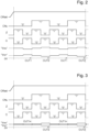
- Figure 2 schematically shows a temporal diagram of some signals through the window comparator circuit, in which a first input voltage V INN is sufficiently greater than a second input voltage V INP by more than (M/N) ⁇ Offset.
- the negative offset control signal ONb in a first phase of the method, is in a "0" state, whereas in a second phase of the method, the negative signal ONb is a "1" state.
- the positive offset control signal ON not shown is exactly the reverse of the negative offset control signal ONb.
- the duration for each state of said negative offset control signal ONb can be defined close to 2.5 ⁇ s for a frequency of said negative control signal ONb at 200 kHz.
- the first control signal Z and the second control signal C which is the reverse of the first control signal Z, have duration of each state corresponding to the half of the duration of the negative offset control signal, at 1.25 ⁇ s. If the frequency of the negative control signal ONb is at 200 kHz, the frequency of the first and second control signals Z and C is at 400 kHz. It can be envisaged to reduce said duration of each state for the first control signal Z and the second control signal C until a minimum of 500 ns.
- the first output signal OUT 1 and the second output signal OUT 2 are each at 0 V.
- the first phase of the method and when the second control signal C in a "1" state that the first adapted voltage based on the first input voltage V INN is slightly reduced, whereas the second adapted voltage based on the second input voltage V INP is slightly increased, but lower than the first adapted signal.
- the first adapted voltage is slightly increased, whereas the second adapted voltage is slightly reduced. So the two output signals OUT 1 and OUT 2 are effectively at 0 V to define the first level of the window comparator circuit.
- the two output signals OUT 1 and OUT 2 are in this case at a high level in the "1" state. So this defines the third level of the window comparator circuit, but not shown in Figures 2 and 3 .
- Figure 3 schematically shows a temporal diagram of some signals through the window comparator circuit, in which a first input voltage V INN is within ⁇ (MZN) ⁇ Offset with respect to the second input voltage V INP . in this case, a second or intermediate level of the window comparator circuit is shown.
- the second adapted voltage comes higher than the first adapted voltage when the second control signal C is in a "1" state. So the first output signal OUT 1 is at a high level in the "1" state in said first phase.
- the first adapted voltage is higher than the second adapted voltage when the second control signal C is in a "1" state. So the second output signal OUT 2 is at 0 V.
- the processing circuit can interpret the two different output signals OUT 1 and OUT 2 for considering the second or intermediate level of window comparator circuit.
- Figure 4 shows a generalized schematic block diagram of an optical pointing device as defined also in the patent application US 2007/0290121 A1 .
- It generally includes at least one coherent light source 130, such as a laser illumination source, which produces radiation at a determined flash rate on a portion of a work surface S, and a pixel or photo-detector array 100 having a plurality of pixels, to pick up the light reflected on said work surface S.
- a non-coherent light source such as a LED source, so that the method can work with either coherent or non-coherent light.
- This photo-detector array 100 is coupled to processing means 110, such as a motion detection processing circuit, for processing the signals outputted by the photo-detector array 100.
- a comparator array 120 is interposed between processing means 110 and pixel array 100.
- Said comparator array 120 includes a plurality of window comparator circuits each for comparing the light intensity of a first pixel of array 100 with the light intensity of a second pixel of array 100 and for outputting a comparison signal in one of the three states defined by the window comparator circuit of the present invention, and also resulting motion feature conditions.
- the coherent or non-coherent light source 130 of the optical pointing device produces radiation at a determined flash rate, that impinges with a determined gradient on a portion of a work surface S.
- Said work surface S may be a planar or non-planar surface, such as a surface over which the pointing device is moved (as in the case of an optical mouse), the surface of a ball (as in the case of an optical trackball) or any other suitable surface that may provide an appropriate speckled intensity pattern for detection by photo-detector array 100.
- Processing means 110 is further adapted to communicate in a bidirectional manner with an interface 140 that communicates in turn with a host system (not illustrated) over a bus 150. Cursor control signals (and eventually other signals related to the optical pointing device) are supplied to the host system over bus 150. Processing means 110 may also receive information, such as configuration signals, over bus 150 from the host system.
- Processing means 110 is essentially designed to intermittently sample the pixel outputs of photo-detector array 100 in accordance with a defined sequence. The information of two successive samples or speckled images is compared and a relative motion measurement is extracted by processing means 110. The adequate cursor control signals are then derived from the relative motion measurement and transmitted to the host system via line interface 140.
- processing means 110 can be provided with a very simple selecting factor which promotes detection of one type of motion feature rather than the other type.
- the capacitive factor for adaptation of the first or second input voltage and for adaptation of the offset voltage can be programmed to different values preferably between 1/2 and 1/20.
- the first series of switches can be replaced by a multiplexer with two inputs and two outputs and controlled by a 2-bit control signal.
Landscapes
- Engineering & Computer Science (AREA)
- General Engineering & Computer Science (AREA)
- Theoretical Computer Science (AREA)
- Physics & Mathematics (AREA)
- General Physics & Mathematics (AREA)
- Human Computer Interaction (AREA)
- Nonlinear Science (AREA)
- Manipulation Of Pulses (AREA)
Claims (9)
- Procédé pour réaliser une comparaison à trois états de deux signaux d'entrée dans un circuit comparateur à fenêtre (1), caractérisé en ce que le procédé comprend une première phase pour:- stocker la tension d'un premier signal d'entrée (VINN) sur un premier condensateur (C1n), et une tension de masse sur un deuxième condensateur (C2n);- stocker une tension de décalage (Offset) sur un troisième condensateur (C2p), et la tension d'un deuxième signal d'entrée (VINP) sur un quatrième condensateur (C1p);- comparer, dans un comparateur (2), la première tension d'entrée (VINN), qui est adaptée par un premier facteur défini par le rapport N/(N+M), où N est la valeur capacitive du premier condensateur (C1n), et M est la valeur capacitive du deuxième condensateur (C2n), à la deuxième tension d'entrée, qui est adaptée par un deuxième facteur défini par le rapport N'/(N'+M'), où N' est la valeur capacitive du quatrième condensateur (C1p), et M' est la valeur capacitive du troisième condensateur (C2p), et ajoutée à la tension de décalage, qui est adaptée par un troisième facteur défini par M'/(N'+M'), pour fournir un premier signal de sortie (OUT1),et en ce que le procédé comprend une deuxième phase pour :- stocker la tension du premier signal d'entrée (VINN) sur le premier condensateur (C1n), et la tension de décalage (Offset) sur le deuxième condensateur (C2n) ;- stocker la tension de masse sur le troisième condensateur (C2p), et la tension du deuxième signal d'entrée (VINP) sur le quatrième condensateur (C1p) ;- comparer, dans le comparateur (2), la première tension d'entrée, qui est adaptée par le premier facteur défini par le rapport N/(N+M), ajoutée à la tension de décalage (Offset), qui est adaptée par un quatrième facteur défini par le rapport M/(N+M), à la deuxième tension d'entrée, qui est adaptée par le deuxième facteur défini par le rapport N'/(N'+M'), pour fournir un deuxième signal de sortie (OUT2), et- commander l'état des premier et deuxième signaux de sortie pour déterminer si la comparaison des premier et deuxième signaux d'entrée est dans un état bas ou dans un état haut si les premier et deuxième signaux de sortie ont un même niveau de sortie bas ou haut, ou dans un état intermédiaire si les premier et deuxième signaux de sortie ont un niveau de sortie différent.
- Procédé selon la revendication 1, caractérisé en ce que, dans la première phase et la deuxième phase du procédé, le premier facteur pour adapter la première tension d'entrée est égal au deuxième facteur pour adapter la deuxième tension d'entrée, et le troisième facteur pour adapter la tension de décalage (Offset) est égal au quatrième facteur pour adapter la tension de décalage (Offset).
- Procédé selon la revendication 2, caractérisé en ce que, dans les première et deuxième phases du procédé, les première et deuxième tensions d'entrée sont adaptées par les premier et deuxième facteurs, qui sont 9 fois plus grands que les troisième et quatrième facteurs pour adapter la tension de décalage (Offset).
- Procédé selon la revendication 1, pour lequel le circuit comparateur à fenêtre (1) inclut une première série de quatre commutateurs, un premier commutateur (SW1) et un quatrième commutateur (SW4) recevant, à l'entrée, la tension de décalage (Offset), et un deuxième commutateur (SW2) et un troisième commutateur (SW3) recevant, à l'entrée, la tension de masse, les premier et troisième commutateurs étant commandés par un signal de commande de décalage négatif (ONb), tandis que les deuxième et quatrième commutateurs sont commandés par un signal de commande de décalage positif (ON), qui est l'inverse du signal de commande de décalage négatif (ONb),caractérisé en ce que, dans la première phase du procédé, le deuxième commutateur (SW2) et le quatrième commutateur (SW4) sont fermés par le signal de commande de décalage positif (ON) afin de stocker la tension de masse sur le deuxième condensateur (C2n) et la tension de décalage sur le troisième condensateur (C2p), eten ce que, dans la deuxième phase du procédé, le premier commutateur et le troisième commutateur sont fermés par le signal de commande de décalage négatif (ONb) afin de stocker la tension de décalage (Offset) sur le deuxième condensateur (C2n) et la tension de masse sur le troisième condensateur (C2p).
- Procédé selon la revendication 4, pour lequel le circuit comparateur à fenêtre inclut une deuxième série de quatre commutateurs, qui sont chacun commandés par un premier signal de commande (Z), un premier commutateur de la deuxième série recevant, à l'entrée, un premier signal d'entrée (VINN), un deuxième commutateur de la deuxième série recevant la tension de masse dans la première phase du procédé et la tension de décalage (Offset) dans la deuxième phase du procédé, un troisième commutateur de la deuxième série recevant la tension de décalage (Offset) dans la première phase du procédé et la tension de masse dans la deuxième phase du procédé, et un quatrième commutateur de la deuxième série recevant le deuxième signal d'entrée (VINP), pour lequel le circuit comparateur à fenêtre (1) inclut une troisième série de quatre commutateurs, qui sont chacun commandés par un deuxième signal de commande (C), qui est l'inverse du premier signal de commande (Z), un premier commutateur (SW21) de la troisième série étant connecté entre le premier condensateur (C1n) et une première entrée (Vxn) du comparateur (2), un deuxième commutateur (SW22) de la troisième série étant connecté entre le deuxième condensateur (C2n) et la première entrée (Vxn) du comparateur (2), un troisième commutateur (SW23) de la troisième série étant connecté entre le troisième condensateur (C2p) et la deuxième entrée (Vxp) du comparateur (2), et un quatrième commutateur (SW24) de la troisième série étant connecté entre le quatrième condensateur (C1p) et la deuxième entrée (Vxp) du comparateur (2),caractérisé en ce que, dans la première phase du procédé, les commutateurs de la deuxième série de commutateurs sont chacun fermés tout d'abord par le premier signal de commande (C) afin de stocker la première tension d'entrée (VINN) sur le premier condensateur (C1n), la tension de masse sur le deuxième condensateur (C2n), la tension de décalage (Offset) sur le troisième condensateur (C2p) et la deuxième tension d'entrée (VINP) sur le quatrième condensateur (C1p),en ce que, dans la première phase du procédé, les commutateurs de la troisième série de commutateurs sont chacun fermés par le deuxième signal de commande (C), tandis que tous les commutateurs de la deuxième série de commutateurs sont ouverts par le premier signal de commande (Z), afin de comparer la première tension d'entrée (VINN) adaptée par le premier facteur à la deuxième tension d'entrée (VINP) adaptée par le deuxième facteur ajoutée à la tension de décalage adaptée par le troisième facteur,en ce que, dans la deuxième phase du procédé, les commutateurs de la deuxième série de commutateurs sont chacun fermés tout d'abord par le premier signal de commande (Z) afin de stocker la première tension d'entrée (VINN) sur le premier condensateur (C1n), la tension de décalage (Offset) sur le deuxième condensateur (C2n), la tension de masse sur le troisième condensateur (C2p), et la deuxième tension d'entrée (VINP) sur le quatrième condensateur (C1p), eten ce que, dans la deuxième phase du procédé, les commutateurs de la troisième série de commutateurs sont chacun fermés par le deuxième signal de commande (C), tandis que tous les commutateurs de la deuxième série de commutateurs sont ouverts par le premier signal de commande (Z), afin de comparer la première tension d'entrée (VINN) adaptée par le premier facteur ajoutée à la tension de décalage (Offset) adaptée par le quatrième facteur, à la deuxième tension d'entrée adaptée par le deuxième facteur.
- Circuit comparateur à fenêtre (1) configuré pour mettre en oeuvre le procédé pour réaliser une comparaison à trois états de deux signaux d'entrée selon la revendication 5, dans lequel ledit circuit comparateur à fenêtre (1) inclut un premier condensateur (C1n) pour stocker une tension d'un premier signal d'entrée (VINN), un deuxième condensateur (C2n) pour stocker une tension de masse ou une tension de décalage (Offset), un troisième condensateur (C2p) pour stocker la tension de décalage (Offset) ou une tension de masse, et un quatrième condensateur (C1p) pour stocker une tension d'un deuxième signal d'entrée (VINP), et un comparateur (2) pour comparer une première tension d'entrée (VINN) adaptée par un premier facteur défini par le rapport N/(N+M), où N est la valeur capacitive du premier condensateur (C1n), et M est la valeur capacitive du deuxième condensateur (C2n), à une deuxième tension d'entrée (VINP) adaptée par un deuxième facteur défini par le rapport N'/(N'+M'), où N' est la valeur capacitive du quatrième condensateur (C1p), et M' est la valeur capacitive du troisième condensateur (C2p), et ajoutée à la tension de décalage (Offset) adaptée par un troisième facteur défini par M'/(N'+M'), ou pour comparer la première tension d'entrée (VINN) adaptée par le premier facteur ajoutée à la tension de décalage (Offset) adaptée par un quatrième facteur défini par le rapport M/(N+M), à la deuxième tension d'entrée (VINP) adaptée par le deuxième facteur, etledit circuit comparateur à fenêtre (1) inclut une première série de quatre commutateurs, un premier commutateur (SW1) et un quatrième commutateur (SW4) étant destinés à recevoir, à l'entrée, la tension de décalage (Offset), et un deuxième commutateur (SW2) et un troisième commutateur (SW3) étant destinés à recevoir, à l'entrée, la tension de masse, les premier et troisième commutateurs étant commandés par un signal de commande de décalage négatif (ONb), tandis que les deuxième et quatrième commutateurs sont commandés par un signal de commande de décalage positif (ON), qui est l'inverse du signal de commande de décalage négatif (ONb),ledit circuit comparateur à fenêtre (1) inclut une deuxième série de quatre commutateurs, qui sont chacun commandés par un premier signal de commande (Z), un premier commutateur (SW11) de la deuxième série étant destiné à recevoir, à l'entrée, un premier signal d'entrée (VINN) et à stocker, à la sortie, la tension du premier signal d'entrée (VINN) sur le premier condensateur (C1n), un deuxième commutateur (SW12) de la deuxième série étant destiné à recevoir la tension de masse depuis la sortie du deuxième commutateur (SW2) de la première série ou la tension de décalage (Offset) depuis la sortie du premier commutateur (SW1) de la première série afin de stocker, à la sortie, la tension de décalage ou la tension de masse sur le deuxième condensateur (C2n), un troisième commutateur (SW13) de la deuxième série étant destiné à recevoir la tension de décalage (Offset) depuis la sortie du quatrième commutateur (SW4) de la première série ou la tension de masse depuis la sortie du troisième commutateur (SW3) de la première série afin de stocker, à la sortie, la tension de masse ou la tension de décalage sur le troisième condensateur (C2p), et un quatrième commutateur (SW14) de la deuxième série étant destiné à recevoir le deuxième signal d'entrée (VINP) et à stocker, à la sortie, la tension du deuxième signal d'entrée (VINP) sur le quatrième condensateur (C1p), etle circuit comparateur à fenêtre (1) inclut une troisième série de quatre commutateurs, qui sont chacun commandés par un deuxième signal de commande (C), qui est l'inverse du premier signal de commande (Z), un premier commutateur (SW21) de la troisième série étant connecté entre le premier condensateur (C1n) et une première entrée (Vxn) du comparateur (2), un deuxième commutateur (SW22) de la troisième série étant connecté entre le deuxième condensateur (C2n) et la première entrée (Vxn) du comparateur (2), un troisième commutateur (SW23) de la troisième série étant connecté entre le troisième condensateur (C2p) et la deuxième entrée (Vxp) du comparateur (2), et un quatrième commutateur (SW24) de la troisième série étant connecté entre le quatrième condensateur (C1p) et la deuxième entrée (Vxp) du comparateur (2).
- Circuit comparateur à fenêtre (1) selon la revendication 6, caractérisé en ce que chaque condensateur est constitué d'un transistor PMOS ayant des bornes de source et de drain destinées à être connectées à un potentiel haut d'une source d'alimentation en énergie ou à une tension régulée, et une borne de grille utilisée en tant qu'une borne négative dudit condensateur afin de stocker la première tension d'entrée (VINN), la deuxième tension d'entrée (VINP), la tension de décalage (Offset) ou la tension de masse, et en ce que les commutateurs des première, deuxième et troisième séries de commutateurs sont chacun constitués d'un transistor NMOS avec une borne de grille destinée à recevoir un signal de commande respectif pour fermer ou ouvrir chaque commutateur.
- Circuit comparateur à fenêtre (1) selon la revendication 6, caractérisé en ce que les premier et quatrième condensateurs ont une valeur capacitive plus grande que la valeur capacitive des deuxième et troisième condensateurs.
- Circuit comparateur à fenêtre (1) selon la revendication 6, caractérisé en ce que les deuxième et troisième condensateurs sont chacun un condensateur unitaire, et dans lequel les premier et quatrième condensateurs sont constitués de plusieurs condensateurs unitaires afin de correspondre à l'agencement de condensateurs dans un circuit intégré.
Applications Claiming Priority (1)
| Application Number | Priority Date | Filing Date | Title |
|---|---|---|---|
| US13/372,996 US8493096B1 (en) | 2012-02-14 | 2012-02-14 | Method for performing a tri-state comparison of two input signals in a window comparator circuit, and window comparator circuit for implementing the method |
Publications (3)
| Publication Number | Publication Date |
|---|---|
| EP2629105A2 EP2629105A2 (fr) | 2013-08-21 |
| EP2629105A3 EP2629105A3 (fr) | 2017-11-22 |
| EP2629105B1 true EP2629105B1 (fr) | 2023-09-06 |
Family
ID=47740754
Family Applications (1)
| Application Number | Title | Priority Date | Filing Date |
|---|---|---|---|
| EP13150753.5A Active EP2629105B1 (fr) | 2012-02-14 | 2013-01-10 | Procédé pour effectuer une comparaison à trois états de deux signaux d'entrée et circuit comparateur à fenêtre |
Country Status (2)
| Country | Link |
|---|---|
| US (1) | US8493096B1 (fr) |
| EP (1) | EP2629105B1 (fr) |
Families Citing this family (4)
| Publication number | Priority date | Publication date | Assignee | Title |
|---|---|---|---|---|
| TW201500976A (zh) * | 2013-06-17 | 2015-01-01 | Pixart Imaging Inc | 可選擇訊號平滑裝置的電子裝置和電子系統以及可執行能選擇訊號平滑動作的訊號平滑方法的電腦可讀取紀錄媒體 |
| FR3018351B1 (fr) * | 2014-03-07 | 2016-04-01 | Soc Fr Detecteurs Infrarouges Sofradir | Circuit de detection de rayonnement lumineux |
| EP3313064A1 (fr) * | 2016-10-20 | 2018-04-25 | Chronocam | Circuit de pixels de détection de données visuelles en fonction de la durée |
| US12249985B2 (en) * | 2023-03-16 | 2025-03-11 | Logistics and Supply Chain MultiTech R&D Centre Limited | Voltage comparator circuit for use with an energy harvester |
Family Cites Families (11)
| Publication number | Priority date | Publication date | Assignee | Title |
|---|---|---|---|---|
| US5426386A (en) * | 1992-04-21 | 1995-06-20 | Benchmarq Microelectronics, Inc. | Low-power semiconductor voltage comparator with hysteresis |
| JP2870323B2 (ja) | 1992-10-08 | 1999-03-17 | 日本電気株式会社 | ウインドウコンパレータ |
| FR2764752B1 (fr) * | 1997-06-16 | 1999-08-13 | Sgs Thomson Microelectronics | Etage d'entrees differentielles pour reception large bande avec forte rejection de mode commun |
| KR100372633B1 (ko) * | 2000-07-20 | 2003-02-17 | 주식회사 하이닉스반도체 | 오프셋 전압을 갖는 비교기 |
| US7157945B2 (en) * | 2004-12-06 | 2007-01-02 | Texas Instruments Incorporated | Window comparator and method of providing a window comparator function |
| US7839387B2 (en) * | 2005-11-01 | 2010-11-23 | Em Microelectronic-Marin Sa | Method, sensing device and optical pointing device including a sensing device for comparing light intensity between pixels |
| US7679422B1 (en) * | 2006-02-09 | 2010-03-16 | Cypress Semiconductor Corporation | Configurable switched capacitor block |
| US8405613B2 (en) * | 2006-06-16 | 2013-03-26 | Em Microelectronic-Marin Sa | Optimization of statistical movement measurement for optical mouse, with particular application to laser-illuminated surfaces |
| KR101373005B1 (ko) * | 2008-01-04 | 2014-03-14 | 삼성전자주식회사 | 입력 신호 레벨 검출 장치 및 방법 |
| IT1395248B1 (it) * | 2009-03-18 | 2012-09-05 | St Microelectronics Rousset | Comparatore con compensazione di offset, in particolare per convertitori analogico-digitali |
| US8134401B2 (en) * | 2009-10-15 | 2012-03-13 | Texas Instruments Incorported | Systems and methods of low offset switched capacitor comparators |
-
2012
- 2012-02-14 US US13/372,996 patent/US8493096B1/en not_active Expired - Fee Related
-
2013
- 2013-01-10 EP EP13150753.5A patent/EP2629105B1/fr active Active
Also Published As
| Publication number | Publication date |
|---|---|
| US8493096B1 (en) | 2013-07-23 |
| US20130207691A1 (en) | 2013-08-15 |
| EP2629105A3 (fr) | 2017-11-22 |
| EP2629105A2 (fr) | 2013-08-21 |
Similar Documents
| Publication | Publication Date | Title |
|---|---|---|
| US9678597B2 (en) | Signal processing circuit, signal processing method, position detector, and electronic device for position detection sensor including sensor self-capacitance correction | |
| US10289890B2 (en) | Capacitive fingerprint sensor | |
| US9261545B2 (en) | Capacitance voltage conversion circuit, input apparatus using the same, electronic instrument, and capacitance voltage conversion method | |
| US8426793B1 (en) | Vision sensor | |
| US9953204B2 (en) | Fingerprint sensing system with sensing reference potential providing circuitry | |
| CN107449810B (zh) | 电容测定电路、使用了它的输入装置、电子设备 | |
| EP2629105B1 (fr) | Procédé pour effectuer une comparaison à trois états de deux signaux d'entrée et circuit comparateur à fenêtre | |
| US11507228B2 (en) | Acoustic wave signal reading circuits, control methods, and acoustic wave signal reading apparatuses | |
| US20200192520A1 (en) | Oversampled high signal to noise ratio analog front end for touch screen controllers | |
| US20160078269A1 (en) | Fingerprint sensor with sync signal input | |
| US9710690B1 (en) | Fingerprint sensing system with adaptive power control | |
| CN114487784A (zh) | 电容检测电路、触控芯片及电子设备 | |
| US9692438B2 (en) | Signal processing, amplification module, an analog to digital converter module | |
| US8368381B1 (en) | Method for measuring the movement of an optical pointing device on a work surface | |
| US10481731B2 (en) | Concurrent sensing in touch screen controller with improved noise rejection | |
| WO2012014376A1 (fr) | Micro-ordinateur destiné à détecter un champ magnétique, et procédé de détection d'un champ magnétique | |
| US10476521B2 (en) | Ratio-metric self-capacitance-to-code convertor | |
| JP7337742B2 (ja) | 容量検出回路、入力装置 | |
| US20190258348A1 (en) | Touch circuit, touch array circuit and method for driving the same, and display panel | |
| US12176909B2 (en) | Nano-power architecture enhancements | |
| US20200241682A1 (en) | Methods and system for a capacitive touch sensor | |
| US20210240950A1 (en) | Capacitive code comparing | |
| JP5120001B2 (ja) | センサ装置 | |
| Oballe-Peinado et al. | Direct interfaces for smart skins based on FPGAs | |
| KR100656420B1 (ko) | 선형 위치 센서 및 그 제어방법 |
Legal Events
| Date | Code | Title | Description |
|---|---|---|---|
| PUAI | Public reference made under article 153(3) epc to a published international application that has entered the european phase |
Free format text: ORIGINAL CODE: 0009012 |
|
| AK | Designated contracting states |
Kind code of ref document: A2 Designated state(s): AL AT BE BG CH CY CZ DE DK EE ES FI FR GB GR HR HU IE IS IT LI LT LU LV MC MK MT NL NO PL PT RO RS SE SI SK SM TR |
|
| AX | Request for extension of the european patent |
Extension state: BA ME |
|
| PUAL | Search report despatched |
Free format text: ORIGINAL CODE: 0009013 |
|
| AK | Designated contracting states |
Kind code of ref document: A3 Designated state(s): AL AT BE BG CH CY CZ DE DK EE ES FI FR GB GR HR HU IE IS IT LI LT LU LV MC MK MT NL NO PL PT RO RS SE SI SK SM TR |
|
| AX | Request for extension of the european patent |
Extension state: BA ME |
|
| RIC1 | Information provided on ipc code assigned before grant |
Ipc: H03K 5/24 20060101ALI20171016BHEP Ipc: G01R 19/165 20060101AFI20171016BHEP Ipc: G06F 3/03 20060101ALI20171016BHEP Ipc: G06T 7/20 20170101ALN20171016BHEP |
|
| STAA | Information on the status of an ep patent application or granted ep patent |
Free format text: STATUS: REQUEST FOR EXAMINATION WAS MADE |
|
| 17P | Request for examination filed |
Effective date: 20180522 |
|
| RBV | Designated contracting states (corrected) |
Designated state(s): AL AT BE BG CH CY CZ DE DK EE ES FI FR GB GR HR HU IE IS IT LI LT LU LV MC MK MT NL NO PL PT RO RS SE SI SK SM TR |
|
| STAA | Information on the status of an ep patent application or granted ep patent |
Free format text: STATUS: EXAMINATION IS IN PROGRESS |
|
| 17Q | First examination report despatched |
Effective date: 20210528 |
|
| GRAP | Despatch of communication of intention to grant a patent |
Free format text: ORIGINAL CODE: EPIDOSNIGR1 |
|
| STAA | Information on the status of an ep patent application or granted ep patent |
Free format text: STATUS: GRANT OF PATENT IS INTENDED |
|
| RIC1 | Information provided on ipc code assigned before grant |
Ipc: G06T 7/20 20060101ALN20230605BHEP Ipc: G06F 3/0354 20130101ALI20230605BHEP Ipc: G06F 3/038 20130101ALI20230605BHEP Ipc: G06F 3/03 20060101ALI20230605BHEP Ipc: H03K 5/24 20060101ALI20230605BHEP Ipc: G01R 19/165 20060101AFI20230605BHEP |
|
| INTG | Intention to grant announced |
Effective date: 20230622 |
|
| P01 | Opt-out of the competence of the unified patent court (upc) registered |
Effective date: 20230611 |
|
| GRAS | Grant fee paid |
Free format text: ORIGINAL CODE: EPIDOSNIGR3 |
|
| GRAA | (expected) grant |
Free format text: ORIGINAL CODE: 0009210 |
|
| STAA | Information on the status of an ep patent application or granted ep patent |
Free format text: STATUS: THE PATENT HAS BEEN GRANTED |
|
| AK | Designated contracting states |
Kind code of ref document: B1 Designated state(s): AL AT BE BG CH CY CZ DE DK EE ES FI FR GB GR HR HU IE IS IT LI LT LU LV MC MK MT NL NO PL PT RO RS SE SI SK SM TR |
|
| REG | Reference to a national code |
Ref country code: GB Ref legal event code: FG4D |
|
| REG | Reference to a national code |
Ref country code: CH Ref legal event code: EP |
|
| REG | Reference to a national code |
Ref country code: IE Ref legal event code: FG4D |
|
| REG | Reference to a national code |
Ref country code: DE Ref legal event code: R096 Ref document number: 602013084583 Country of ref document: DE |
|
| REG | Reference to a national code |
Ref country code: LT Ref legal event code: MG9D |
|
| REG | Reference to a national code |
Ref country code: NL Ref legal event code: MP Effective date: 20230906 |
|
| PG25 | Lapsed in a contracting state [announced via postgrant information from national office to epo] |
Ref country code: GR Free format text: LAPSE BECAUSE OF FAILURE TO SUBMIT A TRANSLATION OF THE DESCRIPTION OR TO PAY THE FEE WITHIN THE PRESCRIBED TIME-LIMIT Effective date: 20231207 |
|
| PG25 | Lapsed in a contracting state [announced via postgrant information from national office to epo] |
Ref country code: SE Free format text: LAPSE BECAUSE OF FAILURE TO SUBMIT A TRANSLATION OF THE DESCRIPTION OR TO PAY THE FEE WITHIN THE PRESCRIBED TIME-LIMIT Effective date: 20230906 Ref country code: RS Free format text: LAPSE BECAUSE OF FAILURE TO SUBMIT A TRANSLATION OF THE DESCRIPTION OR TO PAY THE FEE WITHIN THE PRESCRIBED TIME-LIMIT Effective date: 20230906 Ref country code: NO Free format text: LAPSE BECAUSE OF FAILURE TO SUBMIT A TRANSLATION OF THE DESCRIPTION OR TO PAY THE FEE WITHIN THE PRESCRIBED TIME-LIMIT Effective date: 20231206 Ref country code: LV Free format text: LAPSE BECAUSE OF FAILURE TO SUBMIT A TRANSLATION OF THE DESCRIPTION OR TO PAY THE FEE WITHIN THE PRESCRIBED TIME-LIMIT Effective date: 20230906 Ref country code: LT Free format text: LAPSE BECAUSE OF FAILURE TO SUBMIT A TRANSLATION OF THE DESCRIPTION OR TO PAY THE FEE WITHIN THE PRESCRIBED TIME-LIMIT Effective date: 20230906 Ref country code: HR Free format text: LAPSE BECAUSE OF FAILURE TO SUBMIT A TRANSLATION OF THE DESCRIPTION OR TO PAY THE FEE WITHIN THE PRESCRIBED TIME-LIMIT Effective date: 20230906 Ref country code: GR Free format text: LAPSE BECAUSE OF FAILURE TO SUBMIT A TRANSLATION OF THE DESCRIPTION OR TO PAY THE FEE WITHIN THE PRESCRIBED TIME-LIMIT Effective date: 20231207 Ref country code: FI Free format text: LAPSE BECAUSE OF FAILURE TO SUBMIT A TRANSLATION OF THE DESCRIPTION OR TO PAY THE FEE WITHIN THE PRESCRIBED TIME-LIMIT Effective date: 20230906 |
|
| REG | Reference to a national code |
Ref country code: AT Ref legal event code: MK05 Ref document number: 1609210 Country of ref document: AT Kind code of ref document: T Effective date: 20230906 |
|
| PG25 | Lapsed in a contracting state [announced via postgrant information from national office to epo] |
Ref country code: NL Free format text: LAPSE BECAUSE OF FAILURE TO SUBMIT A TRANSLATION OF THE DESCRIPTION OR TO PAY THE FEE WITHIN THE PRESCRIBED TIME-LIMIT Effective date: 20230906 |
|
| PG25 | Lapsed in a contracting state [announced via postgrant information from national office to epo] |
Ref country code: IS Free format text: LAPSE BECAUSE OF FAILURE TO SUBMIT A TRANSLATION OF THE DESCRIPTION OR TO PAY THE FEE WITHIN THE PRESCRIBED TIME-LIMIT Effective date: 20240106 |
|
| PG25 | Lapsed in a contracting state [announced via postgrant information from national office to epo] |
Ref country code: AT Free format text: LAPSE BECAUSE OF FAILURE TO SUBMIT A TRANSLATION OF THE DESCRIPTION OR TO PAY THE FEE WITHIN THE PRESCRIBED TIME-LIMIT Effective date: 20230906 |
|
| PG25 | Lapsed in a contracting state [announced via postgrant information from national office to epo] |
Ref country code: ES Free format text: LAPSE BECAUSE OF FAILURE TO SUBMIT A TRANSLATION OF THE DESCRIPTION OR TO PAY THE FEE WITHIN THE PRESCRIBED TIME-LIMIT Effective date: 20230906 |
|
| PG25 | Lapsed in a contracting state [announced via postgrant information from national office to epo] |
Ref country code: SM Free format text: LAPSE BECAUSE OF FAILURE TO SUBMIT A TRANSLATION OF THE DESCRIPTION OR TO PAY THE FEE WITHIN THE PRESCRIBED TIME-LIMIT Effective date: 20230906 Ref country code: RO Free format text: LAPSE BECAUSE OF FAILURE TO SUBMIT A TRANSLATION OF THE DESCRIPTION OR TO PAY THE FEE WITHIN THE PRESCRIBED TIME-LIMIT Effective date: 20230906 Ref country code: IS Free format text: LAPSE BECAUSE OF FAILURE TO SUBMIT A TRANSLATION OF THE DESCRIPTION OR TO PAY THE FEE WITHIN THE PRESCRIBED TIME-LIMIT Effective date: 20240106 Ref country code: ES Free format text: LAPSE BECAUSE OF FAILURE TO SUBMIT A TRANSLATION OF THE DESCRIPTION OR TO PAY THE FEE WITHIN THE PRESCRIBED TIME-LIMIT Effective date: 20230906 Ref country code: EE Free format text: LAPSE BECAUSE OF FAILURE TO SUBMIT A TRANSLATION OF THE DESCRIPTION OR TO PAY THE FEE WITHIN THE PRESCRIBED TIME-LIMIT Effective date: 20230906 Ref country code: CZ Free format text: LAPSE BECAUSE OF FAILURE TO SUBMIT A TRANSLATION OF THE DESCRIPTION OR TO PAY THE FEE WITHIN THE PRESCRIBED TIME-LIMIT Effective date: 20230906 Ref country code: AT Free format text: LAPSE BECAUSE OF FAILURE TO SUBMIT A TRANSLATION OF THE DESCRIPTION OR TO PAY THE FEE WITHIN THE PRESCRIBED TIME-LIMIT Effective date: 20230906 Ref country code: SK Free format text: LAPSE BECAUSE OF FAILURE TO SUBMIT A TRANSLATION OF THE DESCRIPTION OR TO PAY THE FEE WITHIN THE PRESCRIBED TIME-LIMIT Effective date: 20230906 Ref country code: PT Free format text: LAPSE BECAUSE OF FAILURE TO SUBMIT A TRANSLATION OF THE DESCRIPTION OR TO PAY THE FEE WITHIN THE PRESCRIBED TIME-LIMIT Effective date: 20240108 |
|
| PG25 | Lapsed in a contracting state [announced via postgrant information from national office to epo] |
Ref country code: PL Free format text: LAPSE BECAUSE OF FAILURE TO SUBMIT A TRANSLATION OF THE DESCRIPTION OR TO PAY THE FEE WITHIN THE PRESCRIBED TIME-LIMIT Effective date: 20230906 Ref country code: IT Free format text: LAPSE BECAUSE OF FAILURE TO SUBMIT A TRANSLATION OF THE DESCRIPTION OR TO PAY THE FEE WITHIN THE PRESCRIBED TIME-LIMIT Effective date: 20230906 |
|
| REG | Reference to a national code |
Ref country code: DE Ref legal event code: R097 Ref document number: 602013084583 Country of ref document: DE |
|
| PG25 | Lapsed in a contracting state [announced via postgrant information from national office to epo] |
Ref country code: DK Free format text: LAPSE BECAUSE OF FAILURE TO SUBMIT A TRANSLATION OF THE DESCRIPTION OR TO PAY THE FEE WITHIN THE PRESCRIBED TIME-LIMIT Effective date: 20230906 |
|
| PLBE | No opposition filed within time limit |
Free format text: ORIGINAL CODE: 0009261 |
|
| STAA | Information on the status of an ep patent application or granted ep patent |
Free format text: STATUS: NO OPPOSITION FILED WITHIN TIME LIMIT |
|
| PG25 | Lapsed in a contracting state [announced via postgrant information from national office to epo] |
Ref country code: DK Free format text: LAPSE BECAUSE OF FAILURE TO SUBMIT A TRANSLATION OF THE DESCRIPTION OR TO PAY THE FEE WITHIN THE PRESCRIBED TIME-LIMIT Effective date: 20230906 Ref country code: SI Free format text: LAPSE BECAUSE OF FAILURE TO SUBMIT A TRANSLATION OF THE DESCRIPTION OR TO PAY THE FEE WITHIN THE PRESCRIBED TIME-LIMIT Effective date: 20230906 |
|
| 26N | No opposition filed |
Effective date: 20240607 |
|
| PG25 | Lapsed in a contracting state [announced via postgrant information from national office to epo] |
Ref country code: MC Free format text: LAPSE BECAUSE OF FAILURE TO SUBMIT A TRANSLATION OF THE DESCRIPTION OR TO PAY THE FEE WITHIN THE PRESCRIBED TIME-LIMIT Effective date: 20230906 |
|
| PG25 | Lapsed in a contracting state [announced via postgrant information from national office to epo] |
Ref country code: MC Free format text: LAPSE BECAUSE OF FAILURE TO SUBMIT A TRANSLATION OF THE DESCRIPTION OR TO PAY THE FEE WITHIN THE PRESCRIBED TIME-LIMIT Effective date: 20230906 |
|
| PG25 | Lapsed in a contracting state [announced via postgrant information from national office to epo] |
Ref country code: LU Free format text: LAPSE BECAUSE OF NON-PAYMENT OF DUE FEES Effective date: 20240110 |
|
| GBPC | Gb: european patent ceased through non-payment of renewal fee |
Effective date: 20240110 |
|
| PG25 | Lapsed in a contracting state [announced via postgrant information from national office to epo] |
Ref country code: LU Free format text: LAPSE BECAUSE OF NON-PAYMENT OF DUE FEES Effective date: 20240110 |
|
| PG25 | Lapsed in a contracting state [announced via postgrant information from national office to epo] |
Ref country code: GB Free format text: LAPSE BECAUSE OF NON-PAYMENT OF DUE FEES Effective date: 20240110 |
|
| PG25 | Lapsed in a contracting state [announced via postgrant information from national office to epo] |
Ref country code: BE Free format text: LAPSE BECAUSE OF NON-PAYMENT OF DUE FEES Effective date: 20240131 |
|
| PG25 | Lapsed in a contracting state [announced via postgrant information from national office to epo] |
Ref country code: GB Free format text: LAPSE BECAUSE OF NON-PAYMENT OF DUE FEES Effective date: 20240110 Ref country code: BE Free format text: LAPSE BECAUSE OF NON-PAYMENT OF DUE FEES Effective date: 20240131 |
|
| REG | Reference to a national code |
Ref country code: BE Ref legal event code: MM Effective date: 20240131 |
|
| PG25 | Lapsed in a contracting state [announced via postgrant information from national office to epo] |
Ref country code: BG Free format text: LAPSE BECAUSE OF FAILURE TO SUBMIT A TRANSLATION OF THE DESCRIPTION OR TO PAY THE FEE WITHIN THE PRESCRIBED TIME-LIMIT Effective date: 20230906 |
|
| PG25 | Lapsed in a contracting state [announced via postgrant information from national office to epo] |
Ref country code: BG Free format text: LAPSE BECAUSE OF FAILURE TO SUBMIT A TRANSLATION OF THE DESCRIPTION OR TO PAY THE FEE WITHIN THE PRESCRIBED TIME-LIMIT Effective date: 20230906 |
|
| PG25 | Lapsed in a contracting state [announced via postgrant information from national office to epo] |
Ref country code: IE Free format text: LAPSE BECAUSE OF NON-PAYMENT OF DUE FEES Effective date: 20240110 |
|
| PG25 | Lapsed in a contracting state [announced via postgrant information from national office to epo] |
Ref country code: IE Free format text: LAPSE BECAUSE OF NON-PAYMENT OF DUE FEES Effective date: 20240110 |
|
| PG25 | Lapsed in a contracting state [announced via postgrant information from national office to epo] |
Ref country code: CY Free format text: LAPSE BECAUSE OF FAILURE TO SUBMIT A TRANSLATION OF THE DESCRIPTION OR TO PAY THE FEE WITHIN THE PRESCRIBED TIME-LIMIT; INVALID AB INITIO Effective date: 20130110 |
|
| PG25 | Lapsed in a contracting state [announced via postgrant information from national office to epo] |
Ref country code: HU Free format text: LAPSE BECAUSE OF FAILURE TO SUBMIT A TRANSLATION OF THE DESCRIPTION OR TO PAY THE FEE WITHIN THE PRESCRIBED TIME-LIMIT; INVALID AB INITIO Effective date: 20130110 |
|
| PG25 | Lapsed in a contracting state [announced via postgrant information from national office to epo] |
Ref country code: TR Free format text: LAPSE BECAUSE OF FAILURE TO SUBMIT A TRANSLATION OF THE DESCRIPTION OR TO PAY THE FEE WITHIN THE PRESCRIBED TIME-LIMIT Effective date: 20230906 |
|
| PGFP | Annual fee paid to national office [announced via postgrant information from national office to epo] |
Ref country code: FR Payment date: 20251218 Year of fee payment: 14 |
|
| REG | Reference to a national code |
Ref country code: CH Ref legal event code: U11 Free format text: ST27 STATUS EVENT CODE: U-0-0-U10-U11 (AS PROVIDED BY THE NATIONAL OFFICE) Effective date: 20260201 |
|
| PGFP | Annual fee paid to national office [announced via postgrant information from national office to epo] |
Ref country code: DE Payment date: 20251217 Year of fee payment: 14 |
|
| PGFP | Annual fee paid to national office [announced via postgrant information from national office to epo] |
Ref country code: CH Payment date: 20260201 Year of fee payment: 14 |