EP2629340A2 - Structure semi-conductrice pour un détecteur de rayonnement basé sur l'effect d'avalanche ainsi que le détecteur rayonnement - Google Patents
Structure semi-conductrice pour un détecteur de rayonnement basé sur l'effect d'avalanche ainsi que le détecteur rayonnement Download PDFInfo
- Publication number
- EP2629340A2 EP2629340A2 EP13155452.9A EP13155452A EP2629340A2 EP 2629340 A2 EP2629340 A2 EP 2629340A2 EP 13155452 A EP13155452 A EP 13155452A EP 2629340 A2 EP2629340 A2 EP 2629340A2
- Authority
- EP
- European Patent Office
- Prior art keywords
- region
- doping
- semiconductor substrate
- semiconductor
- substrate
- Prior art date
- Legal status (The legal status is an assumption and is not a legal conclusion. Google has not performed a legal analysis and makes no representation as to the accuracy of the status listed.)
- Granted
Links
Images



Classifications
-
- H—ELECTRICITY
- H10—SEMICONDUCTOR DEVICES; ELECTRIC SOLID-STATE DEVICES NOT OTHERWISE PROVIDED FOR
- H10F—INORGANIC SEMICONDUCTOR DEVICES SENSITIVE TO INFRARED RADIATION, LIGHT, ELECTROMAGNETIC RADIATION OF SHORTER WAVELENGTH OR CORPUSCULAR RADIATION
- H10F77/00—Constructional details of devices covered by this subclass
- H10F77/10—Semiconductor bodies
- H10F77/14—Shape of semiconductor bodies; Shapes, relative sizes or dispositions of semiconductor regions within semiconductor bodies
-
- H—ELECTRICITY
- H10—SEMICONDUCTOR DEVICES; ELECTRIC SOLID-STATE DEVICES NOT OTHERWISE PROVIDED FOR
- H10F—INORGANIC SEMICONDUCTOR DEVICES SENSITIVE TO INFRARED RADIATION, LIGHT, ELECTROMAGNETIC RADIATION OF SHORTER WAVELENGTH OR CORPUSCULAR RADIATION
- H10F30/00—Individual radiation-sensitive semiconductor devices in which radiation controls the flow of current through the devices, e.g. photodetectors
- H10F30/20—Individual radiation-sensitive semiconductor devices in which radiation controls the flow of current through the devices, e.g. photodetectors the devices having potential barriers, e.g. phototransistors
- H10F30/21—Individual radiation-sensitive semiconductor devices in which radiation controls the flow of current through the devices, e.g. photodetectors the devices having potential barriers, e.g. phototransistors the devices being sensitive to infrared, visible or ultraviolet radiation
- H10F30/22—Individual radiation-sensitive semiconductor devices in which radiation controls the flow of current through the devices, e.g. photodetectors the devices having potential barriers, e.g. phototransistors the devices being sensitive to infrared, visible or ultraviolet radiation the devices having only one potential barrier, e.g. photodiodes
- H10F30/225—Individual radiation-sensitive semiconductor devices in which radiation controls the flow of current through the devices, e.g. photodetectors the devices having potential barriers, e.g. phototransistors the devices being sensitive to infrared, visible or ultraviolet radiation the devices having only one potential barrier, e.g. photodiodes the potential barrier working in avalanche mode, e.g. avalanche photodiodes
-
- H—ELECTRICITY
- H10—SEMICONDUCTOR DEVICES; ELECTRIC SOLID-STATE DEVICES NOT OTHERWISE PROVIDED FOR
- H10F—INORGANIC SEMICONDUCTOR DEVICES SENSITIVE TO INFRARED RADIATION, LIGHT, ELECTROMAGNETIC RADIATION OF SHORTER WAVELENGTH OR CORPUSCULAR RADIATION
- H10F39/00—Integrated devices, or assemblies of multiple devices, comprising at least one element covered by group H10F30/00, e.g. radiation detectors comprising photodiode arrays
- H10F39/10—Integrated devices
- H10F39/107—Integrated devices having multiple elements covered by H10F30/00 in a repetitive configuration, e.g. radiation detectors comprising photodiode arrays
Definitions
- the invention relates to technologies in the field of semiconductor detectors, in particular the avalanche phototransistors.
- Semiconductor detectors with signal amplification by means of the avalanche effect are frequently used in radiation receivers for single photon detection.
- the document DE 690 11 809 T2 discloses a semiconductor device having a semiconductor body with a first array region having a first conductivity type and having a second array region having a second, opposite first conductivity type provided adjacent one of the main surfaces of the semiconductor body, forming a first pn junction formed in at least one of Operating mode of the device is lock-biased. There is provided an open another region of the second conductivity type provided within the first array region and remotely from the main surfaces of the semiconductor body and spaced from the second device region, such that in one mode of the device, the depletion region of the first pn junction is the open region reaches another range before the first pn junction breaks through.
- the further region forms another pn junction with a highly doped isolation region having a first conductivity type provided within the first device region between the open wide region and the second device region and spaced from the second device region.
- a diode and a power converter circuit apparatus are known.
- the diode is formed with a first semiconductor layer of a first conductivity type, a second semiconductor layer of a second conductivity type provided in the first semiconductor layer, a first main electrode electrically connected to the first semiconductor layer, and a second main electrode comprising the second semiconductor layer in a contact region within an edge portion of a junction region contacted between the first and the second semiconductor layer, wherein the edge part is located at the edge of the second semiconductor region.
- the shortest lateral distance between the contact region and the edge part of the transition is not shorter than the diffusion length of minority carriers in the first semiconductor layer.
- the object of the invention is to provide improved technologies for a semiconductor structure for a radiation detector and a radiation detector based thereon, which avoid the disadvantages of the prior art.
- the production of larger pixel structures in the radiation detector with a better quantum efficiency and the reduction of the so-called " afterpulsing " should be made possible over larger gaps.
- the production of operating point and yield should be supported with greater precision.
- a semiconductor structure for a radiation detector with a substrate made of a semiconductor material of a first conductivity type and a semiconductor substrate formed thereon with a semiconductor layer, wherein the semiconductor layer has a higher resistance compared to the substrate.
- the semiconductor layer is also of the first conductivity type.
- the semiconductor material of the semiconductor layer is electrically doped with a doping concentration. It can be provided that the semiconductor substrate has a substantially identical electrical conductivity in comparison to the substrate.
- doped regions are buried therein and formed isolated from each other. The doping regions have a second conductivity type opposite to the first conductivity type. The doping regions are electrically doped with a doping concentration that is greater than the doping concentration in the semiconductor substrate.
- At least one further doping region which is also buried therein, is provided in the semiconductor substrate.
- the at least one further doping region is assigned to the first conductivity type and one or more of the doping regions.
- the at least one further doping region is electrically doped with a doping concentration that is greater than the doping concentration in the semiconductor substrate.
- the semiconductor structure has a cap layer disposed on the semiconductor substrate and of the second conductivity type.
- a radiation detector in particular an avalanche detector such as Avanlanche phototransistor, is provided with such a semiconductor structure.
- the doping regions are buried in the semiconductor substrate formed on the substrate, which means that they have a circumferential distance to the edges of the semiconductor substrate. They are isolated or separated from each other.
- the doping regions preferably form a planar arrangement of doping zones extending in a plane in the semiconductor substrate. In this way, an in-plane pixel arrangement can be produced in the semiconductor structure.
- the planar arrangement of the doping regions extends in the surface of the semiconductor substrate.
- At least one further doping region which in turn preferably likewise extends in the surface of the semiconductor substrate, is provided and associated with one or more of the doping regions, which preferably means that at least partially in plan view of the surface in which the semiconductor substrate extends planar overlap of the at least one further doping region is formed with the one or more associated doping regions.
- the semiconductor substrate has an electrical doping concentration, with which a weak electrical doping is formed, such that the semiconductor substrate is highly resistive compared to the substrate, whereas the substrate has a low resistance.
- the doping regions have a doping concentration which is sufficient to prevent depletion of charge carriers during operation. The doping regions thus do not impoverish charge carriers during operation.
- an avalanche region is formed, that is to say a region of high electric field strength (high field) in which the use of the semiconductor structure in the radiation detector causes a multiplication of free charge carriers due to collisions (avalanche effect).
- the erase region is produced in the semiconductor substrate.
- the cap layer disposed on the semiconductor substrate is made with a conductivity type opposite to the conductivity type of the underlying semiconductor substrate. In this way, a pn junction is formed between the cover layer and the semiconductor substrate, which acts when using the semiconductor structure in the radiation detector in operation as a top diode.
- the semiconductor substrate may have a specific resistance (more specific Volume resistivity) of at least 500 ohm cm.
- An upper limit of the high resistance can form the transition to the electrical intrinsic conduction of the substrate material.
- one or more further doping regions are provided in the semiconductor substrate in addition to the usual doping regions. They form additional doping zones in the semiconductor substrate and enable the provision of functions of the formerly low-resistance semiconductor substrate. In particular, a precise adjustment of the operating point is supported.
- the at least one further doping region which is assigned to one or more of the doping regions, a decoupling of the structure of charge carrier depletion zones required in the overall semiconductor structure and the setting of the barrier heights required for the operation takes place.
- the provision of the one or more further doping regions provides an additional degree of freedom in the design of the semiconductor structure, so that operating points can also be set here which can compensate, for example, for layer thickness fluctuations of epitaxial substrates used.
- the at least one further doping region is formed on a side facing the cover layer and / or a side of the doping regions facing the substrate.
- the doping regions formed as a planar arrangement this makes it possible to arrange the at least one further doping region below and / or above the planar arrangement.
- the at least one further doping region extends in the planar arrangement of the doping regions in the semiconductor substrate in one or more intermediate regions between adjacent doping regions.
- the at least one further doping region is preferably arranged in a region of the semiconductor substrate between the top layer and the doping regions.
- the at least one further doping region is preferably arranged in a region of the semiconductor substrate between the doping regions and the substrate.
- the at least one further doping region can be formed in touching contact with the assigned doping region (s).
- the touch contact may be flat. It can be provided that the at least one further doping region overlaps in a region with the associated doping region and, moreover, is formed as far as an intermediate region between the doping regions.
- the at least one further doping region in an overlap region in which the at least one further doping region is formed overlapping with the associated doping regions, has a layer thickness which differs from a layer thickness of the at least one further doping region outside the overlap region is.
- the overlap results in the direction of the photoactive surface of the radiation detector, which is formed by means of the semiconductor structure.
- the layer thickness data relate to an extent transverse to the planar extent of the doping regions.
- a further development provides that for the at least one further doping region, the layer thickness in the overlapping region is smaller than outside the overlapping region.
- the at least one further doping region is formed as a contiguous doping region for a plurality of the doping regions. In one embodiment, the at least one further doping region is produced as a continuous layer. These or other embodiments may optionally be formed without the use of masking in depositing the semiconductor material in the fabrication.
- a refinement may provide for the at least one further doping region to be overlapped with one of the doping regions and for the overlap surface to form a substantially circumferentially uniform supernatant in which the at least one further doping region projects laterally relative to the one of the doping regions. In the direction of the planar arrangement of doping regions, this means that the at least one further doping region completely covers the assigned doping region and projects circumferentially to the same extent.
- a preferred embodiment provides that the at least one further doping region is formed at least in sections with the same layer thickness as the one or more associated doping regions.
- the layer thickness specification again refers to an extent transverse to the planar arrangement of the doping regions.
- one or more additional upper doping regions are formed in a region of the semiconductor substrate between the cover layer and the doping regions, which delimit the avalanche region in the semiconductor substrate in its extent from the cover layer to the doping regions , With the avalanche area, a reproduction area is created in which, after the absorption of the incident and to be detected light due to collisions for the multiplication of free charge carriers. This takes place in the range of high field strength (high field). With the aid of the one or more additional upper doping regions, an individual embodiment of the avalanche region is made possible.
- An advantageous embodiment provides that one or more additional lower doping regions are formed in a region of the semiconductor substrate between the substrate and the doping regions, which delimit in the semiconductor substrate the extinguishing region in its extension away from the doping regions toward the substrate. With the help of the deletion area, the avalanche effect that has previously taken place is deleted again in order to enable the detection of subsequent photons (" quenching ") so quickly.
- the one or more additional lower doping regions an individual embodiment of the erase region in the semiconductor substrate is made possible.
- a material for a semiconductor substrate of the n-type conductivity is assumed.
- the invention can also be applied without restriction to p-type substrates of conductivity.
- the specified conductivity types are to be cyclically exchanged in this case.
- Fig. 1 shows a schematic representation of a known semiconductor detector.
- a low-resistance p-type semiconductor substrate 2 having a n-type top diode 3 is disposed on a very low-resistance n-type epitaxial substrate 1.
- n-type doping zones 4 which are completely isolated and 'floated'. Only a small section with three of the doping zones 4 is shown here.
- real components can have thousands of them, arranged as a matrix or else in hexagonal fields. Disadvantages here are the large operating point voltages for completely depleting the low-resistance layers and, of course, the large capacitances of the 'floating' structures associated with this low-resistance.
- Fig. 2 shows a schematic representation of a semiconductor structure 100 in section, wherein in addition to doping regions 13 associated therewith further doping regions 15 are arranged in a semiconductor substrate 14.
- a high-resistance, n-doped semiconductor layer forms the semiconductor substrate 14.
- the semiconductor layer preferably has 300 ohm-cm or even larger values.
- the semiconductor substrate 14 is here grown as an epitaxial layer on a very low-resistance substrate 12 of the n-type conductivity.
- the substrate 12 forms an epitaxial substrate in this embodiment.
- the doping regions 13, which are designed as floating regions, are of the p-type conductivity and never completely deplete of charge carriers during operation. This is in contrast to the other doping regions 15, which can completely deplete charge carriers.
- the semiconductor structure 100 is covered by a p-type cover layer 10, which together with the adjacent semiconductor substrate 14 forms a pn junction for a top diode. To operate the semiconductor structure 100 as a radiation detector, a blocking voltage is applied between the cover layer 10 and the substrate 12.
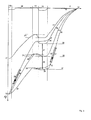
- FIG. 12 shows a schematic representation of potentials along a line AA in the semiconductor structure 100 Fig. 2 , Curve 16 shows the potential in thermodynamic equilibrium, which essentially maps the static diffusion potentials.
- the regions are characterized in the different crystal depths: 10 - top layer (top diode), which serves here as a collector of charges and control electrode; 15 - another doping region, which is called the base region of the avalanche phototransistor; 13, the floating non-depleting doping region, which serves as a hole charge emitter not directly connected to a potential; and 12 - the counter electrode of the substrate.
- the potential of the top diode is increased to the value 22.
- the curve 18 shows the corresponding course of the potential. It can be seen that the electric field strength in the upper region, near the cover layer 10 (top diode), exceeds the field strength required for an avalanche breakdown.
- a single trigger event for example, a single irradiated photon triggers an avalanche breakdown here.
- Both types of charge carriers are generated here, ie electrons and holes. The resulting holes move under the influence of the field in the direction of arrow 28 to the area of the top diode and are absorbed by this. The resulting electrons move in the direction of arrow 29 and are first collected in the further doping zone 15 (base region). This process is very fast and only takes a few picoseconds.
- the electron charges located in the base region cause a breakdown of the potential barrier formed there and, due to their presence, shift the potential there in a negative direction.
- the potential in the doping zone 13 decreases from the value 39 to the in Fig. 3 value indicated at 38.
- the semiconductor structure 100 in the front region (upper region below the cover layer 10) is again switched to the Geiger mode, regardless of how long the actual lateral outflow of the electron charges may last.
- This further outflow of the electron charges is no longer associated with an avalanche amplification of the electron charges flowing further to the substrate 12, and the hole inflow into the floating emitter region stops here self-limiting precisely if the field strength critical for the avalanche effect is undershot in the rear region.
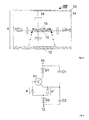
- Fig. 5 The equivalent circuit diagram in Fig. 5 is therefore only simplified because existing coupling capacitances to the neighboring pixels are omitted here for the sake of simplicity of illustration.
- D1 denote the avalanche diode in the upper part of the semiconductor structure 100 of a pixel at position 34
- D2 the avalanche diode in the lower part of the semiconductor structure 100 of a pixel
- C1 and C2 the capacitances to the 'floating' emitter of the bipolar transistor T1.
- the dot-line diode structures are not really present and should only indicate the first, the avalanche diode D2 of the current flowing from the base of the transistor T1 electron charges e - is supplied and there by means of avalanche multiplication resulting holes charges e + flowing into the emitter region ,
- Fig. 6 shows a schematic representation of temporal processes in connection with the above-described operations in the semiconductor structure 100.
- a single photon is absorbed in the upper avalanche diode D1 and avalanche multiplication begins.
- this phase typically 25,000 to 100,000 charge carriers of both types are generated, since the electric field strength there and at this time is greater than the field strength required for avalanche breakdown. These charge carriers are separated from the field.
- the hole charges flow into the top diode, the electron charges into the further doping region 15 (base region). This happens within a few picoseconds.
- the potential of the barrier between the further doping region 15 and the floating doping region 13 (emitter region) is then reduced, and further hole charges are started, which are stored on the capacitors C1, C2 are to flow to the top layer 10 formed with the top layer.
- region 46 This is recorded in region 46 as a current increase.
- the total number of charge carriers flowing here depends on the current gain of the bipolar structure and is between 10... 100 and 1000. Due to the strong hole loss of the doping region 13, the potential of this region drops so far that the avalanche process in D1 stops comes. In addition, a large part of the electron charges generated in the base region 15 by the multiplication will recombine here. This process is also very fast and requires only a few more picoseconds.
- the barrier between the further doping region 15 and the doping region 13 becomes larger and the current flow to the top diode breaks down as shown in the region 47.
- the further doping region 15 (base) are now only relatively few electron charges, which can flow only on the side of a pixel.
- the first electron charges flowing out to the substrate 12 now start the second avalanche process in the lower diode D2. This process is also very fast, and in the period 48 the hole charge on the emitter capacitances C1, C2 is renewed thereby bringing the entire structure back into the photoperiod-ready Geiger mode of the upper avalanche diode D1.
- the barrier height adjusts itself via the outflow of electrons to the then n-type top diode. These electrons then very likely cause another avalanche breakdown, which is falsely attributed to 'afterpulsing' imaginary radiating photons from neighboring pixels.
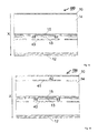
- Fig. 7 and 8th each show a schematic representation of a semiconductor structure 100 in section, wherein embodiments for different lateral extensions of the further doping regions 15 are shown.
- a problem that may arise for the first time with the use of high-resistance semiconductor substrates 14 can be avoided.
- the 'floating' emitter regions (doping region 13) as they are with 26 and 27 in Fig. 3 can be shown and are required for the operation, there may be problems with the fact that the realized exclusively by the low doping in the gap areas potential barriers for hole charges between two directly adjacent emitter regions (doping regions 13) are degraded so far as the holes to flow between them kick off. A whole-area further doping zone 15 in the entire pixel region can effectively prevent this.
- shifted implantation depth of the further doping zone 15 is an operating point adjustment of the doping concentrations possible. Since in the region lying directly above the emitter regions 13 parts of the n-type doping of the further doping zone 15 are compensated by the much higher p-type doping of the doping region 13, it is possible to have a smaller doping concentration there to realize in the gaps. On the one hand, a sufficient potential barrier in the base region is set, on the other hand the potential barrier for the separation of directly adjacent emitter regions in the gap regions is intensified.
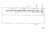
- Fig. 11 shows a schematic representation of a semiconductor structure 100 with additional upper doping regions 41.
- the region of high field strength (high field, Avalanch region) is limited to a region 42 below the cover layer 10.
- Fig. 12 1 shows a schematic illustration of a semiconductor structure 100 with additional lower doping regions 43. With the aid of the additional lower doping regions 43, the quenching region is limited to a region 44 below the doping regions 13.
- Fig. 13 shows a schematic representation of a semiconductor structure 100 with additional upper and lower doping regions 41, 43.
- Fig. 11 shown structure used near the surface. This results in two series-connected avalanche structures, which are coupled to each other via a bipolar transistor construction with floating emitter.
- the goal is often to make the pixel geometries larger to limit the problems of afterpulsing .
- This requires smaller structural capacities.
- the total layer thicknesses to be depleted between the cap layer 10 and the substrate 12 become quite large, there may be problems such that the avalanche field required to restore the potential of the emitters is difficult to be achieved in the lower part of the structure. Therefore, here as well, the avalanche region can be restricted to the regions marked 44 by means of the n-type doping zone 43. The entire required working point voltage is thus further reduced.
- the potential in the central region of the structure the potential is large enough to be able to use the avalanche effect of the D2 diode for resetting, and not in the edge regions of the same detector due to the high-impedance coupling of the hole charges to the edge regions. In fact, hardly any of the required high potentials are reached there. Of course, the very fast times of active restoring in the central area and the much slower ones from the peripheral areas are mixed together here.
- a novel semiconductor detector was introduced, which describes the coupling of avalanche regions with the construction of a bipolar transistor. This achieves very fast active "quenching" in each individual pixel.
Landscapes
- Light Receiving Elements (AREA)
- Measurement Of Radiation (AREA)
- Solid State Image Pick-Up Elements (AREA)
Applications Claiming Priority (2)
| Application Number | Priority Date | Filing Date | Title |
|---|---|---|---|
| DE102012101224 | 2012-02-15 | ||
| DE102012103699A DE102012103699A1 (de) | 2012-02-15 | 2012-04-26 | Halbleiterstruktur für einen Strahlungsdetektor sowie Strahlungsdetektor |
Publications (3)
| Publication Number | Publication Date |
|---|---|
| EP2629340A2 true EP2629340A2 (fr) | 2013-08-21 |
| EP2629340A3 EP2629340A3 (fr) | 2016-07-06 |
| EP2629340B1 EP2629340B1 (fr) | 2021-04-07 |
Family
ID=47750454
Family Applications (1)
| Application Number | Title | Priority Date | Filing Date |
|---|---|---|---|
| EP13155452.9A Active EP2629340B1 (fr) | 2012-02-15 | 2013-02-15 | Structure semi-conductrice pour un détecteur de rayonnement basé sur l'effect d'avalanche ainsi que le détecteur rayonnement |
Country Status (5)
| Country | Link |
|---|---|
| US (1) | US8823124B2 (fr) |
| EP (1) | EP2629340B1 (fr) |
| JP (1) | JP6298234B2 (fr) |
| CN (1) | CN103258873B (fr) |
| DE (1) | DE102012103699A1 (fr) |
Families Citing this family (7)
| Publication number | Priority date | Publication date | Assignee | Title |
|---|---|---|---|---|
| GB2524044B (en) * | 2014-03-12 | 2019-03-27 | Teledyne E2V Uk Ltd | CMOS Image sensor |
| DE102015110484B4 (de) * | 2015-06-30 | 2023-09-28 | Infineon Technologies Austria Ag | Halbleiterbauelemente und Verfahren zum Bilden eines Halbleiterbauelements |
| JP6701135B2 (ja) * | 2016-10-13 | 2020-05-27 | キヤノン株式会社 | 光検出装置および光検出システム |
| JP7169071B2 (ja) | 2018-02-06 | 2022-11-10 | ソニーセミコンダクタソリューションズ株式会社 | 画素構造、撮像素子、撮像装置、および電子機器 |
| JP6975079B2 (ja) * | 2018-03-15 | 2021-12-01 | 株式会社東芝 | 放射線検出器 |
| JP7224823B2 (ja) * | 2018-09-19 | 2023-02-20 | キヤノン株式会社 | 光検出装置 |
| WO2020093240A1 (fr) * | 2018-11-06 | 2020-05-14 | Shenzhen Xpectvision Technology Co., Ltd. | Détecteur de rayonnement |
Citations (2)
| Publication number | Priority date | Publication date | Assignee | Title |
|---|---|---|---|---|
| DE69011809T2 (de) | 1989-11-01 | 1995-03-09 | Philips Nv | Halbleiteranordnung und Verfahren zu ihrer Herstellung. |
| DE69721366T2 (de) | 1996-02-28 | 2004-03-25 | Hitachi, Ltd. | Diode und Stromrichterschaltungsapparat |
Family Cites Families (12)
| Publication number | Priority date | Publication date | Assignee | Title |
|---|---|---|---|---|
| NL7709618A (nl) * | 1977-09-01 | 1979-03-05 | Philips Nv | Stralingsgevoelige halfgeleiderinrichting en werkwijze ter vervaardiging daarvan. |
| CA1280196C (fr) * | 1987-07-17 | 1991-02-12 | Paul Perry Webb | Photodiode avalanche |
| US5218226A (en) * | 1989-11-01 | 1993-06-08 | U.S. Philips Corp. | Semiconductor device having high breakdown voltage |
| US7899339B2 (en) * | 2002-07-30 | 2011-03-01 | Amplification Technologies Inc. | High-sensitivity, high-resolution detector devices and arrays |
| US8519503B2 (en) * | 2006-06-05 | 2013-08-27 | Osi Optoelectronics, Inc. | High speed backside illuminated, front side contact photodiode array |
| DE102007037020B3 (de) * | 2007-08-06 | 2008-08-21 | MAX-PLANCK-Gesellschaft zur Förderung der Wissenschaften e.V. | Avalanche-Photodiode |
| DE102007045184A1 (de) * | 2007-09-21 | 2009-04-02 | Robert Bosch Gmbh | Halbleitervorrichtung und Verfahren zu deren Herstellung |
| DE102008011280B4 (de) * | 2008-02-27 | 2010-01-28 | Ketek Gmbh | Strahlungsempfangendes Halbleiterbauelement, Verfahren zum Betreiben und Verwendung desselben sowie Strahlungsdetektor und Halbleiteranordung mit dem Halbleiterbauelement |
| IT1392366B1 (it) * | 2008-12-17 | 2012-02-28 | St Microelectronics Rousset | Fotodiodo operante in modalita' geiger con resistore di soppressione integrato e controllabile, schiera di fotodiodi e relativo procedimento di fabbricazione |
| IT1393781B1 (it) * | 2009-04-23 | 2012-05-08 | St Microelectronics Rousset | Fotodiodo operante in modalita' geiger con resistore di soppressione integrato e controllabile ad effetto jfet, schiera di fotodiodi e relativo procedimento di fabbricazione |
| DE102009049793B3 (de) * | 2009-10-16 | 2011-04-07 | Silicon Sensor International Ag | Halbleiter-Photodetektor und Strahlungsdetektorsystem |
| US8779543B2 (en) * | 2011-09-19 | 2014-07-15 | Technion Research And Development Foundation Ltd. | Device having an avalanche photo diode and a method for sensing photons |
-
2012
- 2012-04-26 DE DE102012103699A patent/DE102012103699A1/de not_active Withdrawn
-
2013
- 2013-02-13 US US13/765,710 patent/US8823124B2/en not_active Expired - Fee Related
- 2013-02-14 JP JP2013026410A patent/JP6298234B2/ja not_active Expired - Fee Related
- 2013-02-15 EP EP13155452.9A patent/EP2629340B1/fr active Active
- 2013-02-18 CN CN201310052841.2A patent/CN103258873B/zh not_active Expired - Fee Related
Patent Citations (2)
| Publication number | Priority date | Publication date | Assignee | Title |
|---|---|---|---|---|
| DE69011809T2 (de) | 1989-11-01 | 1995-03-09 | Philips Nv | Halbleiteranordnung und Verfahren zu ihrer Herstellung. |
| DE69721366T2 (de) | 1996-02-28 | 2004-03-25 | Hitachi, Ltd. | Diode und Stromrichterschaltungsapparat |
Also Published As
| Publication number | Publication date |
|---|---|
| DE102012103699A1 (de) | 2013-08-22 |
| CN103258873B (zh) | 2017-06-09 |
| EP2629340B1 (fr) | 2021-04-07 |
| EP2629340A3 (fr) | 2016-07-06 |
| US8823124B2 (en) | 2014-09-02 |
| JP2013174588A (ja) | 2013-09-05 |
| US20130207216A1 (en) | 2013-08-15 |
| CN103258873A (zh) | 2013-08-21 |
| JP6298234B2 (ja) | 2018-03-20 |
Similar Documents
| Publication | Publication Date | Title |
|---|---|---|
| DE102007037020B3 (de) | Avalanche-Photodiode | |
| EP0179102B1 (fr) | Element semiconducteur appauvri avec un minimum de potentiel pour des porteurs majoritaires | |
| EP2629340B1 (fr) | Structure semi-conductrice pour un détecteur de rayonnement basé sur l'effect d'avalanche ainsi que le détecteur rayonnement | |
| DE102010000531B4 (de) | Halbleiterbauelement, elektronische Komponente und Verfahren zur Herstellung eines Halbleiterbauelements | |
| DE102007020659B4 (de) | Halbleiterbauelement und Verfahren zur Herstellung desselben | |
| DE102017129955B4 (de) | Halbleitervorrichtung mit einem barrierengebiet sowie elektrische vorrichtung | |
| DE102007018631A1 (de) | Halbleiterbauelement mit Kompensationszonen und Entladestrukturen für die Kompensationszonen | |
| DE102009038731A1 (de) | Halbleiterbauelement mit Ladungsträgerkompensationsstruktur und Verfahren zur Herstellung eines Halbleiterbauelements | |
| EP3948951B1 (fr) | Réseau de photodiodes à avalanche | |
| DE112013002352T5 (de) | Halbleitervorrichtung | |
| DE10213812A1 (de) | Leitungsüberführung für einen Halbleiter-Detektor | |
| EP2549536B1 (fr) | Structure semi-conductrice pour la détection de photons | |
| DE112021005507T5 (de) | Optischer Sensor | |
| EP2489080A2 (fr) | Photo-détecteur semi-conducteur et système de détecteur de rayonnement | |
| EP3246952A1 (fr) | Transistor mos pour circuits cmos numériques tolérants aux rayonnements | |
| DE102020114276A1 (de) | Halbleitervorrichtung | |
| DE19933162B4 (de) | Bildzelle, Bildsensor und Herstellungsverfahren hierfür | |
| EP1127379B1 (fr) | Composant a semi-conducteur de puissance a structure verticale | |
| DE112018005789T5 (de) | Esd-geschützter halbleiter-photomultiplikator | |
| EP0656659A2 (fr) | Structure de protection ESD pour circuit intégrés | |
| DE10123818A1 (de) | Anordnung mit Schutzfunktion für ein Halbleiterbauelement | |
| DE102007018367B4 (de) | Halbleiterbauelement und Verfahren zu dessen Herstellung | |
| DE102005007358B4 (de) | Lichtempfindliches Bauelement | |
| DE3427476A1 (de) | Halbleiterelement | |
| EP0892990A1 (fr) | Composant a semiconducteur a grille flottante en deux parties |
Legal Events
| Date | Code | Title | Description |
|---|---|---|---|
| PUAI | Public reference made under article 153(3) epc to a published international application that has entered the european phase |
Free format text: ORIGINAL CODE: 0009012 |
|
| AK | Designated contracting states |
Kind code of ref document: A2 Designated state(s): AL AT BE BG CH CY CZ DE DK EE ES FI FR GB GR HR HU IE IS IT LI LT LU LV MC MK MT NL NO PL PT RO RS SE SI SK SM TR |
|
| AX | Request for extension of the european patent |
Extension state: BA ME |
|
| PUAL | Search report despatched |
Free format text: ORIGINAL CODE: 0009013 |
|
| AK | Designated contracting states |
Kind code of ref document: A3 Designated state(s): AL AT BE BG CH CY CZ DE DK EE ES FI FR GB GR HR HU IE IS IT LI LT LU LV MC MK MT NL NO PL PT RO RS SE SI SK SM TR |
|
| AX | Request for extension of the european patent |
Extension state: BA ME |
|
| RIC1 | Information provided on ipc code assigned before grant |
Ipc: H01L 27/144 20060101ALI20160531BHEP Ipc: H01L 31/107 20060101AFI20160531BHEP |
|
| STAA | Information on the status of an ep patent application or granted ep patent |
Free format text: STATUS: REQUEST FOR EXAMINATION WAS MADE |
|
| 17P | Request for examination filed |
Effective date: 20170105 |
|
| RBV | Designated contracting states (corrected) |
Designated state(s): AL AT BE BG CH CY CZ DE DK EE ES FI FR GB GR HR HU IE IS IT LI LT LU LV MC MK MT NL NO PL PT RO RS SE SI SK SM TR |
|
| RAP1 | Party data changed (applicant data changed or rights of an application transferred) |
Owner name: PIERSCHEL, MICHAEL |
|
| RIN1 | Information on inventor provided before grant (corrected) |
Inventor name: PIERSCHEL, MICHAEL |
|
| STAA | Information on the status of an ep patent application or granted ep patent |
Free format text: STATUS: EXAMINATION IS IN PROGRESS |
|
| 17Q | First examination report despatched |
Effective date: 20181114 |
|
| GRAP | Despatch of communication of intention to grant a patent |
Free format text: ORIGINAL CODE: EPIDOSNIGR1 |
|
| STAA | Information on the status of an ep patent application or granted ep patent |
Free format text: STATUS: GRANT OF PATENT IS INTENDED |
|
| INTG | Intention to grant announced |
Effective date: 20201002 |
|
| GRAS | Grant fee paid |
Free format text: ORIGINAL CODE: EPIDOSNIGR3 |
|
| GRAA | (expected) grant |
Free format text: ORIGINAL CODE: 0009210 |
|
| STAA | Information on the status of an ep patent application or granted ep patent |
Free format text: STATUS: THE PATENT HAS BEEN GRANTED |
|
| AK | Designated contracting states |
Kind code of ref document: B1 Designated state(s): AL AT BE BG CH CY CZ DE DK EE ES FI FR GB GR HR HU IE IS IT LI LT LU LV MC MK MT NL NO PL PT RO RS SE SI SK SM TR |
|
| REG | Reference to a national code |
Ref country code: GB Ref legal event code: FG4D Free format text: NOT ENGLISH |
|
| REG | Reference to a national code |
Ref country code: AT Ref legal event code: REF Ref document number: 1380810 Country of ref document: AT Kind code of ref document: T Effective date: 20210415 Ref country code: CH Ref legal event code: EP |
|
| REG | Reference to a national code |
Ref country code: DE Ref legal event code: R096 Ref document number: 502013015621 Country of ref document: DE |
|
| REG | Reference to a national code |
Ref country code: IE Ref legal event code: FG4D Free format text: LANGUAGE OF EP DOCUMENT: GERMAN |
|
| REG | Reference to a national code |
Ref country code: LT Ref legal event code: MG9D |
|
| REG | Reference to a national code |
Ref country code: NL Ref legal event code: MP Effective date: 20210407 |
|
| PG25 | Lapsed in a contracting state [announced via postgrant information from national office to epo] |
Ref country code: FI Free format text: LAPSE BECAUSE OF FAILURE TO SUBMIT A TRANSLATION OF THE DESCRIPTION OR TO PAY THE FEE WITHIN THE PRESCRIBED TIME-LIMIT Effective date: 20210407 Ref country code: LT Free format text: LAPSE BECAUSE OF FAILURE TO SUBMIT A TRANSLATION OF THE DESCRIPTION OR TO PAY THE FEE WITHIN THE PRESCRIBED TIME-LIMIT Effective date: 20210407 Ref country code: NL Free format text: LAPSE BECAUSE OF FAILURE TO SUBMIT A TRANSLATION OF THE DESCRIPTION OR TO PAY THE FEE WITHIN THE PRESCRIBED TIME-LIMIT Effective date: 20210407 Ref country code: HR Free format text: LAPSE BECAUSE OF FAILURE TO SUBMIT A TRANSLATION OF THE DESCRIPTION OR TO PAY THE FEE WITHIN THE PRESCRIBED TIME-LIMIT Effective date: 20210407 Ref country code: BG Free format text: LAPSE BECAUSE OF FAILURE TO SUBMIT A TRANSLATION OF THE DESCRIPTION OR TO PAY THE FEE WITHIN THE PRESCRIBED TIME-LIMIT Effective date: 20210707 |
|
| PG25 | Lapsed in a contracting state [announced via postgrant information from national office to epo] |
Ref country code: LV Free format text: LAPSE BECAUSE OF FAILURE TO SUBMIT A TRANSLATION OF THE DESCRIPTION OR TO PAY THE FEE WITHIN THE PRESCRIBED TIME-LIMIT Effective date: 20210407 Ref country code: IS Free format text: LAPSE BECAUSE OF FAILURE TO SUBMIT A TRANSLATION OF THE DESCRIPTION OR TO PAY THE FEE WITHIN THE PRESCRIBED TIME-LIMIT Effective date: 20210807 Ref country code: GR Free format text: LAPSE BECAUSE OF FAILURE TO SUBMIT A TRANSLATION OF THE DESCRIPTION OR TO PAY THE FEE WITHIN THE PRESCRIBED TIME-LIMIT Effective date: 20210708 Ref country code: SE Free format text: LAPSE BECAUSE OF FAILURE TO SUBMIT A TRANSLATION OF THE DESCRIPTION OR TO PAY THE FEE WITHIN THE PRESCRIBED TIME-LIMIT Effective date: 20210407 Ref country code: RS Free format text: LAPSE BECAUSE OF FAILURE TO SUBMIT A TRANSLATION OF THE DESCRIPTION OR TO PAY THE FEE WITHIN THE PRESCRIBED TIME-LIMIT Effective date: 20210407 Ref country code: ES Free format text: LAPSE BECAUSE OF FAILURE TO SUBMIT A TRANSLATION OF THE DESCRIPTION OR TO PAY THE FEE WITHIN THE PRESCRIBED TIME-LIMIT Effective date: 20210407 Ref country code: PT Free format text: LAPSE BECAUSE OF FAILURE TO SUBMIT A TRANSLATION OF THE DESCRIPTION OR TO PAY THE FEE WITHIN THE PRESCRIBED TIME-LIMIT Effective date: 20210809 Ref country code: PL Free format text: LAPSE BECAUSE OF FAILURE TO SUBMIT A TRANSLATION OF THE DESCRIPTION OR TO PAY THE FEE WITHIN THE PRESCRIBED TIME-LIMIT Effective date: 20210407 Ref country code: NO Free format text: LAPSE BECAUSE OF FAILURE TO SUBMIT A TRANSLATION OF THE DESCRIPTION OR TO PAY THE FEE WITHIN THE PRESCRIBED TIME-LIMIT Effective date: 20210707 |
|
| REG | Reference to a national code |
Ref country code: DE Ref legal event code: R097 Ref document number: 502013015621 Country of ref document: DE |
|
| PG25 | Lapsed in a contracting state [announced via postgrant information from national office to epo] |
Ref country code: RO Free format text: LAPSE BECAUSE OF FAILURE TO SUBMIT A TRANSLATION OF THE DESCRIPTION OR TO PAY THE FEE WITHIN THE PRESCRIBED TIME-LIMIT Effective date: 20210407 Ref country code: CZ Free format text: LAPSE BECAUSE OF FAILURE TO SUBMIT A TRANSLATION OF THE DESCRIPTION OR TO PAY THE FEE WITHIN THE PRESCRIBED TIME-LIMIT Effective date: 20210407 Ref country code: EE Free format text: LAPSE BECAUSE OF FAILURE TO SUBMIT A TRANSLATION OF THE DESCRIPTION OR TO PAY THE FEE WITHIN THE PRESCRIBED TIME-LIMIT Effective date: 20210407 Ref country code: DK Free format text: LAPSE BECAUSE OF FAILURE TO SUBMIT A TRANSLATION OF THE DESCRIPTION OR TO PAY THE FEE WITHIN THE PRESCRIBED TIME-LIMIT Effective date: 20210407 Ref country code: SM Free format text: LAPSE BECAUSE OF FAILURE TO SUBMIT A TRANSLATION OF THE DESCRIPTION OR TO PAY THE FEE WITHIN THE PRESCRIBED TIME-LIMIT Effective date: 20210407 Ref country code: SK Free format text: LAPSE BECAUSE OF FAILURE TO SUBMIT A TRANSLATION OF THE DESCRIPTION OR TO PAY THE FEE WITHIN THE PRESCRIBED TIME-LIMIT Effective date: 20210407 |
|
| PLBE | No opposition filed within time limit |
Free format text: ORIGINAL CODE: 0009261 |
|
| STAA | Information on the status of an ep patent application or granted ep patent |
Free format text: STATUS: NO OPPOSITION FILED WITHIN TIME LIMIT |
|
| 26N | No opposition filed |
Effective date: 20220110 |
|
| PG25 | Lapsed in a contracting state [announced via postgrant information from national office to epo] |
Ref country code: IS Free format text: LAPSE BECAUSE OF FAILURE TO SUBMIT A TRANSLATION OF THE DESCRIPTION OR TO PAY THE FEE WITHIN THE PRESCRIBED TIME-LIMIT Effective date: 20210807 Ref country code: AL Free format text: LAPSE BECAUSE OF FAILURE TO SUBMIT A TRANSLATION OF THE DESCRIPTION OR TO PAY THE FEE WITHIN THE PRESCRIBED TIME-LIMIT Effective date: 20210407 |
|
| PG25 | Lapsed in a contracting state [announced via postgrant information from national office to epo] |
Ref country code: IT Free format text: LAPSE BECAUSE OF FAILURE TO SUBMIT A TRANSLATION OF THE DESCRIPTION OR TO PAY THE FEE WITHIN THE PRESCRIBED TIME-LIMIT Effective date: 20210407 |
|
| REG | Reference to a national code |
Ref country code: DE Ref legal event code: R119 Ref document number: 502013015621 Country of ref document: DE |
|
| PG25 | Lapsed in a contracting state [announced via postgrant information from national office to epo] |
Ref country code: MC Free format text: LAPSE BECAUSE OF FAILURE TO SUBMIT A TRANSLATION OF THE DESCRIPTION OR TO PAY THE FEE WITHIN THE PRESCRIBED TIME-LIMIT Effective date: 20210407 |
|
| REG | Reference to a national code |
Ref country code: CH Ref legal event code: PL |
|
| REG | Reference to a national code |
Ref country code: BE Ref legal event code: MM Effective date: 20220228 |
|
| GBPC | Gb: european patent ceased through non-payment of renewal fee |
Effective date: 20220215 |
|
| PG25 | Lapsed in a contracting state [announced via postgrant information from national office to epo] |
Ref country code: LU Free format text: LAPSE BECAUSE OF NON-PAYMENT OF DUE FEES Effective date: 20220215 |
|
| PG25 | Lapsed in a contracting state [announced via postgrant information from national office to epo] |
Ref country code: FR Free format text: LAPSE BECAUSE OF NON-PAYMENT OF DUE FEES Effective date: 20220228 |
|
| PG25 | Lapsed in a contracting state [announced via postgrant information from national office to epo] |
Ref country code: LI Free format text: LAPSE BECAUSE OF NON-PAYMENT OF DUE FEES Effective date: 20220228 Ref country code: IE Free format text: LAPSE BECAUSE OF NON-PAYMENT OF DUE FEES Effective date: 20220215 Ref country code: GB Free format text: LAPSE BECAUSE OF NON-PAYMENT OF DUE FEES Effective date: 20220215 Ref country code: DE Free format text: LAPSE BECAUSE OF NON-PAYMENT OF DUE FEES Effective date: 20220901 Ref country code: CH Free format text: LAPSE BECAUSE OF NON-PAYMENT OF DUE FEES Effective date: 20220228 |
|
| PG25 | Lapsed in a contracting state [announced via postgrant information from national office to epo] |
Ref country code: BE Free format text: LAPSE BECAUSE OF NON-PAYMENT OF DUE FEES Effective date: 20220228 |
|
| REG | Reference to a national code |
Ref country code: AT Ref legal event code: MM01 Ref document number: 1380810 Country of ref document: AT Kind code of ref document: T Effective date: 20220215 |
|
| PG25 | Lapsed in a contracting state [announced via postgrant information from national office to epo] |
Ref country code: AT Free format text: LAPSE BECAUSE OF NON-PAYMENT OF DUE FEES Effective date: 20220215 |
|
| PG25 | Lapsed in a contracting state [announced via postgrant information from national office to epo] |
Ref country code: HU Free format text: LAPSE BECAUSE OF FAILURE TO SUBMIT A TRANSLATION OF THE DESCRIPTION OR TO PAY THE FEE WITHIN THE PRESCRIBED TIME-LIMIT; INVALID AB INITIO Effective date: 20130215 |
|
| PG25 | Lapsed in a contracting state [announced via postgrant information from national office to epo] |
Ref country code: MK Free format text: LAPSE BECAUSE OF FAILURE TO SUBMIT A TRANSLATION OF THE DESCRIPTION OR TO PAY THE FEE WITHIN THE PRESCRIBED TIME-LIMIT Effective date: 20210407 Ref country code: CY Free format text: LAPSE BECAUSE OF FAILURE TO SUBMIT A TRANSLATION OF THE DESCRIPTION OR TO PAY THE FEE WITHIN THE PRESCRIBED TIME-LIMIT Effective date: 20210407 |
|
| PG25 | Lapsed in a contracting state [announced via postgrant information from national office to epo] |
Ref country code: MT Free format text: LAPSE BECAUSE OF FAILURE TO SUBMIT A TRANSLATION OF THE DESCRIPTION OR TO PAY THE FEE WITHIN THE PRESCRIBED TIME-LIMIT Effective date: 20210407 |
|
| PG25 | Lapsed in a contracting state [announced via postgrant information from national office to epo] |
Ref country code: TR Free format text: LAPSE BECAUSE OF FAILURE TO SUBMIT A TRANSLATION OF THE DESCRIPTION OR TO PAY THE FEE WITHIN THE PRESCRIBED TIME-LIMIT Effective date: 20210407 |