EP2629358B1 - Phasenverschieber und antenne - Google Patents
Phasenverschieber und antenne Download PDFInfo
- Publication number
- EP2629358B1 EP2629358B1 EP12732391.3A EP12732391A EP2629358B1 EP 2629358 B1 EP2629358 B1 EP 2629358B1 EP 12732391 A EP12732391 A EP 12732391A EP 2629358 B1 EP2629358 B1 EP 2629358B1
- Authority
- EP
- European Patent Office
- Prior art keywords
- coupling arm
- arc conductor
- arc
- conductor
- phase shifter
- Prior art date
- Legal status (The legal status is an assumption and is not a legal conclusion. Google has not performed a legal analysis and makes no representation as to the accuracy of the status listed.)
- Active
Links
Images




Classifications
-
- H—ELECTRICITY
- H01—ELECTRIC ELEMENTS
- H01P—WAVEGUIDES; RESONATORS, LINES, OR OTHER DEVICES OF THE WAVEGUIDE TYPE
- H01P1/00—Auxiliary devices
- H01P1/18—Phase-shifters
- H01P1/184—Strip line phase-shifters
Definitions
- Embodiments of the present invention relate to the field of wireless communications technologies, and in particular, to a phase shifter and an antenna.
- a phase shifter may control a change of a signal phase, and is a key component in an antenna of a wireless communication base station.
- a phase shifter By using a phase shifter, a phase of an input signal may be shifted, a relative phase of a signal between antenna units may be changed, and a downtilt angle of an antenna beam may be adjusted, so as to facilitate the optimization of a communication network.
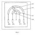
- FIG. 1 is a schematic structural diagram of a phase shifter in the prior art.
- the phase shifter provided in the prior art includes a first arc conductor 101 and a second arc conductor 102, where the first arc conductor 101 and the second arc conductor 102 are concentrically disposed; and a coupling arm 103, which is a physically integrated structure, and laps over the first arc conductor 101 and the second arc conductor 102, where a capacitive coupling electrical connection is formed at a lapping position between the coupling arm 103 and each arc conductor.
- the signals are coupled to the first arc conductor 101 and the second arc conductor 102 along the coupling arm 103, the signal coupled to the first arc conductor 101 is output from a first output end 1011 and a second output end 1012 of the first arc conductor 101, and the signal coupled to the second arc conductor 102 is output from a third output end 1021 and a fourth output end 1022 of the second arc conductor 102.
- a lapping position between the first arc conductor 101 and the coupling arm 103 and a lapping position between the second arc conductor 102 and the coupling arm 103 may be changed, so that a transmission path of a signal on an arc conductor is changed, and signals with opposite phases are output from two ends of the arc conductor, thereby implementing phase shift of the signal.
- a coupling arm is an integrated structure
- the coupling arm needs to be coupled to two arc conductors at the same time, so that coupling between the two arc conductors is strong and signal interference between the arc conductors is intense.
- it is required to increase a distance between the arc conductors, which causes that the size of the phase shifter is large.
- the coupling arm is an integrated structure, to ensure that capacitive coupling is formed at a lapping position between the coupling arm and each of the two arc conductors, high manufacturing precision is required for the coupling arm, which leads to a high manufacture cost of the phase shifter.
- FR2930078 discloses a rotary phase shifting device for panel type antenna in mobile telephone network.
- the device has upper and lower conductive pieces displaced in rotation around a longitudinal axis with respect to an electrically conductive strip (81). Lower and upper layers made of dielectric material, are arranged on both sides of the strip.
- Each conductive piece has a rotary arm (83) rotated around the axis.
- the arm has a distal end provided with a coupling zone (84) that partially covers the strip.
- the zone has a covering surface extended from a side of the arm. The covering surface is larger than a covering surface extended from an opposite side of the arm.
- Embodiments of the present invention provide a phase shifter and an antenna, which may effectively solve problems that coupling between arc conductors in an existing phase shifter in which a coupling arm is an integrated structure is strong and a manufacture cost is high.
- An embodiment of the present invention provides a phase shifter, including an arc conductor component and a coupling arm component swingably disposed along the arc conductor component, where the arc conductor component includes:
- An embodiment of the present invention provides an antenna, including a phase shifter, where each output end of the phase shifter is connected to an antenna unit; and the phase shifter adopts a phase shifter provided in the foregoing embodiment of the present invention.
- a first coupling arm and a second coupling arm of a coupling arm component are disposed in a spatially isolated manner and the first coupling arm and the second coupling arm lap over a first arc conductor at different positions, so that coupling between the first arc conductor and a second arc conductor may be effectively reduced, signal interference between the arc conductors is avoided, the precision of an output signal of the phase shifter is improved, and at the same time, the size of the phase shifter is effectively decreased, and manufacture costs of the phase shifter and the antenna are reduced.
- the embodiments of the present invention provide a phase shifter, so as to implement signal transmission between arc conductors by using separately disposed coupling arms.
- the phase shifter specifically includes an arc conductor component and a coupling arm component that is swingably disposed along the arc conductor component.
- the arc conductor component includes a first arc conductor and a second arc conductor that are concentrically disposed, where a radius of the first arc conductor is smaller than that of the second arc conductor.
- the coupling arm component includes a first coupling arm and a second coupling arm that are disposed in a spatially isolated manner.
- a first end of the first coupling arm laps over the first arc conductor, and a second end of the first coupling arm is used to connect an input signal.
- a first end of the second coupling arm laps over the first arc conductor, and a second end of the second coupling arm laps over the second arc conductor.
- the first coupling arm and the second coupling arm lap over the first arc conductor at different positions, and a capacitive coupling electrical connection is formed at a lapping position between each coupling arm and each arc conductor.
- the first coupling arm and the second coupling arm are separate structures disposed in a spatially isolated manner and lap over the first arc conductor at different positions.
- the input signal at the second end of the first coupling arm is first coupled to the first arc conductor through the first coupling arm, then coupled from the first arc conductor to the second coupling arm, and finally coupled from the second coupling arm to the second arc conductor, so that coupling between the first arc conductor and the second arc conductor may be smaller, so as to decrease signal interference between the arc conductors and improve the performance of the phase shifter. Meanwhile, a shorter distance between the first arc conductor and the second arc conductor may be set to reduce the size of the phase shifter.
- first coupling arm and the second coupling arm are disposed as separate structures disposed in a spatially isolated manner, so that manufacture complexity of a coupling arm is simplified, coupling precision between the coupling arm and the arc conductor is more easily controlled, and a manufacture cost of the phase shifter is reduced.
- first end of the first coupling arm may include at least two lapping portions, and the first coupling arm may lap over the first arc conductor at different positions through the at least two lapping portions.
- first end of the second coupling arm may also include at least two lapping portions, and the second coupling arm may lap over the first arc conductor at different positions through the at least two lapping portions.
- second end of the second coupling arm may also include at least two lapping portions, and the second coupling arm may lap over the second arc conductor at different positions through the at least two lapping portions.
- swingable disposition of the coupling arm component along the arc conductor component indicates that, the coupling arm component may be disposed in a manner of being rotatable around the center of the arc conductors in the arc conductor component, so that the coupling arm component may rotate and swing along the arc conductor component when rotating around the center.
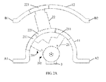
- FIG. 2A is a front view of a phase shifter according to a first embodiment of the present invention
- FIG. 2B is a schematic diagram of an assembly structure of the phase shifter according to the first embodiment of the present invention.
- the phase shifter according to this embodiment of the present invention is a four-port phase shifter.
- an arc conductor component 1 in the phase shifter includes a first arc conductor 11 and a second arc conductor 12, where the first arc conductor 11 and the second arc conductor 12 are concentrically disposed, and a radius of the first arc conductor 11 is smaller than that of the second arc conductor 12.
- a coupling arm component 2 includes a first coupling arm 21 and a second coupling arm 22.
- a first end 201 of the first coupling arm 21 laps over the first arc conductor 11, and a second end 202 of the first coupling arm 21 serves as an input end for inputting a signal and is used to connect an input signal.
- a first end of the second coupling arm 22 laps over the first arc conductor 11, and a second end of the second coupling arm 22 laps over the second arc conductor 12.
- a capacitive coupling electrical connection may be formed through the lapping between each coupling arm and each arc conductor, so that the input signal connected by the second end 202 of the first coupling arm 21 may be transmitted to end portions of each arc conductor through the capacitive coupling electrical connection formed at a lapping position between the coupling arm and the arc conductor.
- output ends A1 and A2 are disposed at two ends of the first arc conductor 11 respectively, and output ends B1 and B2 are disposed at two ends of the second arc conductor 12 respectively, where A1 and B1 are located at the same side, and A2 and B2 are located at the same side.
- the input signal input through the second end 202 of the first coupling arm 21 may be output as a signal with a certain phase from the four output ends.
- the first end 201 of the first coupling arm 21 may lap over the first arc conductor 11 through two or more lapping portions.
- the first end 201 of the first coupling arm 21 has two first lapping portions 211, where the two first lapping portions 211 may be disposed symmetrically and each lap over the first arc conductor 11, and the two first lapping portions 211 are located on the first arc conductor 11 at different positions.
- the input signal input from the second end 202 of the first coupling arm 21 may be coupled to the first arc conductor 11 through the two first lapping portions 211 and be output from the two ends A1 and A2 of the first arc conductor 11.
- one lapping portion 221 is disposed at each of the two ends of the second coupling arm 22, and the two lapping portions 221 lap over the first arc conductor 11 and the second arc conductor 12 respectively.
- the lapping portion 221 that laps over the first arc conductor 11 and the two first lapping portions 211 on the first coupling arm 21 are located on the first arc conductor 11 at different positions, so that the first coupling arm 21 and the second coupling arm 22 are disposed in a spatially isolated manner.
- the two first lapping portions 211 on the first end 201 of the first coupling arm 21 may be symmetrically disposed relative to the lapping portion 221.
- a signal coupled to the first arc conductor 11 through the first coupling arm 21 is coupled to the second coupling arm 22 at the lapping portion 221 of the first arc conductor 11, finally coupled, through the second coupling arm 22, to the second arc conductor 12 at the lapping portion 221 that is located on the second arc conductor 12, and output from the two ends B1 and B2 of the second arc conductor 12.
- the arc conductor component 1 may be disposed on a first substrate 10, the coupling arm component 2 is disposed on a second substrate 20, and the first substrate 10 and the second substrate 20 are connected through a pivot 30 that is located at the center position of the first arc conductor 11, so that the second substrate 20 may swing around the pivot 30 along the first substrate 10 and drive the coupling arm component 2 to swing along the arc conductor component 1.
- a lapping position between each coupling arm and each arc conductor may be changed, thereby implementing phase shift of a signal.
- phases of signals output from the two ends of each arc conductor can be controlled and adjusted, thereby implementing adjustment of output phases.
- the first substrate 10 and the second substrate 20 are folded and are connected through the pivot 30, so as to form a phase shifter.
- the first substrate 10 and the second substrate 20 may be connected in other manners.
- a blind hole may be disposed at the center position of the first arc conductor 11 on the first substrate 10, and a positioning column may be disposed at a corresponding position on the second substrate 20; therefore, the second substrate 20 can swing along the first substrate 10 through coordination between the positioning column and the blind hole.
- concentric disposition of the first arc conductor and the second arc conductor indicates that the center positions of the two arc conductors overlap completely or are close to each other, for example, with a distance being less than 1 mm.
- connection of the first substrate and the second substrate through the pivot that is disposed at the center position of the first arc conductor indicates that the pivot is disposed at or near the center position of the first arc conductor.
- disposition of the first coupling arm and the second coupling arm in a spatially isolated manner indicates that the first coupling arm and the second coupling arm are physically separate structures.
- the first substrate 10 and the second substrate 20 are printed circuit boards (Printed Circuit Board, PCB), where the arc conductor component 1 and the coupling arm component 2 are metal wires printed on the PCBs.
- the first arc conductor 11 and the second arc conductor 12 are metal arc strips formed on the PCB that serves as the first substrate 10
- the first coupling arm 21 and the second coupling arm 22 are metal strips formed on the PCB that serves as the second substrate 20.
- Each metal arc strip and each metal strip may form a circuit with a microstrip structure, so as to implement signal transmission in the circuit.
- phase shifter By forming a required arc conductor and coupling arm on a PCB, a cost of the phase shifter may be effectively reduced, on the basis that the same function of an conventional phase shifter is implemented; moreover, the phase shifter may have a smaller size, so that an integration level is higher when the phase shifter is connected to another component.
- the metal arc strip and the metal strip may be fabricated by using an etching process, so as to obtain a metal wire structure with a required shape.
- the formed arc conductors or coupling arms may also be a strip line structure, which is not limited in this embodiment.
- a signal input conductor portion 3 may further be disposed on the first substrate 10 and is used to connect an input signal.
- the second end 202 of the first coupling arm 21 laps over the signal input conductor portion 3.
- the signal input conductor portion 3 is a circular metal wire printed on the PCB that serves as the first substrate 10.
- the circular metal wire laps over a corresponding position of the metal strip that is printed on the second substrate 20 and serves as the first coupling arm 21, and a capacitive coupling electrical connection is formed at a lapping position.
- the input signal input from the signal input conductor portion 3 may be coupled to the first coupling arm 21 through the capacitive coupling electrical connection at a lapping position between the signal input conductor portion 3 and the first coupling arm 21, then coupled from the first coupling arm 21 to the first arc conductor 11 and coupled from the first arc conductor 11 to the second coupling arm 22, and finally coupled from the second coupling arm 22 to the second arc conductor 12.
- green oil may be coated or an isolation film made of a nonmetallic material may be added on the coupling arm and the arc conductor, so as to ensure that a capacitive coupling electrical connection between the coupling arm and the arc conductor is formed at a lapping position.
- the lapping position between the first coupling arm 21 and the first arc conductor 11 moves along the arc conductors with the swinging.
- the input signal input from the signal input conductor portion 3 may form an output signal with a certain phase at each of the two ends of the first arc conductor and the second arc conductor, where phase change trends of output signals from the two ends of the same arc conductor are opposite, and phase change trends of output signals from the output ends of the two arc conductors at the same side are the same.
- the output ends A1 and A2 of the first arc conductor 11 output the output signals with opposite phase change trends
- the output ends B1 and B2 of the second arc conductor also output the output signals with opposite phase change trends
- A1 and B1 output the output signals with the same phase change trend.
- phase variation amounts of signals output by output ends of different arc conductors may be determined by radiuses of the arc conductors, and therefore, arc conductors with proper radiuses may be disposed according to an actual requirement.
- each lapping portion that is on each coupling arm and is used to lap over each arc conductor is an arc structure having the same shape as that of the arc conductor, that is, at a lapping position between a coupling arm and an arc conductor, a lapping portion of the coupling arm has the same shape as that of the arc conductor, and in this way, performance of a capacitive coupling electrical connection formed at the lapping position between the coupling arm and the arc conductor may be better.
- coupling arms are disposed as separate structures in an isolated manner, so that an input signal is coupled to a first arc conductor through a first coupling arm, then coupled from the first arc conductor to a second coupling arm, and finally coupled from the second coupling arm to a second arc conductor, so that coupling between the first arc conductor and the second arc conductor may be smaller, signal interference between the arc conductors is avoided, and the precision of an output signal of the phase shifter is improved. Meanwhile, because the coupling between the arc conductors is weak, a distance between the arc conductors may be smaller, so that the size of the phase shifter may be decreased.
- the coupling arms are separate structures disposed in an isolated manner, it is required to ensure only the precision of a lapping position between each coupling arm and a corresponding arc conductor, and therefore, manufacture of the coupling arm is simpler, the precision is easy to be controlled, and a manufacture cost of the phase shifter is lower.
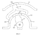
- FIG. 3 is a schematic structural diagram of a phase shifter according to a second embodiment of the present invention.
- a first end of a first coupling arm 21 has one lapping portion 212 and laps over a first arc conductor 11, and a capacitive coupling electrical connection is formed at a lapping position.
- a first end of a second coupling arm 22 has two second lapping portions 222, so that the second coupling arm 22 may lap over the first arc conductor 11 through the two second lapping portions 222. Positions of the two second lapping portions 222 on the first arc conductor 11 are different, and the two second lapping portions 222 are located at two sides of a lapping position between the first coupling arm 21 and the first arc conductor 11 and may be disposed symmetrically.
- a second end of the second coupling arm 22 has one lapping portion 221 and laps over a second arc conductor 12.
- the input signals when input signals are input from a second end 202 of the first coupling arm 21, the input signals are coupled to the first arc conductor 11 through the lapping portion 212 on the first coupling arm 21.
- One part of the signals coupled to the first arc conductor 11 are output from two ends along the first arc conductor 11; and the other part of the signals are coupled to the second coupling arm 22 through a capacitive coupling electrical connection at a lapping position between the first arc conductor 11 and the second coupling arm 22, finally coupled to the second arc conductor 12 through the lapping portion 221 on the second coupling arm 22, and output from the two ends of the second arc conductor 12 along the second arc conductor 12.
- lapping positions of the first coupling arm 21 and the second coupling arm 22 on the first arc conductor 11 and the second arc conductor 12 may be changed, and therefore, phases of the output signals at the two ends of each arc conductor may be changed.
- the first coupling arm and the second coupling arm each may also have one lapping portion when they lap over each arc conductor, as long as the lapping positions on the same arc conductor are different.
- the second end of the second coupling arm, which laps over the second arc conductor may have two or more lapping portions, so that the second coupling arm may lap over the second arc conductor through at least two lapping portions, and the at least two lapping portions correspond to different positions of the second arc conductor.
- FIG. 4 is a schematic structural diagram of a phase shifter according to a third embodiment of the present invention.
- a third arc conductor and a third coupling arm may be disposed in this embodiment, so as to form a phase shifter with six ports.
- an arc conductor component 1 may further include a third arc conductor 13.
- the third arc conductor 13 and a first arc conductor 11 are concentrically disposed, and a radius of the third arc conductor 13 is greater than that of a second arc conductor 12.
- a coupling arm component 2 may further include a third coupling arm 23.
- a first end of the third coupling arm 23 laps over the second arc conductor 12, a second end of the third coupling arm 23 laps over the third arc conductor 13 to form a capacitive coupling electrical connection at each lapping position, so that a signal is coupled from an arc conductor to a coupling arm or coupled from a coupling arm to an arc conductor through a capacitive coupling electrical connection.
- a second coupling arm 22 and the third coupling arm 23 may be a spatially and physically integrated structure. Because the signal strength of an input signal is gradually reduced after the input signal passes through a first coupling arm 21, the first arc conductor 11, and the second coupling arm 22, when the signal is coupled to the second arc conductor 12 and the third arc conductor 13 respectively through the second coupling arm 22 and the third coupling arm 23 that are an integrated structure, coupling between the second arc conductor 12 and the third arc conductor 13 is smaller and signal interference between the two arc conductors is weaker, which does not affect the precision of the phase shifter.
- input signals input from a second end 202 of the first coupling arm 21 may be coupled to the first arc conductor 11 through the first coupling arm 21.
- Part of the signals are output from two ends of the first arc conductor 11 and phase change trends of the signals output from the two ends are opposite, and part of the signals are coupled to the second coupling arm 22.
- One part of the signals coupled to the second coupling arm 22 are coupled to the second arc conductor 12, and one part of the signals are coupled to the third arc conductor 13.
- the signals coupled to the second arc conductor 12 are output from two ends of the second arc conductor 12, the signals coupled to the third arc conductor 13 are output from two ends of the third arc conductor 13, and phase change trends of the signals output from the two ends of each arc conductor are opposite.
- FIG. 5 is a schematic structural diagram of a phase shifter according to a fourth embodiment of the present invention.
- a difference from the technical solution in the embodiment shown in FIG. 4 lies in that, in this embodiment, there is only one lapping portion at which a first coupling arm laps over a first arc conductor, while a second coupling arm laps over the first arc conductor through two second lapping portions.
- a first end of a first coupling arm 21 has one lapping portion 212 and laps over a first arc conductor 11, and a capacitive coupling electrical connection is formed at a lapping position.
- a first end of a second coupling arm 22 has two second lapping portions 222, so that the second coupling arm 22 may lap over the first arc conductor 11 through the two second lapping portions 222. Positions of the two second lapping portions 222 on the first arc conductor 11 are different, and the two second lapping portions 222 are located at two sides of a lapping position between the first coupling arm 21 and the first arc conductor 11 and may be disposed symmetrically.
- a second end of the second coupling arm 22 has one lapping portion 221 and laps over a second arc conductor 12.
- an input signal input from a second end 202 of the first coupling arm 21 may also be first coupled to the first arc conductor 11 through the first coupling arm 21, then coupled from the first arc conductor 11 to the second coupling arm 22, and finally coupled to the second arc conductor 12 and a third arc conductor 13 from the second coupling arm 22 and a third coupling arm 23 that are an integrated structure.
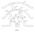
- FIG. 6 is a schematic structural diagram of a phase shifter according to a fifth embodiment of the present invention.
- a second coupling arm laps over each of a first arc conductor and a second arc conductor through two lapping portions.
- a third coupling arm and the second coupling arm are disposed in a spatially isolated manner, that is, the third coupling arm and the second coupling arm are physically separate structures. Specifically, as shown in FIG.
- two ends of a second coupling arm 22 each have two second lapping portions 222; and a lapping position between a third coupling arm 23 and a second arc conductor 12 may be located between the two second lapping portions 222 through which a second coupling arm 22 laps over the second arc conductor 12, and the two second lapping portions 222 may be disposed symmetrically.
- a signal coupled from a first arc conductor 11 to the second coupling arm 22 is first coupled to the second arc conductor 12, then coupled from the second arc conductor 12 to the third coupling arm 23, and finally coupled from the third coupling arm 23 to a third arc conductor 13.
- coupling between the arc conductors is smaller, which may be adapted to phase shift control with greater signal strength.
- each foregoing coupling arm laps over an arc conductor
- each foregoing coupling arm laps over each arc conductor through one or two lapping portions
- each foregoing coupling arm may also lap over an arc conductor through more lapping portions, for example, three or more lapping portions.
- the proper number of lapping portions may be set according to an actual requirement to lap over a corresponding arc conductor.
- phase shifter in addition to the four-port phase shifter and the six-port phase shifter, other phase shifters with the required number of ports, such as an eight-port phase shifter and a thirteen-port phase shifter, may also be implemented by increasing the number of arc conductors, and have a structure similar to that of the four-port phase shifter or the six-port phase shifter, which is not described in detail herein again.
- FIG. 7 is a schematic structural diagram of an antenna according to a sixth embodiment of the present invention.
- the antenna according to this embodiment includes a phase shifter 100, and each output end of the phase shifter 100 is connected to an antenna unit 200.
- the phase shifter 100 may adopt the phase shifter in the technical solution in the embodiment shown in FIG. 2A and FIG. 2B , which is not described in detail herein again.
- the foregoing antenna unit may be an antenna radiation unit.
- a specific structure and function of the antenna radiation unit are the same as those of an antenna radiation unit in a conventional antenna, which is not described in detail herein again.
- a phase of a signal output from an output end of each arc conductor of the phase shifter 100 may be changed by controlling a swinging position of a coupling arm in the phase shifter 100.
- a relative phase of a signal between antenna units a downtilt angle of an antenna beam is adjusted, where its specific implementation is the same as or similar to that of the conventional antenna, which is not described in detail herein again.
- the antenna according to this embodiment may also adopt the phase shifter shown in FIG. 3 .
- a phase shifter with the proper number of ports may be selected according to the number of antenna units. For example, when the antenna has six antenna units, the six-port phase shifter shown in FIG. 4 , FIG. 5 , or FIG. 6 may be selected, or the four-port phase shifter shown in FIG. 2A or FIG. 3 may be selected, and output ends of the phase shifter may be shared, which is not limited in this embodiment.
Landscapes
- Waveguide Switches, Polarizers, And Phase Shifters (AREA)
Claims (9)
- Phasenschieber, der eine bogenförmige Leiterkomponente und eine Kopplungsarmkomponente umfasst, die schwenkbar entlang der bogenförmigen Leiterkomponente angeordnet ist, wobei die bogenförmige Leiterkomponente das Folgende umfasst:einen ersten bogenförmigen Leiter (11) und einen zweiten bogenförmigen Leiter (12), die konzentrisch angeordnet sind, wobei ein Radius des ersten bogenförmigen Leiters kleiner ist als der des zweiten bogenförmigen Leiters;die Kopplungsarmkomponente umfasst einen ersten Kopplungsarm (21) und einen zweiten Kopplungsarm (22), die auf räumlich isolierte Weise angeordnet sind;ein erstes Ende (201) des ersten Kopplungsarms überlappt den ersten bogenförmigen Leiter und ein zweites Ende (202) des ersten Kopplungsarms ist ein Eingangsende zum Eingeben eines Signals;ein erstes Ende des zweiten Kopplungsarms überlappt den ersten bogenförmigen Leiter und ein zweites Ende des zweiten Kopplungsarms überlappt den zweiten bogenförmigen Leiter; undder erste Kopplungsarm und der zweite Kopplungsarm überlappen den ersten bogenförmigen Leiter an unterschiedlichen Positionen und eine kapazitiv gekoppelte elektrische Verbindung wird an einer Überlappposition zwischen jedem Kopplungsarm und jedem bogenförmigen Leiter gebildet;wobei ein Eingangssignal über den ersten Kopplungsarm (21) zu dem ersten bogenförmigen Leiter (11) gekoppelt wird, dann von dem ersten bogenförmigen Leiter (11) zu dem zweiten Kopplungsarm (22) gekoppelt wird und schließlich von dem zweiten Kopplungsarm (22) zu dem zweiten bogenförmigen Leiter (12) gekoppelt wird;wobei die bogenförmige Leiterkomponente auf einem ersten Substrat (10) angeordnet ist und die Kopplungsarmkomponente auf einem zweiten Substrat (20) angeordnet ist; undwobei das erste Substrat (10) und das zweite Substrat (20) durch eine Schwenkachse (30) verbunden sind, die an der Mittenposition des ersten bogenförmigen Leiters (11) lokalisiert ist, und wobei die Kopplungsarmkomponente dafür ausgelegt ist, entlang dem bogenförmigen Leiter durch die Schwenkachse (30) zu schwenken.
- Phasenschieber nach Anspruch 1, wobei das erste Ende des ersten Kopplungsarms mindestens zwei Überlappteile (211) umfasst und der erste Kopplungsarm den ersten bogenförmigen Leiter an unterschiedlichen Positionen mit den mindestens zwei Überlappteilen überlappt; wobei das erste Ende (221) des zweiten Kopplungsarms zwischen den mindestens zwei Überlappteilen (211) des ersten Kopplungsarms liegt.
- Phasenschieber nach Anspruch 1, wobei das erste Ende des zweiten Kopplungsarms mindestens zwei Überlappteile (222) umfasst und der zweite Kopplungsarm den ersten bogenförmigen Leiter an unterschiedlichen Positionen mit den mindestens zwei Überlappteilen überlappt; wobei das erste Ende (212) des ersten Kopplungsarms zwischen den mindestens zwei Überlappteilen des zweiten Kopplungsarms liegt (222).
- Phasenschieber nach einem der Ansprüche 1 bis 3, wobei die bogenförmige Leiterkomponente ferner mindestens einen dritten bogenförmigen Leiter (13) umfasst;
der dritte bogenförmige Leiter und der erste bogenförmige Leiter sind konzentrisch angeordnet und ein Radius des dritten bogenförmigen Leiters ist größer als der des zweiten bogenförmigen Leiters;
die Kopplungsarmkomponente umfasst ferner einen dritten Kopplungsarm (23); und ein erstes Ende des dritten Kopplungsarms überlappt den zweiten bogenförmigen Leiter und ein zweites Ende des dritten Kopplungsarms überlappt den dritten bogenförmigen Leiter;
das Eingangssignal wird zu dem dritten Kopplungsarm (23) und schließlich von dem dritten Kopplungsarm (23) zu dem dritten bogenförmigen Leiter (13) gekoppelt. - Phasenschieber nach Anspruch 4, wobei der zweite Kopplungsarm und der dritte Kopplungsarm auf räumlich isolierte Weise angeordnet sind.
- Phasenschieber nach Anspruch 1, wobei ein Signaleingangsleiterteil ferner auf dem ersten Substrat angeordnet ist; und
das zweite Ende des ersten Kopplungsarms das Signaleingangsleiterteil überlappt und das Signaleingangsleiterteil ein Eingangssignal anschließt. - Phasenschieber nach Anspruch 6, wobei eine Überlappposition zwischen dem ersten Kopplungsarm und dem Signaleingangsleiterteil an der Mittenposition des ersten bogenförmigen Leiters lokalisiert ist; und
eine kapazitiv gekoppelte elektrische Verbindung zwischen dem ersten Kopplungsarm und dem Signaleingangsleiterteil an der Überlappposition gebildet wird. - Phasenschieber nach Anspruch 1, wobei sowohl das erste Substrat als auch das zweite Substrat gedruckte Schaltungsplatinen sind; und
die bogenförmige Leiterkomponente und die Kopplungsarmkomponente auf den gedruckten Schaltungsplatinen aufgedruckte Metalldrähte sind. - Antenne, die einen Phasenschieber umfasst, wobei jedes Ausgangsende des Phasenschiebers mit einer Antenneneinheit verbunden ist; und
der Phasenschieber einen Phasenschieber nach einem der Ansprüche 1 bis 8 annimmt.
Applications Claiming Priority (1)
| Application Number | Priority Date | Filing Date | Title |
|---|---|---|---|
| PCT/CN2012/070170 WO2012092884A2 (zh) | 2012-01-10 | 2012-01-10 | 移相器和天线 |
Publications (3)
| Publication Number | Publication Date |
|---|---|
| EP2629358A2 EP2629358A2 (de) | 2013-08-21 |
| EP2629358A4 EP2629358A4 (de) | 2014-04-09 |
| EP2629358B1 true EP2629358B1 (de) | 2015-07-29 |
Family
ID=46457744
Family Applications (1)
| Application Number | Title | Priority Date | Filing Date |
|---|---|---|---|
| EP12732391.3A Active EP2629358B1 (de) | 2012-01-10 | 2012-01-10 | Phasenverschieber und antenne |
Country Status (3)
| Country | Link |
|---|---|
| EP (1) | EP2629358B1 (de) |
| CN (1) | CN102714341B (de) |
| WO (1) | WO2012092884A2 (de) |
Cited By (1)
| Publication number | Priority date | Publication date | Assignee | Title |
|---|---|---|---|---|
| US10560856B2 (en) | 2015-08-31 | 2020-02-11 | Huawei Technologies Co., Ltd. | Phase shifter, antenna, and base station |
Families Citing this family (3)
| Publication number | Priority date | Publication date | Assignee | Title |
|---|---|---|---|---|
| US9444151B2 (en) | 2014-01-10 | 2016-09-13 | Commscope Technologies Llc | Enhanced phase shifter circuit to reduce RF cables |
| CN106374846A (zh) * | 2015-07-24 | 2017-02-01 | 中兴通讯股份有限公司 | 一种相位补偿方法及装置 |
| CN111342175B (zh) * | 2020-03-13 | 2022-02-25 | 佛山市粤海信通讯有限公司 | 一种带状线移相器和天线 |
Family Cites Families (11)
| Publication number | Priority date | Publication date | Assignee | Title |
|---|---|---|---|---|
| DE19938862C1 (de) * | 1999-08-17 | 2001-03-15 | Kathrein Werke Kg | Hochfrequenz-Phasenschieberbaugruppe |
| WO2003019720A1 (en) * | 2001-08-23 | 2003-03-06 | Ems Technologies, Inc. | Microstrip phase shifter |
| KR100562534B1 (ko) * | 2003-07-14 | 2006-03-22 | 주식회사 에이스테크놀로지 | 전력 분배 기능을 구비한 위상 가변기 |
| KR20070120281A (ko) * | 2006-06-19 | 2007-12-24 | 주식회사 케이엠더블유 | 가변 이상기 |
| JP4192190B2 (ja) * | 2006-08-23 | 2008-12-03 | 電気興業株式会社 | 移相器 |
| FR2930078B1 (fr) * | 2008-04-15 | 2011-08-26 | Alcatel Lucent | Dispositif de dephasage rotatif |
| JP2011091467A (ja) * | 2009-10-20 | 2011-05-06 | Nec Anten Corp | 分配移相器 |
| CN101807733A (zh) * | 2010-02-03 | 2010-08-18 | 东莞市晖速天线技术有限公司 | 波浪式移相器 |
| CN102005629B (zh) * | 2010-11-30 | 2013-10-09 | 广州杰赛科技股份有限公司 | 一种指针移相器 |
| CN102306872B (zh) * | 2011-07-09 | 2015-03-25 | 广州桑瑞通信设备有限公司 | 电调天线对称多路功分移相器 |
| CN102263313A (zh) * | 2011-07-27 | 2011-11-30 | 华为技术有限公司 | 一种移相装置及其应用的天线系统 |
-
2012
- 2012-01-10 WO PCT/CN2012/070170 patent/WO2012092884A2/zh not_active Ceased
- 2012-01-10 EP EP12732391.3A patent/EP2629358B1/de active Active
- 2012-01-10 CN CN2012800002082A patent/CN102714341B/zh active Active
Cited By (1)
| Publication number | Priority date | Publication date | Assignee | Title |
|---|---|---|---|---|
| US10560856B2 (en) | 2015-08-31 | 2020-02-11 | Huawei Technologies Co., Ltd. | Phase shifter, antenna, and base station |
Also Published As
| Publication number | Publication date |
|---|---|
| WO2012092884A3 (zh) | 2012-10-26 |
| WO2012092884A2 (zh) | 2012-07-12 |
| EP2629358A2 (de) | 2013-08-21 |
| EP2629358A4 (de) | 2014-04-09 |
| CN102714341B (zh) | 2013-12-04 |
| CN102714341A (zh) | 2012-10-03 |
Similar Documents
| Publication | Publication Date | Title |
|---|---|---|
| EP3703181B1 (de) | Kombinierter phasenschieber und mehrbandantennennetzwerksystem | |
| CN103534869B (zh) | 波导滤波器 | |
| CN102185180B (zh) | 移相器、天线系统及移相方法 | |
| CN108432036B (zh) | 移相器和天线 | |
| EP2629358B1 (de) | Phasenverschieber und antenne | |
| US10741898B2 (en) | Phase shifter having arc-shaped phase delay lines on opposite sides of a PCB which are adjusted by slidable parts, an antenna, and radio communications device formed therefrom | |
| WO2015161445A1 (zh) | 多极化基片集成波导天线 | |
| WO2024139746A1 (zh) | 滤波移相器及天线 | |
| CN206098723U (zh) | 一种超宽频移相器 | |
| KR101223747B1 (ko) | 안테나 위상 변위기 | |
| US20090195329A1 (en) | Variable phase shifter | |
| US20220320701A1 (en) | Coupling component, microwave device and electronic device | |
| CN101473489A (zh) | 可变移相器 | |
| US11870124B2 (en) | Balance-unbalance conversion apparatus, communications device, and communications system | |
| JP2011120050A (ja) | 無線通信端末 | |
| CN206532878U (zh) | 天线及通信设备 | |
| CN103053071A (zh) | 天线以及天线控制系统 | |
| JP2017224931A (ja) | 移相器およびアンテナ装置 | |
| WO2020189451A1 (ja) | アンテナ装置、電子機器、窓ガラス、及び移動体 | |
| KR102887275B1 (ko) | 위상 변환기 | |
| KR101077045B1 (ko) | 도전부를 이용하여 프린징 필드를 차단하는 페이즈 쉬프터 | |
| CN103187627B (zh) | 一种共面波导馈电的方向图可重构平面单极子天线 | |
| US20170346183A1 (en) | Multi-port phase shifter | |
| WO2021104069A1 (zh) | 一种射频器件 | |
| CN207818901U (zh) | 基站天线相位调节装置和基站天线 |
Legal Events
| Date | Code | Title | Description |
|---|---|---|---|
| PUAI | Public reference made under article 153(3) epc to a published international application that has entered the european phase |
Free format text: ORIGINAL CODE: 0009012 |
|
| 17P | Request for examination filed |
Effective date: 20130513 |
|
| AK | Designated contracting states |
Kind code of ref document: A2 Designated state(s): AL AT BE BG CH CY CZ DE DK EE ES FI FR GB GR HR HU IE IS IT LI LT LU LV MC MK MT NL NO PL PT RO RS SE SI SK SM TR |
|
| A4 | Supplementary search report drawn up and despatched |
Effective date: 20140306 |
|
| RIC1 | Information provided on ipc code assigned before grant |
Ipc: H01P 1/18 20060101AFI20140228BHEP |
|
| 17Q | First examination report despatched |
Effective date: 20140729 |
|
| GRAP | Despatch of communication of intention to grant a patent |
Free format text: ORIGINAL CODE: EPIDOSNIGR1 |
|
| DAX | Request for extension of the european patent (deleted) | ||
| INTG | Intention to grant announced |
Effective date: 20150206 |
|
| GRAS | Grant fee paid |
Free format text: ORIGINAL CODE: EPIDOSNIGR3 |
|
| GRAA | (expected) grant |
Free format text: ORIGINAL CODE: 0009210 |
|
| AK | Designated contracting states |
Kind code of ref document: B1 Designated state(s): AL AT BE BG CH CY CZ DE DK EE ES FI FR GB GR HR HU IE IS IT LI LT LU LV MC MK MT NL NO PL PT RO RS SE SI SK SM TR |
|
| REG | Reference to a national code |
Ref country code: GB Ref legal event code: FG4D |
|
| REG | Reference to a national code |
Ref country code: CH Ref legal event code: EP |
|
| REG | Reference to a national code |
Ref country code: AT Ref legal event code: REF Ref document number: 739924 Country of ref document: AT Kind code of ref document: T Effective date: 20150815 |
|
| REG | Reference to a national code |
Ref country code: IE Ref legal event code: FG4D |
|
| REG | Reference to a national code |
Ref country code: DE Ref legal event code: R096 Ref document number: 602012009182 Country of ref document: DE |
|
| REG | Reference to a national code |
Ref country code: FR Ref legal event code: PLFP Year of fee payment: 5 |
|
| REG | Reference to a national code |
Ref country code: AT Ref legal event code: MK05 Ref document number: 739924 Country of ref document: AT Kind code of ref document: T Effective date: 20150729 |
|
| REG | Reference to a national code |
Ref country code: LT Ref legal event code: MG4D |
|
| REG | Reference to a national code |
Ref country code: NL Ref legal event code: MP Effective date: 20150729 |
|
| PG25 | Lapsed in a contracting state [announced via postgrant information from national office to epo] |
Ref country code: GR Free format text: LAPSE BECAUSE OF FAILURE TO SUBMIT A TRANSLATION OF THE DESCRIPTION OR TO PAY THE FEE WITHIN THE PRESCRIBED TIME-LIMIT Effective date: 20151030 Ref country code: LT Free format text: LAPSE BECAUSE OF FAILURE TO SUBMIT A TRANSLATION OF THE DESCRIPTION OR TO PAY THE FEE WITHIN THE PRESCRIBED TIME-LIMIT Effective date: 20150729 Ref country code: FI Free format text: LAPSE BECAUSE OF FAILURE TO SUBMIT A TRANSLATION OF THE DESCRIPTION OR TO PAY THE FEE WITHIN THE PRESCRIBED TIME-LIMIT Effective date: 20150729 Ref country code: NO Free format text: LAPSE BECAUSE OF FAILURE TO SUBMIT A TRANSLATION OF THE DESCRIPTION OR TO PAY THE FEE WITHIN THE PRESCRIBED TIME-LIMIT Effective date: 20151029 Ref country code: LV Free format text: LAPSE BECAUSE OF FAILURE TO SUBMIT A TRANSLATION OF THE DESCRIPTION OR TO PAY THE FEE WITHIN THE PRESCRIBED TIME-LIMIT Effective date: 20150729 |
|
| PG25 | Lapsed in a contracting state [announced via postgrant information from national office to epo] |
Ref country code: ES Free format text: LAPSE BECAUSE OF FAILURE TO SUBMIT A TRANSLATION OF THE DESCRIPTION OR TO PAY THE FEE WITHIN THE PRESCRIBED TIME-LIMIT Effective date: 20150729 Ref country code: PT Free format text: LAPSE BECAUSE OF FAILURE TO SUBMIT A TRANSLATION OF THE DESCRIPTION OR TO PAY THE FEE WITHIN THE PRESCRIBED TIME-LIMIT Effective date: 20151130 Ref country code: SE Free format text: LAPSE BECAUSE OF FAILURE TO SUBMIT A TRANSLATION OF THE DESCRIPTION OR TO PAY THE FEE WITHIN THE PRESCRIBED TIME-LIMIT Effective date: 20150729 Ref country code: IS Free format text: LAPSE BECAUSE OF FAILURE TO SUBMIT A TRANSLATION OF THE DESCRIPTION OR TO PAY THE FEE WITHIN THE PRESCRIBED TIME-LIMIT Effective date: 20151129 Ref country code: HR Free format text: LAPSE BECAUSE OF FAILURE TO SUBMIT A TRANSLATION OF THE DESCRIPTION OR TO PAY THE FEE WITHIN THE PRESCRIBED TIME-LIMIT Effective date: 20150729 Ref country code: PL Free format text: LAPSE BECAUSE OF FAILURE TO SUBMIT A TRANSLATION OF THE DESCRIPTION OR TO PAY THE FEE WITHIN THE PRESCRIBED TIME-LIMIT Effective date: 20150729 Ref country code: RS Free format text: LAPSE BECAUSE OF FAILURE TO SUBMIT A TRANSLATION OF THE DESCRIPTION OR TO PAY THE FEE WITHIN THE PRESCRIBED TIME-LIMIT Effective date: 20150729 Ref country code: AT Free format text: LAPSE BECAUSE OF FAILURE TO SUBMIT A TRANSLATION OF THE DESCRIPTION OR TO PAY THE FEE WITHIN THE PRESCRIBED TIME-LIMIT Effective date: 20150729 |
|
| PG25 | Lapsed in a contracting state [announced via postgrant information from national office to epo] |
Ref country code: NL Free format text: LAPSE BECAUSE OF FAILURE TO SUBMIT A TRANSLATION OF THE DESCRIPTION OR TO PAY THE FEE WITHIN THE PRESCRIBED TIME-LIMIT Effective date: 20150729 |
|
| PG25 | Lapsed in a contracting state [announced via postgrant information from national office to epo] |
Ref country code: IT Free format text: LAPSE BECAUSE OF FAILURE TO SUBMIT A TRANSLATION OF THE DESCRIPTION OR TO PAY THE FEE WITHIN THE PRESCRIBED TIME-LIMIT Effective date: 20150729 Ref country code: CZ Free format text: LAPSE BECAUSE OF FAILURE TO SUBMIT A TRANSLATION OF THE DESCRIPTION OR TO PAY THE FEE WITHIN THE PRESCRIBED TIME-LIMIT Effective date: 20150729 Ref country code: DK Free format text: LAPSE BECAUSE OF FAILURE TO SUBMIT A TRANSLATION OF THE DESCRIPTION OR TO PAY THE FEE WITHIN THE PRESCRIBED TIME-LIMIT Effective date: 20150729 Ref country code: EE Free format text: LAPSE BECAUSE OF FAILURE TO SUBMIT A TRANSLATION OF THE DESCRIPTION OR TO PAY THE FEE WITHIN THE PRESCRIBED TIME-LIMIT Effective date: 20150729 Ref country code: SK Free format text: LAPSE BECAUSE OF FAILURE TO SUBMIT A TRANSLATION OF THE DESCRIPTION OR TO PAY THE FEE WITHIN THE PRESCRIBED TIME-LIMIT Effective date: 20150729 |
|
| REG | Reference to a national code |
Ref country code: DE Ref legal event code: R097 Ref document number: 602012009182 Country of ref document: DE |
|
| PG25 | Lapsed in a contracting state [announced via postgrant information from national office to epo] |
Ref country code: RO Free format text: LAPSE BECAUSE OF FAILURE TO SUBMIT A TRANSLATION OF THE DESCRIPTION OR TO PAY THE FEE WITHIN THE PRESCRIBED TIME-LIMIT Effective date: 20150729 Ref country code: BE Free format text: LAPSE BECAUSE OF NON-PAYMENT OF DUE FEES Effective date: 20160131 |
|
| PLBE | No opposition filed within time limit |
Free format text: ORIGINAL CODE: 0009261 |
|
| STAA | Information on the status of an ep patent application or granted ep patent |
Free format text: STATUS: NO OPPOSITION FILED WITHIN TIME LIMIT |
|
| 26N | No opposition filed |
Effective date: 20160502 |
|
| PG25 | Lapsed in a contracting state [announced via postgrant information from national office to epo] |
Ref country code: LU Free format text: LAPSE BECAUSE OF FAILURE TO SUBMIT A TRANSLATION OF THE DESCRIPTION OR TO PAY THE FEE WITHIN THE PRESCRIBED TIME-LIMIT Effective date: 20160110 Ref country code: SI Free format text: LAPSE BECAUSE OF FAILURE TO SUBMIT A TRANSLATION OF THE DESCRIPTION OR TO PAY THE FEE WITHIN THE PRESCRIBED TIME-LIMIT Effective date: 20150729 |
|
| REG | Reference to a national code |
Ref country code: CH Ref legal event code: PL |
|
| PG25 | Lapsed in a contracting state [announced via postgrant information from national office to epo] |
Ref country code: MC Free format text: LAPSE BECAUSE OF FAILURE TO SUBMIT A TRANSLATION OF THE DESCRIPTION OR TO PAY THE FEE WITHIN THE PRESCRIBED TIME-LIMIT Effective date: 20150729 |
|
| PG25 | Lapsed in a contracting state [announced via postgrant information from national office to epo] |
Ref country code: CH Free format text: LAPSE BECAUSE OF NON-PAYMENT OF DUE FEES Effective date: 20160131 Ref country code: LI Free format text: LAPSE BECAUSE OF NON-PAYMENT OF DUE FEES Effective date: 20160131 |
|
| REG | Reference to a national code |
Ref country code: IE Ref legal event code: MM4A |
|
| REG | Reference to a national code |
Ref country code: FR Ref legal event code: PLFP Year of fee payment: 6 |
|
| PG25 | Lapsed in a contracting state [announced via postgrant information from national office to epo] |
Ref country code: BE Free format text: LAPSE BECAUSE OF FAILURE TO SUBMIT A TRANSLATION OF THE DESCRIPTION OR TO PAY THE FEE WITHIN THE PRESCRIBED TIME-LIMIT Effective date: 20150729 |
|
| PG25 | Lapsed in a contracting state [announced via postgrant information from national office to epo] |
Ref country code: IE Free format text: LAPSE BECAUSE OF NON-PAYMENT OF DUE FEES Effective date: 20160110 |
|
| PG25 | Lapsed in a contracting state [announced via postgrant information from national office to epo] |
Ref country code: MT Free format text: LAPSE BECAUSE OF FAILURE TO SUBMIT A TRANSLATION OF THE DESCRIPTION OR TO PAY THE FEE WITHIN THE PRESCRIBED TIME-LIMIT Effective date: 20150729 |
|
| REG | Reference to a national code |
Ref country code: FR Ref legal event code: PLFP Year of fee payment: 7 |
|
| PG25 | Lapsed in a contracting state [announced via postgrant information from national office to epo] |
Ref country code: SM Free format text: LAPSE BECAUSE OF FAILURE TO SUBMIT A TRANSLATION OF THE DESCRIPTION OR TO PAY THE FEE WITHIN THE PRESCRIBED TIME-LIMIT Effective date: 20150729 Ref country code: CY Free format text: LAPSE BECAUSE OF FAILURE TO SUBMIT A TRANSLATION OF THE DESCRIPTION OR TO PAY THE FEE WITHIN THE PRESCRIBED TIME-LIMIT Effective date: 20150729 Ref country code: HU Free format text: LAPSE BECAUSE OF FAILURE TO SUBMIT A TRANSLATION OF THE DESCRIPTION OR TO PAY THE FEE WITHIN THE PRESCRIBED TIME-LIMIT; INVALID AB INITIO Effective date: 20120110 |
|
| PG25 | Lapsed in a contracting state [announced via postgrant information from national office to epo] |
Ref country code: MT Free format text: LAPSE BECAUSE OF FAILURE TO SUBMIT A TRANSLATION OF THE DESCRIPTION OR TO PAY THE FEE WITHIN THE PRESCRIBED TIME-LIMIT Effective date: 20160131 Ref country code: TR Free format text: LAPSE BECAUSE OF FAILURE TO SUBMIT A TRANSLATION OF THE DESCRIPTION OR TO PAY THE FEE WITHIN THE PRESCRIBED TIME-LIMIT Effective date: 20150729 Ref country code: MK Free format text: LAPSE BECAUSE OF FAILURE TO SUBMIT A TRANSLATION OF THE DESCRIPTION OR TO PAY THE FEE WITHIN THE PRESCRIBED TIME-LIMIT Effective date: 20150729 |
|
| PG25 | Lapsed in a contracting state [announced via postgrant information from national office to epo] |
Ref country code: BG Free format text: LAPSE BECAUSE OF FAILURE TO SUBMIT A TRANSLATION OF THE DESCRIPTION OR TO PAY THE FEE WITHIN THE PRESCRIBED TIME-LIMIT Effective date: 20150729 |
|
| PG25 | Lapsed in a contracting state [announced via postgrant information from national office to epo] |
Ref country code: AL Free format text: LAPSE BECAUSE OF FAILURE TO SUBMIT A TRANSLATION OF THE DESCRIPTION OR TO PAY THE FEE WITHIN THE PRESCRIBED TIME-LIMIT Effective date: 20150729 |
|
| PGFP | Annual fee paid to national office [announced via postgrant information from national office to epo] |
Ref country code: GB Payment date: 20251204 Year of fee payment: 15 |
|
| PGFP | Annual fee paid to national office [announced via postgrant information from national office to epo] |
Ref country code: FR Payment date: 20251208 Year of fee payment: 15 |
|
| PGFP | Annual fee paid to national office [announced via postgrant information from national office to epo] |
Ref country code: DE Payment date: 20251203 Year of fee payment: 15 |