EP2630179B1 - Polymères conjugués - Google Patents
Polymères conjugués Download PDFInfo
- Publication number
- EP2630179B1 EP2630179B1 EP11758412.8A EP11758412A EP2630179B1 EP 2630179 B1 EP2630179 B1 EP 2630179B1 EP 11758412 A EP11758412 A EP 11758412A EP 2630179 B1 EP2630179 B1 EP 2630179B1
- Authority
- EP
- European Patent Office
- Prior art keywords
- atoms
- group
- polymer
- devices
- polymers
- Prior art date
- Legal status (The legal status is an assumption and is not a legal conclusion. Google has not performed a legal analysis and makes no representation as to the accuracy of the status listed.)
- Active
Links
- 0 *C(*)(c1ccc(C(N(*)C(C2=C(c3ccc(-c4nc(c(*)c(c5c6[s]c(C(*)(*)N)n5)I)c6[s]4)[s]3)N3*)=O)=C2C3=O)[s]1)N Chemical compound *C(*)(c1ccc(C(N(*)C(C2=C(c3ccc(-c4nc(c(*)c(c5c6[s]c(C(*)(*)N)n5)I)c6[s]4)[s]3)N3*)=O)=C2C3=O)[s]1)N 0.000 description 6
Classifications
-
- C—CHEMISTRY; METALLURGY
- C08—ORGANIC MACROMOLECULAR COMPOUNDS; THEIR PREPARATION OR CHEMICAL WORKING-UP; COMPOSITIONS BASED THEREON
- C08G—MACROMOLECULAR COMPOUNDS OBTAINED OTHERWISE THAN BY REACTIONS ONLY INVOLVING UNSATURATED CARBON-TO-CARBON BONDS
- C08G61/00—Macromolecular compounds obtained by reactions forming a carbon-to-carbon link in the main chain of the macromolecule
- C08G61/12—Macromolecular compounds containing atoms other than carbon in the main chain of the macromolecule
- C08G61/122—Macromolecular compounds containing atoms other than carbon in the main chain of the macromolecule derived from five- or six-membered heterocyclic compounds, other than imides
- C08G61/123—Macromolecular compounds containing atoms other than carbon in the main chain of the macromolecule derived from five- or six-membered heterocyclic compounds, other than imides derived from five-membered heterocyclic compounds
-
- C—CHEMISTRY; METALLURGY
- C08—ORGANIC MACROMOLECULAR COMPOUNDS; THEIR PREPARATION OR CHEMICAL WORKING-UP; COMPOSITIONS BASED THEREON
- C08G—MACROMOLECULAR COMPOUNDS OBTAINED OTHERWISE THAN BY REACTIONS ONLY INVOLVING UNSATURATED CARBON-TO-CARBON BONDS
- C08G61/00—Macromolecular compounds obtained by reactions forming a carbon-to-carbon link in the main chain of the macromolecule
- C08G61/12—Macromolecular compounds containing atoms other than carbon in the main chain of the macromolecule
-
- C—CHEMISTRY; METALLURGY
- C08—ORGANIC MACROMOLECULAR COMPOUNDS; THEIR PREPARATION OR CHEMICAL WORKING-UP; COMPOSITIONS BASED THEREON
- C08G—MACROMOLECULAR COMPOUNDS OBTAINED OTHERWISE THAN BY REACTIONS ONLY INVOLVING UNSATURATED CARBON-TO-CARBON BONDS
- C08G61/00—Macromolecular compounds obtained by reactions forming a carbon-to-carbon link in the main chain of the macromolecule
- C08G61/12—Macromolecular compounds containing atoms other than carbon in the main chain of the macromolecule
- C08G61/122—Macromolecular compounds containing atoms other than carbon in the main chain of the macromolecule derived from five- or six-membered heterocyclic compounds, other than imides
- C08G61/123—Macromolecular compounds containing atoms other than carbon in the main chain of the macromolecule derived from five- or six-membered heterocyclic compounds, other than imides derived from five-membered heterocyclic compounds
- C08G61/126—Macromolecular compounds containing atoms other than carbon in the main chain of the macromolecule derived from five- or six-membered heterocyclic compounds, other than imides derived from five-membered heterocyclic compounds with a five-membered ring containing one sulfur atom in the ring
-
- C—CHEMISTRY; METALLURGY
- C08—ORGANIC MACROMOLECULAR COMPOUNDS; THEIR PREPARATION OR CHEMICAL WORKING-UP; COMPOSITIONS BASED THEREON
- C08L—COMPOSITIONS OF MACROMOLECULAR COMPOUNDS
- C08L65/00—Compositions of macromolecular compounds obtained by reactions forming a carbon-to-carbon link in the main chain; Compositions of derivatives of such polymers
-
- H—ELECTRICITY
- H10—SEMICONDUCTOR DEVICES; ELECTRIC SOLID-STATE DEVICES NOT OTHERWISE PROVIDED FOR
- H10K—ORGANIC ELECTRIC SOLID-STATE DEVICES
- H10K30/00—Organic devices sensitive to infrared radiation, light, electromagnetic radiation of shorter wavelength or corpuscular radiation
- H10K30/30—Organic devices sensitive to infrared radiation, light, electromagnetic radiation of shorter wavelength or corpuscular radiation comprising bulk heterojunctions, e.g. interpenetrating networks of donor and acceptor material domains
-
- H—ELECTRICITY
- H10—SEMICONDUCTOR DEVICES; ELECTRIC SOLID-STATE DEVICES NOT OTHERWISE PROVIDED FOR
- H10K—ORGANIC ELECTRIC SOLID-STATE DEVICES
- H10K30/00—Organic devices sensitive to infrared radiation, light, electromagnetic radiation of shorter wavelength or corpuscular radiation
- H10K30/50—Photovoltaic [PV] devices
-
- H—ELECTRICITY
- H10—SEMICONDUCTOR DEVICES; ELECTRIC SOLID-STATE DEVICES NOT OTHERWISE PROVIDED FOR
- H10K—ORGANIC ELECTRIC SOLID-STATE DEVICES
- H10K85/00—Organic materials used in the body or electrodes of devices covered by this subclass
- H10K85/10—Organic polymers or oligomers
- H10K85/111—Organic polymers or oligomers comprising aromatic, heteroaromatic, or aryl chains, e.g. polyaniline, polyphenylene or polyphenylene vinylene
- H10K85/113—Heteroaromatic compounds comprising sulfur or selene, e.g. polythiophene
-
- H—ELECTRICITY
- H10—SEMICONDUCTOR DEVICES; ELECTRIC SOLID-STATE DEVICES NOT OTHERWISE PROVIDED FOR
- H10K—ORGANIC ELECTRIC SOLID-STATE DEVICES
- H10K85/00—Organic materials used in the body or electrodes of devices covered by this subclass
- H10K85/10—Organic polymers or oligomers
- H10K85/151—Copolymers
-
- C—CHEMISTRY; METALLURGY
- C08—ORGANIC MACROMOLECULAR COMPOUNDS; THEIR PREPARATION OR CHEMICAL WORKING-UP; COMPOSITIONS BASED THEREON
- C08G—MACROMOLECULAR COMPOUNDS OBTAINED OTHERWISE THAN BY REACTIONS ONLY INVOLVING UNSATURATED CARBON-TO-CARBON BONDS
- C08G2261/00—Macromolecular compounds obtained by reactions forming a carbon-to-carbon link in the main chain of the macromolecule
- C08G2261/10—Definition of the polymer structure
- C08G2261/12—Copolymers
-
- C—CHEMISTRY; METALLURGY
- C08—ORGANIC MACROMOLECULAR COMPOUNDS; THEIR PREPARATION OR CHEMICAL WORKING-UP; COMPOSITIONS BASED THEREON
- C08G—MACROMOLECULAR COMPOUNDS OBTAINED OTHERWISE THAN BY REACTIONS ONLY INVOLVING UNSATURATED CARBON-TO-CARBON BONDS
- C08G2261/00—Macromolecular compounds obtained by reactions forming a carbon-to-carbon link in the main chain of the macromolecule
- C08G2261/10—Definition of the polymer structure
- C08G2261/12—Copolymers
- C08G2261/126—Copolymers block
-
- C—CHEMISTRY; METALLURGY
- C08—ORGANIC MACROMOLECULAR COMPOUNDS; THEIR PREPARATION OR CHEMICAL WORKING-UP; COMPOSITIONS BASED THEREON
- C08G—MACROMOLECULAR COMPOUNDS OBTAINED OTHERWISE THAN BY REACTIONS ONLY INVOLVING UNSATURATED CARBON-TO-CARBON BONDS
- C08G2261/00—Macromolecular compounds obtained by reactions forming a carbon-to-carbon link in the main chain of the macromolecule
- C08G2261/30—Monomer units or repeat units incorporating structural elements in the main chain
- C08G2261/32—Monomer units or repeat units incorporating structural elements in the main chain incorporating heteroaromatic structural elements in the main chain
- C08G2261/322—Monomer units or repeat units incorporating structural elements in the main chain incorporating heteroaromatic structural elements in the main chain non-condensed
- C08G2261/3223—Monomer units or repeat units incorporating structural elements in the main chain incorporating heteroaromatic structural elements in the main chain non-condensed containing one or more sulfur atoms as the only heteroatom, e.g. thiophene
-
- C—CHEMISTRY; METALLURGY
- C08—ORGANIC MACROMOLECULAR COMPOUNDS; THEIR PREPARATION OR CHEMICAL WORKING-UP; COMPOSITIONS BASED THEREON
- C08G—MACROMOLECULAR COMPOUNDS OBTAINED OTHERWISE THAN BY REACTIONS ONLY INVOLVING UNSATURATED CARBON-TO-CARBON BONDS
- C08G2261/00—Macromolecular compounds obtained by reactions forming a carbon-to-carbon link in the main chain of the macromolecule
- C08G2261/30—Monomer units or repeat units incorporating structural elements in the main chain
- C08G2261/32—Monomer units or repeat units incorporating structural elements in the main chain incorporating heteroaromatic structural elements in the main chain
- C08G2261/324—Monomer units or repeat units incorporating structural elements in the main chain incorporating heteroaromatic structural elements in the main chain condensed
- C08G2261/3246—Monomer units or repeat units incorporating structural elements in the main chain incorporating heteroaromatic structural elements in the main chain condensed containing nitrogen and sulfur as heteroatoms
-
- C—CHEMISTRY; METALLURGY
- C08—ORGANIC MACROMOLECULAR COMPOUNDS; THEIR PREPARATION OR CHEMICAL WORKING-UP; COMPOSITIONS BASED THEREON
- C08G—MACROMOLECULAR COMPOUNDS OBTAINED OTHERWISE THAN BY REACTIONS ONLY INVOLVING UNSATURATED CARBON-TO-CARBON BONDS
- C08G2261/00—Macromolecular compounds obtained by reactions forming a carbon-to-carbon link in the main chain of the macromolecule
- C08G2261/40—Polymerisation processes
- C08G2261/41—Organometallic coupling reactions
- C08G2261/414—Stille reactions
-
- C—CHEMISTRY; METALLURGY
- C08—ORGANIC MACROMOLECULAR COMPOUNDS; THEIR PREPARATION OR CHEMICAL WORKING-UP; COMPOSITIONS BASED THEREON
- C08G—MACROMOLECULAR COMPOUNDS OBTAINED OTHERWISE THAN BY REACTIONS ONLY INVOLVING UNSATURATED CARBON-TO-CARBON BONDS
- C08G2261/00—Macromolecular compounds obtained by reactions forming a carbon-to-carbon link in the main chain of the macromolecule
- C08G2261/90—Applications
- C08G2261/91—Photovoltaic applications
-
- Y—GENERAL TAGGING OF NEW TECHNOLOGICAL DEVELOPMENTS; GENERAL TAGGING OF CROSS-SECTIONAL TECHNOLOGIES SPANNING OVER SEVERAL SECTIONS OF THE IPC; TECHNICAL SUBJECTS COVERED BY FORMER USPC CROSS-REFERENCE ART COLLECTIONS [XRACs] AND DIGESTS
- Y02—TECHNOLOGIES OR APPLICATIONS FOR MITIGATION OR ADAPTATION AGAINST CLIMATE CHANGE
- Y02E—REDUCTION OF GREENHOUSE GAS [GHG] EMISSIONS, RELATED TO ENERGY GENERATION, TRANSMISSION OR DISTRIBUTION
- Y02E10/00—Energy generation through renewable energy sources
- Y02E10/50—Photovoltaic [PV] energy
- Y02E10/549—Organic PV cells
-
- Y—GENERAL TAGGING OF NEW TECHNOLOGICAL DEVELOPMENTS; GENERAL TAGGING OF CROSS-SECTIONAL TECHNOLOGIES SPANNING OVER SEVERAL SECTIONS OF THE IPC; TECHNICAL SUBJECTS COVERED BY FORMER USPC CROSS-REFERENCE ART COLLECTIONS [XRACs] AND DIGESTS
- Y02—TECHNOLOGIES OR APPLICATIONS FOR MITIGATION OR ADAPTATION AGAINST CLIMATE CHANGE
- Y02P—CLIMATE CHANGE MITIGATION TECHNOLOGIES IN THE PRODUCTION OR PROCESSING OF GOODS
- Y02P70/00—Climate change mitigation technologies in the production process for final industrial or consumer products
- Y02P70/50—Manufacturing or production processes characterised by the final manufactured product
Definitions
- the invention relates to novel polymers containing repeating units based on benzo[1,2- d ;4,3- d ']bisthiazole, monomers and methods for their preparation, their use as semiconductors in organic electronic (OE) devices, especially in organic photovoltaic (OPV) devices, and to OE and OPV devices comprising these polymers.
- OE organic electronic
- OLED organic photovoltaic
- conjugated, semiconducting polymers for electronic applications.
- One particular area of importance is organic photovoltaics (OPV).
- Conjugated polymers have found use in OPVs as they allow devices to be manufactured by solution-processing techniques such as spin casting, dip coating or ink jet printing. Solution processing can be carried out cheaper and on a larger scale compared to the evaporative techniques used to make inorganic thin film devices.
- solution-processing techniques such as spin casting, dip coating or ink jet printing.
- Solution processing can be carried out cheaper and on a larger scale compared to the evaporative techniques used to make inorganic thin film devices.
- polymer based photovoltaic devices are achieving efficiencies up to 8%.
- the conjugated polymer serves as the main absorber of the solar energy, therefore a low band gap is a basic requirement of the ideal polymer design to absorb the maximum of the solar spectrum.
- a commonly used strategy to narrow the band gap of conjugated polymers is to utilize an alternating copolymer consisting of both electron rich donor units and electron deficient acceptor units within the polymer backbone. Additionally, the HOMO and LUMO levels of the polymer should be optimized to maximize the open circuit votage (V oc ).
- Copolymers of benzo[1,2- d ;4,5- d ']bisthiazole and thiophene are described in E. Ahmed, F. S. Kim, H. Xin and S. A. Jenekhe, Macromolecules 2009, 42, 8615-8618 and I. Osaka, K. Takimiya and R.D. McCullough, Adv. Mater. 2010, published online .
- OSC organic semiconducting
- Another aim of the invention was to extend the pool of OSC materials available to the expert.
- Other aims of the present invention are immediately evident to the expert from the following detailed description.
- conjugated polymers comprising repeating units that contain a benzo[1,2- d ;4,3- d ']bisthiazole moiety.
- conjugated polymers based on this unit show good processability and high solubility in organic solvents, and are thus especially suitable for large scale production using solution processing methods. At the same time, they show a low bandgap, high charge carrier mobility and high oxidative stability and are promising materials for organic electronic OE devices, especially for OPV devices.
- US 2011/006287 A1 describes a copolymer comprising at least one donor monomer and at least one acceptor monomer.
- the polymer may optionally further comprise, consist or consist essentially of at least one additional comonomer with various donor monomers, acceptor monomers and additional comonomers.
- the polymer is useful in the manufacture of microelectronic devices such as optoelectronic devices.
- Polycroconaine is soluble in organic medium, whereas polycroconaine is practically insoluble in organic and aqueous medium. Comparison of the Vis-NIR features of these materials with those of model compounds showed that conjugation is localised onto one structural unit, with the true gap being higher than 0.85 eV.
- GB 2130595 A describes a tractable and reversible electroactive polymer which comprises a charged polymer backbone of recurring units of a fused 5,6,5-membered aromatic heterocyclic ring system wherein the 5-membered rings contain at least one nitrogen and a second heteroatom selected from the group consisting of O, S, Se, Te and substituted N, and a sufficient concentration of a charge-compensating ionic dopants associated therewith.
- WO 2008/067023 A2 describes photovoltaic cells with thiazole-containing polymers, as well as related components, systems and methods.
- EP 2085401 A1 describes a benzobisthiazole compound which has a specific formula, and a benzobisthiazole polymer having a specific benzothiazole structure.
- An organic film including the benzobisthiazole polymer, the benzobisthiazole compound and/or a polymer obtained from the benzobisthiazole compound.
- An organic thin-film transistor including an organic semiconductor layer including the organic film; a pair of electrodes configured to flow an electric current through the organic semiconductor layer; and a third electrode configured to apply a voltage to the organic semiconductor layer.
- the invention relates to a polymer which is selected from the group consisting of the following subformulae: wherein R 1 and/or R 2 are selected from the following groups:
- conjugated polymers comprising one or more identical or different repeating units containing a moiety of formula I: wherein an asterisk indicates a link to a neighboured group, and R 1 and R 2 are, each independently of one another, H, halogen, or an optionally substituted carbyl or hydrocarbyl group.
- conjugated polymer comprising one or more repeating units which contain a moiety of formula I and/or contain one or more units (hereinafter also referred to as Ar 1 , Ar 2 and Ar 3 ) selected from aryl and heteroaryl units that are optionally substituted, and wherein at least one of the repeating units in the polymer contains at least one moiety of formula I.
- conjugated polymers selected of formula II: -[(Ar 1 -U-Ar 2 ) x -(Ar 3 ) y ] n - II wherein
- the invention further relates to a mixture or blend comprising one or more polymers according to the present invention and one or more additional compounds or polymers which are preferably selected from compounds and polymers having one or more of semiconducting, charge transport, hole or electron transport, hole or electron blocking, electrically conducting, photoconducting or light emitting properties.
- the invention further relates to a formulation comprising one or more polymers, mixtures or blends according to the present invention and optionally one or more solvents, preferably selected from organic solvents.
- the invention further relates to the use of polymers, mixtures, blends and formulations according to the present invention as charge transport, semiconducting, electrically conducting, photoconducting or light emitting material in optical, electrooptical, electronic, electroluminescent or photoluminescent components or devices.
- the invention further relates to a charge transport, semiconducting, electrically conducting, photoconducting or light emitting material or component comprising one or more polymers, polymer blends of formulations according to the present invention.
- the invention further relates to an optical, electrooptical or electronic component or device comprising one or more polymers, polymer blends, formulations, components or materials according to the present invention.
- the optical, electrooptical, electronic electroluminescent and photoluminescent components or devices include, without limitation, organic field effect transistors (OFET), thin film transistors (TFT), integrated circuits (IC), logic circuits, capacitors, radio frequency identification (RFID) tags, devices or components, organic light emitting diodes (OLED), organic light emitting transistors (OLET), flat panel displays, backlights of displays, organic photovoltaic devices (OPV), solar cells, laser diodes, photoconductors, photodetectors, electrophotographic devices, electrophotographic recording devices, organic memory devices, sensor devices, charge injection layers, charge transport layers or interlayers in polymer light emitting diodes (PLEDs), organic plasmon-emitting diodes (OPEDs), Schottky diodes, planarising layers, antistatic films, polymer electrolyte membranes (PEM), conducting substrates, conducting patterns, electrode materials in batteries, alignment layers, biosensors, biochips, security markings, security devices, and components or devices for detecting and discrimin
- the monomers and polymers disclosed herein and the polymers of the present invention are easy to synthesize and exhibit several advantageous properties, like a low bandgap, a high charge carrier mobility, a high solubility in organic solvents, a good processability for the device manufacture process, a high oxidative stability and a long lifetime in electronic devices.
- polymer generally means a molecule of high relative molecular mass, the structure of which essentially comprises the multiple repetition of units derived, actually or conceptually, from molecules of low relative molecular mass ( PAC, 1996, 68, 2291 ).
- oligomer generally means a molecule of intermediate relative molecular mass, the structure of which essentially comprises a small plurality of units derived, actually or conceptually, from molecules of lower relative molecular mass ( PAC, 1996, 68, 2291 ).
- a polymer means a compound having > 1, preferably ⁇ 5 repeating units
- an oligomer means a compound with > 1 and ⁇ 10, preferably ⁇ 5, repeating units.
- an asterisk denotes a linkage to the adjacent repeating unit in the polymer chain.
- repeating unit and “monomeric unit” mean the constitutional repeating unit (CRU), which is the smallest constitutional unit the repetition of which constitutes a regular macromolecule, a regular oligomer molecule, a regular block or a regular chain ( PAC, 1996, 68, 2291 ).
- CRU constitutional repeating unit
- leaving group means an atom or group (charged or uncharged) that becomes detached from an atom in what is considered to be the residual or main part of the molecule taking part in a specified reaction (see also PAC, 1994, 66, 1134 ).
- conjugated means a compound containing mainly C atoms with sp 2 -hybridisation (or optionally also sp-hybridisation), which may also be replaced by hetero atoms. In the simplest case this is for example a compound with alternating C-C single and double (or triple) bonds, but does also include compounds with units like 1,3-phenylene. "Mainly” means in this connection that a compound with naturally (spontaneously) occurring defects, which may lead to interruption of the conjugation, is still regarded as a conjugated compound.
- the molecular weight is given as the number average molecular weight M n or weight average molecular weight Mw, which is determined by gel permeation chromatography (GPC) against polystyrene standards in eluent solvents such as tetrahydrofuran, trichloromethane (TCM, chloroform), chlorobenzene or 1,2,4-trichlorobenzene. Unless stated otherwise, trichloromethane is used as solvent.
- hydrocarbyl group denotes a carbyl group that does additionally contain one or more H atoms and optionally contains one or more hetero atoms like for example N, O, S, P, Si, Se, As, Te or Ge.
- a carbyl or hydrocarbyl group comprising a chain of 3 or more C atoms may also be straight-chain, branched and/or cyclic, including spiro and/or fused rings.
- Preferred carbyl and hydrocarbyl groups include alkyl, alkoxy, alkylcarbonyl, alkoxycarbonyl, alkylcarbonyloxy and alkoxycarbonyloxy, each of which is optionally substituted and has 1 to 40, preferably 1 to 25, very preferably 1 to 18 C atoms, furthermore optionally substituted aryl or aryloxy having 6 to 40, preferably 6 to 25 C atoms, furthermore alkylaryloxy, arylcarbonyl, aryloxycarbonyl, arylcarbonyloxy and aryloxycarbonyloxy, each of which is optionally substituted and has 6 to 40, preferably 7 to 40 C atoms, wherein all these groups do optionally contain one or more hetero atoms, preferably selected from N, O, S, P, Si, Se, As, Te and Ge.
- the carbyl or hydrocarbyl group may be a saturated or unsaturated acyclic group, or a saturated or unsaturated cyclic group. Unsaturated acyclic or cyclic groups are preferred, especially aryl, alkenyl and alkynyl groups (especially ethynyl). Where the C 1 -C 40 carbyl or hydrocarbyl group is acyclic, the group may be straight-chain or branched.
- the C 1 -C 40 carbyl or hydrocarbyl group includes for example: a C 1 -C 40 alkyl group, a C 1 -C 40 alkoxy or oxaalkyl group, a C 2 -C 40 alkenyl group, a C 2 -C 40 alkynyl group, a C 3 -C 40 allyl group, a C 4 -C 40 alkyldienyl group, a C 4 -C 40 polyenyl group, a C 6 -C 18 aryl group, a C 6 -C 40 alkylaryl group, a C 6 -C 40 arylalkyl group, a C 4 -C 40 cycloalkyl group, a C 4 -C 40 cycloalkenyl group, and the like.
- Preferred among the foregoing groups are a C 1 -C 20 alkyl group, a C 2 -C 20 alkenyl group, a C 2 -C 20 alkynyl group, a C 3 -C 20 allyl group, a C 4 -C 20 alkyldienyl group, a C 6 -C 12 aryl group, and a C 4 -C 20 polyenyl group, respectively.
- groups having carbon atoms and groups having hetero atoms like e.g. an alkynyl group, preferably ethynyl, that is substituted with a silyl group, preferably a trialkylsilyl group.
- Very preferred substituents L are selected from halogen, most preferably F, or alkyl, alkoxy, oxaalkyl, thioalkyl, fluoroalkyl and fluoroalkoxy with 1 to 12 C atoms or alkenyl, alkynyl with 2 to 12 C atoms.
- aryl and heteroaryl groups are phenyl in which, in addition, one or more CH groups may be replaced by N, naphthalene, thiophene, selenophene, thienothiophene, dithienothiophene, fluorene and oxazole, all of which can be unsubstituted, mono- or polysubstituted with L as defined above.
- Very preferred rings are selected from pyrrole, preferably N-pyrrole, pyridine, preferably 2- or 3-pyridine, pyrimidine, thiophene preferably 2-thiophene, selenophene, preferably 2-selenophene, thieno[3,2-b]thiophene, thiazole, thiadiazole, oxazole and oxadiazole, especially preferably thiophene-2-yl, 5-substituted thiophene-2-yl or pyridine-3-yl, all of which can be unsubstituted, mono- or polysubstituted with L as defined above.
- An alkyl or alkoxy radical i.e. where the terminal CH 2 group is replaced by -O-, can be straight-chain or branched. It is preferably straight-chain, has 2, 3, 4, 5, 6, 7 or 8 carbon atoms and accordingly is preferably ethyl, propyl, butyl, pentyl, hexyl, heptyl, octyl, ethoxy, propoxy, butoxy, pentoxy, hexoxy, heptoxy, or octoxy, furthermore methyl, nonyl, decyl, undecyl, dodecyl, tridecyl, tetradecyl, pentadecyl, nonoxy, decoxy, undecoxy, dodecoxy, tridecoxy or tetradecoxy, for example.
- alkenyl groups are C 2 -C 7 -1 E-alkenyl, C 4 -C 7 -3E-alkenyl, C 5 -C 7 -4-alkenyl, C 6 -C 7 -5-alkenyl and C 7 -6-alkenyl, in particular C 2 -C 7 -1E-alkenyl, C 4 -C 7 -3E-alkenyl and C 5 -C 7 -4-alkenyl.
- alkenyl groups are vinyl, 1E-propenyl, 1E-butenyl, 1E-pentenyl, 1E-hexenyl, 1E-heptenyl, 3-butenyl, 3E-pentenyl, 3E-hexenyl, 3E-heptenyl, 4-pentenyl, 4Z-hexenyl, 4E-hexenyl, 4Z-heptenyl, 5-hexenyl, 6-heptenyl and the like. Groups having up to 5 C atoms are generally preferred.
- these radicals are preferably neighboured. Accordingly these radicals together form a carbonyloxy group -C(O)-O- or an oxycarbonyl group -O-C(O)-.
- this group is straight-chain and has 2 to 6 C atoms.
- An alkyl group wherein two or more CH 2 groups are replaced by -O- and/or -C(O)O- can be straight-chain or branched. It is preferably straight-chain and has 3 to 12 C atoms. Accordingly it is preferably bis-carboxymethyl, 2,2-bis-carboxy-ethyl, 3,3-bis-carboxy-propyl, 4,4-bis-carboxybutyl, 5,5-bis-carboxy-pentyl, 6,6-bis-carboxy-hexyl, 7,7-bis-carboxyheptyl, 8,8-bis-carboxy-octyl, 9,9-bis-carboxy-nonyl, 10,10-bis-carboxydecyl, bis-(methoxycarbonyl)-methyl, 2,2-bis-(methoxycarbonyl)-ethyl, 3,3-bis-(methoxycarbonyl)-propyl, 4,4-bis-(methoxycarbonyl)
- a fluoroalkyl group is preferably straight-chain perfluoroalkyl C i F 2i+1 , wherein i is an integer from 1 to 15, in particular CF 3 , C 2 F 5 , C 3 F 7 , C 4 F 9 , C 5 F 11 , C 6 F 13 , C 7 F 15 or C 8 F 17 , very preferably C 6 F 13 .
- alkyl, alkoxy, alkenyl, oxaalkyl, thioalkyl, carbonyl and carbonyloxy groups can be achiral or chiral groups.
- R 1 , R 2 or R 3 is selected from primary, secondary or tertiary alkyl or alkoxy with 1 to 30 C atoms, wherein one or more H atoms are optionally replaced by F, or aryl, aryloxy, heteroaryl or heteroaryloxy that is optionally alkylated or alkoxylated and has 4 to 30 ring atoms.
- Very preferred groups of this type are selected from the group consisting of the following formulae wherein "ALK” denotes optionally fluorinated, preferably linear, alkyl or alkoxy with 1 to 20, preferably 1 to 12 C-atoms, in case of tertiary groups very preferably 1 to 9 C atoms, and the dashed line denotes the link to the ring to which these groups are attched. Especially preferred among these groups are those wherein all ALK subgroups are identical.
- Halogen is F, Cl, Br or I, preferably F, Cl or Br.
- the polymers may also be substituted with a polymerisable or crosslinkable reactive group, which is optionally protected during the process of forming the polymer.
- Particular preferred polymers of this type are those of formula I wherein R 1 denotes P-Sp. These polymers are particularly useful as semiconductors or charge transport materials, as they can be crosslinked via the groups P, for example by polymerisation in situ, during or after processing the polymer into a thin film for a semiconductor component, to yield crosslinked polymer films with high charge carrier mobility and high thermal, mechanical and chemical stability.
- P is a protected derivative of these groups which is non-reactive under the conditions described for the process according to the present invention.
- Suitable protective groups are known to the ordinary expert and described in the literature, for example in Green, "Protective Groups in Organic Synthesis", John Wiley and Sons, New York (1981 ), like for example acetals or ketals.
- Further preferred groups P are selected from the group consisting of vinyloxy, acrylate, methacrylate, fluoroacrylate, chloracrylate, oxetan and epoxy groups, very preferably from an acrylate or methacrylate group.
- spacer group is known in prior art and suitable spacer groups Sp are known to the ordinary expert (see e.g. Pure Appl. Chem. 73(5), 888 (2001 ).
- the spacer group Sp is preferably of formula Sp'-X', such that P-Sp- is P-Sp'-X'-, wherein
- Typical groups Sp' are, for example, -(CH 2 ) p -, -(CH 2 CH 2 O) q -CH 2 CH 2 -, - CH 2 CH 2 -S-CH 2 CH 2 - or -CH 2 CH 2 -NH-CH 2 CH 2 - or -(SiR 0 R 00 -O) p -, with p being an integer from 2 to 12, q being an integer from 1 to 3 and R 0 and R 00 having the meanings given above.
- Preferred groups Sp' are ethylene, propylene, butylene, pentylene, hexylene, heptylene, octylene, nonylene, decylene, undecylene, dodecylene, octadecylene, ethyleneoxyethylene, methyleneoxybutylene, ethylene-thioethylene, ethylene-N-methyl-iminoethylene, 1-methylalkylene, ethenylene, propenylene and butenylene for example.
- the polymers containing moieties of formula I, especially those of formula II, are preferably selected of formula IIa R 4 -[(Ar 1 -U-Ar 2 ) x -(Ar 3 ) y ] n -R 5 IIa wherein U, Ar 1-3 , n, x and y have the meanings of formula I and II, and
- the total number of repeating units n is preferably ⁇ 5, very preferably ⁇ 10, most preferably ⁇ 50, and preferably up to 500, very preferably up to 1,000, most preferably up to 2,000, including any combination of the aforementioned lower and upper limits of n.
- the polymers of the present invention include homopolymers and copolymers, like statistical or random copolymers, alternating copolymers and block copolymers, as well as combinations thereof.
- Block copolymers may for example comprise or consist of one or more blocks formed by units of formula I and one or more blocks formed by units Ar 3 , wherein Ar 3 has one of the meanings of formula II or as described above and below.
- polymers selected from the following groups:
- moieties of formula I, the monomers of formula Ia, and the polymers of formula II and IIa containing them are selected from the following list of preferred embodiments:
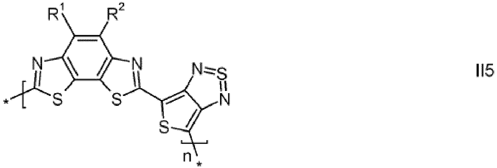
- Preferred polymers of formula II are selected from the group consisting of the following formulae: wherein R 1 , R 2 , Ar 1 , Ar 2 , Ar 3 and n have the meanings given above and below, and wherein Ar 1 , Ar 2 and Ar 3 do not denote a single bond.
- Polymers of the invention are selected from formulae II and IIA-IID from the group consisting of the following formulae: wherein R 1 , R 2 , R 3 , R 6 and n have the meanings as given in formula I and II or one of the preferred meanings as given above and below, and R 7 and R 8 have independently of each other one of the meanings of R 3 or its preferred meanings as given above and below.
- Preferred polymers of formula IIa are selected of the formula R 4 -chain-R 5 wherein "chain” is a polymer chain selected from above formulae IIA-IID and 111-15, and R 4 and R 5 have one of the meanings given in formula IIa or one of the preferred meanings given above and below.
- the polymers of the present invention can be synthesized according to or in analogy to methods that are known to the skilled person and are described in the literature. Other methods of preparation can be taken from the examples. For example, they can be suitably prepared by aryl-aryl coupling reactions, such as Yamamoto coupling, Suzuki coupling, Stille coupling, Sonogashira coupling, Heck coupling or Buchwald coupling. Suzuki coupling and Yamamoto coupling are especially preferred.
- the monomers which are polymerised to form the repeat units of the polymers can be prepared according to methods which are known to the person skilled in the art.
- polymers are prepared from monomers of formula Ia or its preferred embodiments as described above and below.
- Suitable and preferred comonomers are those of the formula R 4 -Ar 3 -R 5 wherein R 4 and R 5 have one of the meanings of formula IIa or one of the preferred meanings given above and below, and Ar 3 has one of the meanings of formula IIa or of Ar in formula IIa, or one of the preferred meanings given above and below.
- Preferred methods for polymerisation are those leading to C-C-coupling or C-N-coupling, like Suzuki polymerisation, as described for example in WO 00/53656, Yamamoto polymerisation, as described in for example in T. Yamamoto et al., Progress in Polymer Science 1993, 17, 1153-1205 or in WO 2004/022626 A1 , and Stille coupling.
- monomers as described above having two reactive halide groups R 4 and R 5 is preferably used.
- a monomer as described above is used wherein at least one reactive group R 4 or R 5 is a boronic acid or boronic acid derivative group.
- Suzuki polymerisation may be used to prepare homopolymers as well as statistical, alternating and block random copolymers.
- Statistical or block copolymers can be prepared for example from the above monomers of formula Ia wherein one of the reactive groups R 4 and R 5 is halogen and the other reactive group is a boronic acid or boronic acid derivative group.
- the synthesis of statistical, alternating and block copolymers is described in detail for example in WO 03/048225 A2 or WO 2005/014688 A2 .
- Suzuki polymerisation employs a Pd(0) complex or a Pd(II) salt.
- Preferred Pd(0) complexes are those bearing at least one phosphine ligand such as Pd(Ph 3 P) 4 .
- Another preferred phosphine ligand is tris( ortho- tolyl)phosphine, i.e. Pd(o-Tol) 4 .
- Preferred Pd(II) salts include palladium acetate, i.e. Pd(OAc) 2 .
- Suzuki polymerisation is performed in the presence of a base, for example sodium carbonate, potassium phosphate or an organic base such as tetraethylammonium carbonate.
- Yamamoto polymerisation employs a Ni(0) complex, for example bis(1,5-cyclooctadienyl) nickel(0).
- leaving groups of formula -O-SO 2 Z 1 can be used wherein Z 1 is as described above.
- Particular examples of such leaving groups are tosylate, mesylate and triflate.
- the polymers according to the present invention can also be used in mixtures or polymer blends, for example together with monomeric compounds or together with other polymers having charge-transport, semiconducting, electrically conducting, photoconducting and/or light emitting semiconducting properties, or for example with polymers having hole blocking or electron blocking properties for use as interlayers or charge blocking layers in OLED devices.
- another aspect of the invention relates to a polymer blend comprising one or more polymers according to the present invention and one or more further polymers having one or more of the above-mentioned properties.
- These blends can be prepared by conventional methods that are described in prior art and known to the skilled person. Typically the polymers are mixed with each other or dissolved in suitable solvents and the solutions combined.
- Another aspect of the invention relates to a formulation comprising one or more polymers, mixtures or polmyer blends as described above and below and one or more organic solvents.
- Preferred solvents are aliphatic hydrocarbons, chlorinated hydrocarbons, aromatic hydrocarbons, ketones, ethers and mixtures thereof. Additional solvents which can be used include 1,2,4-trimethylbenzene, 1,2,3,4-tetramethyl benzene, pentylbenzene, mesitylene, cumene, cymene, cyclohexylbenzene, diethylbenzene, tetralin, decalin, 2,6-lutidine, 2-fluoro-m-xylene, 3-fluoro-o-xylene, 2-chlorobenzotrifluoride, dimethylformamide, 2-chloro-6fluorotoluene, 2-fluoroanisole, anisole, 2,3-dimethylpyrazine, 4-fluoroanisole, 3-fluoroanisole, 3-trifluoro-methylanisole, 2-methylanisole, phenetol, 4-methylanisole, 3-methylanisole, 4-fluoro-3-methylanisole
- solvents include, without limitation, dichloromethane, trichloromethane, monochlorobenzene, o-dichlorobenzene, tetrahydrofuran, anisole, morpholine, toluene, o-xylene, m-xylene, p-xylene, 1,4-dioxane, acetone, methylethylketone, 1,2-dichloroethane, 1,1,1-trichloroethane, 1,1,2,2-tetrachloroethane, ethyl acetate, n-butyl acetate, dimethylformamide, dimethylacetamide, dimethylsulfoxide, tetraline, decaline, indane, methyl benzoate, ethyl benzoate, mesitylene and/or mixtures thereof.
- the concentration of the polymers in the solution is preferably 0.1 to 10% by weight, more preferably 0.5 to 5% by weight.
- the solution also comprises one or more binders to adjust the rheological properties, as described for example in WO 2005/055248 A1 .
- solutions are evaluated as one of the following categories: complete solution, borderline solution or insoluble.
- the contour line is drawn to outline the solubility parameter-hydrogen bonding limits dividing solubility and insolubility.
- Solvent blends may also be used and can be identified as described in " Solvents, W.H.Ellis, Federation of Societies for Coatings Technology, p9-10, 1986 ". Such a procedure may lead to a blend of 'non' solvents that will dissolve both the polymers of the present invention, although it is desirable to have at least one true solvent in a blend.
- the polymers according to the present invention can also be used in patterned OSC layers in the devices as described above and below. For applications in modern microelectronics it is generally desirable to generate small structures or patterns to reduce cost (more devices/unit area), and power consumption. Patterning of thin layers comprising a polymer according to the present invention can be carried out for example by photolithography, electron beam lithography or laser patterning.
- the polymers, polymer blends or formulations of the present invention may be deposited by any suitable method.
- Liquid coating of devices is more desirable than vacuum deposition techniques.
- Solution deposition methods are especially preferred.
- the formulations of the present invention enable the use of a number of liquid coating techniques.
- Preferred deposition techniques include, without limitation, dip coating, spin coating, ink jet printing, letter-press printing, screen printing, doctor blade coating, roller printing, reverse-roller printing, offset lithography printing, flexographic printing, web printing, spray coating, brush coating or pad printing.
- Ink-jet printing is particularly preferred as it allows high resolution layers and devices to be prepared.
- Selected formulations of the present invention may be applied to prefabricated device substrates by ink jet printing or microdispensing.
- industrial piezoelectric print heads such as but not limited to those supplied by Aprion, Hitachi-Koki, InkJet Technology, On Target Technology, Picojet, Spectra, Trident, Xaar may be used to apply the organic semiconductor layer to a substrate.
- semi-industrial heads such as those manufactured by Brother, Epson, Konica, Seiko Instruments Toshiba TEC or single nozzle microdispensers such as those produced by Microdrop and Microfab may be used.
- the polymers In order to be applied by ink jet printing or microdispensing, the polymers should be first dissolved in a suitable solvent. Solvents must fulfil the requirements stated above and must not have any detrimental effect on the chosen print head. Additionally, solvents should have boiling points >100°C, preferably >140°C and more preferably >150°C in order to prevent operability problems caused by the solution drying out inside the print head.
- suitable solvents include substituted and non-substituted xylene derivatives, di-C 1 - 2 -alkyl formamide, substituted and non-substituted anisoles and other phenol-ether derivatives, substituted heterocycles such as substituted pyridines, pyrazines, pyrimidines, pyrrolidinones, substituted and non-substituted N , N -di-C 1-2 -alkylanilines and other fluorinated or chlorinated aromatics.
- a preferred solvent for depositing a polymer according to the present invention by ink jet printing comprises a benzene derivative which has a benzene ring substituted by one or more substituents wherein the total number of carbon atoms among the one or more substituents is at least three.
- the benzene derivative may be substituted with a propyl group or three methyl groups, in either case there being at least three carbon atoms in total.
- Such a solvent enables an ink jet fluid to be formed comprising the solvent with the polymer, which reduces or prevents clogging of the jets and separation of the components during spraying.
- the solvent(s) may include those selected from the following list of examples: dodecylbenzene, 1-methyl-4-tert-butylbenzene, terpineol limonene, isodurene, terpinolene, cymene, diethylbenzene.
- the solvent may be a solvent mixture, that is a combination of two or more solvents, each solvent preferably having a boiling point >100°C, more preferably >140°C. Such solvent(s) also enhance film formation in the layer deposited and reduce defects in the layer.
- the ink jet fluid (that is mixture of solvent, binder and semiconducting compound) preferably has a viscosity at 20°C of 1-100 mPas, more preferably 1-50 mPas and most preferably 1-30 mPas.
- the polymers or formulations according to the present invention can additionally comprise one or more further components or additives selected for for example from surface-active compounds, lubricating agents, wetting agents, dispersing agents, hydrophobing agents, adhesive agents, flow improvers, defoaming agents, deaerators, diluents which may be reactive or non-reactive, auxiliaries, colourants, dyes or pigments, sensitizers, stabilizers, nanoparticles or inhibitors.
- surface-active compounds lubricating agents, wetting agents, dispersing agents, hydrophobing agents, adhesive agents, flow improvers, defoaming agents, deaerators, diluents which may be reactive or non-reactive, auxiliaries, colourants, dyes or pigments, sensitizers, stabilizers, nanoparticles or inhibitors.
- the polymers according to the present invention are useful as charge transport, semiconducting, electrically conducting, photoconducting or light mitting materials in optical, electrooptical, electronic, electroluminescent or photoluminescent components or devices.
- the polymers of the present invention are typically applied as thin layers or films.
- the present invention also provides the use of the semiconducting polymer, polymer blend, formulation or layer in an electronic device.
- the formulation may be used as a high mobility semiconducting material in various devices and apparatus.
- the formulation may be used, for example, in the form of a semiconducting layer or film.
- the present invention provides a semiconducting layer for use in an electronic device, the layer comprising a polymer, polymer blend or formulation according to the invention.
- the layer or film may be less than about 30 microns.
- the thickness may be less than about 1 micron thick.
- the layer may be deposited, for example on a part of an electronic device, by any of the aforementioned solution coating or printing techniques.
- the invention additionally provides an electronic device comprising a polymer, polymer blend, formulation or organic semiconducting layer according to the present invention.
- Especially preferred devices are OFETs, TFTs, ICs, logic circuits, capacitors, RFID tags, OLEDs, OLETs, OPEDs, OPVs, solar cells, laser diodes, photoconductors, photodetectors, electrophotographic devices, electrophotographic recording devices, organic memory devices, sensor devices, charge injection layers, Schottky diodes, planarising layers, antistatic films, conducting substrates and conducting patterns.
- Especially preferred electronic device are OFETs, OLEDs and OPV devices, in particular bulk heterojunction (BHJ) OPV devices.
- the active semiconductor channel between the drain and source may comprise the layer of the invention.
- the charge (hole or electron) injection or transport layer may comprise the layer of the invention.
- the polymer according to the present invention is preferably used in a formulation that comprises or contains, more preferably consists essentially of, very preferably exclusively of, a p-type (electron donor) semiconductor and an n-type (electron acceptor) semiconductor.
- the p-type semiconductor is constituted by a polymer according to the present invention.
- the n-type semiconductor can be an inorganic material such as zinc oxide or cadmium selenide, or an organic material such as a fullerene derivate, for example (6,6)-phenyl-butyric acid methyl ester derivatized methano C 60 fullerene, also known as "PCBM” or "C 60 PCBM", as disclosed for example in G. Yu, J.
- a preferred material of this type is a blend or mixture of a polymer according to the present invention with a C 60 or C 70 fullerene or modified fullerene like PCBM.
- the ratio polymer:fullerene is from 2:1 to 1:2 by weight, more preferably from 1.2:1 to 1:1.2 by weight, most preferably 1:1 by weight.
- an optional annealing step may be necessary to optimize blend morpohology and consequently OPV device performance.
- the OPV device can for example be of any type known from the literature [see e.g. Waldauf et al., Appl. Phys. Lett. 89, 233517 (2006 )].
- a first preferred OPV device comprises:
- a second preferred OPV device is an inverted OPV device and comprises:
- the p-type and n-type semiconductor materials are preferably selected from the materials, like the polymer/fullerene systems, as described above. If the bilayer is a blend an optional annealing step may be necessary to optimize device performance.
- the compound, formulation and layer of the present invention are also suitable for use in an OFET as the semiconducting channel.
- the invention also provides an OFET comprising a gate electrode, an insulating (or gate insulator) layer, a source electrode, a drain electrode and an organic semiconducting channel connecting the source and drain electrodes, wherein the organic semiconducting channel comprises a polymer, polymer blend, formulation or organic semiconducting layer according to the present invention.
- an OFET comprising a gate electrode, an insulating (or gate insulator) layer, a source electrode, a drain electrode and an organic semiconducting channel connecting the source and drain electrodes, wherein the organic semiconducting channel comprises a polymer, polymer blend, formulation or organic semiconducting layer according to the present invention.
- Other features of the OFET are well known to those skilled in the art.
- OFETs where an OSC material is arranged as a thin film between a gate dielectric and a drain and a source electrode are generally known, and are described for example in US 5,892,244 , US 5,998,804 , US 6,723,394 and in the references cited in the background section. Due to the advantages, like low cost production using the solubility properties of the compounds according to the invention and thus the processibility of large surfaces, preferred applications of these FETs are such as integrated circuitry, TFT displays and security applications.
- the gate, source and drain electrodes and the insulating and semiconducting layer in the OFET device may be arranged in any sequence, provided that the source and drain electrode are separated from the gate electrode by the insulating layer, the gate electrode and the semiconductor layer both contact the insulating layer, and the source electrode and the drain electrode both contact the semiconducting layer.
- An OFET device preferably comprises:
- the OFET device can be a top gate device or a bottom gate device. Suitable structures and manufacturing methods of an OFET device are known to the skilled in the art and are described in the literature, for example in US 2007/0102696 A1 .
- the gate insulator layer preferably comprises a fluoropolymer, like e.g. the commercially available Cytop 809M® or Cytop 107M® (from Asahi Glass).
- a fluoropolymer like e.g. the commercially available Cytop 809M® or Cytop 107M® (from Asahi Glass).
- the gate insulator layer is deposited, e.g. by spin-coating, doctor blading, wire bar coating, spray or dip coating or other known methods, from a formulation comprising an insulator material and one or more solvents with one or more fluoro atoms (fluorosolvents), preferably a perfluorosolvent.
- fluorosolvents fluoro atoms
- a suitable perfluorosolvent is e.g. FC75® (available from Acros, catalogue number 12380).
- fluoropolymers and fluorosolvents are known in prior art, like for example the perfluoropolymers Teflon AF® 1600 or 2400 (from DuPont) or Fluoropel® (from Cytonix) or the perfluorosolvent FC 43® (Acros, No. 12377).
- organic dielectric materials having a low permittivity (or dielectric contant) from 1.0 to 5.0, very preferably from 1.8 to 4.0 (“low k materials”), as disclosed for example in US 2007/0102696 A1 or US 7,095,044 .
- OFETs and other devices with semiconducting materials according to the present invention can be used for RFID tags or security markings to authenticate and prevent counterfeiting of documents of value like banknotes, credit cards or ID cards, national ID documents, licenses or any product with monetry value, like stamps, tickets, shares, cheques etc..
- the materials according to the invention can be used in OLEDs, e.g. as the active display material in a flat panel display applications, or as backlight of a flat panel display like e.g. a liquid crystal display.
- OLEDs are realized using multilayer structures.
- An emission layer is generally sandwiched between one or more electron-transport and/ or hole-transport layers.
- the inventive compounds, materials and films may be employed in one or more of the charge transport layers and/ or in the emission layer, corresponding to their electrical and/ or optical properties.
- the compounds, materials and films according to the invention show electroluminescent properties themselves or comprise electroluminescent groups or compounds.
- the selection, characterization as well as the processing of suitable monomeric, oligomeric and polymeric compounds or materials for the use in OLEDs is generally known by a person skilled in the art, see, e.g., Meerholz, Synthetic Materials, 111-112, 2000, 31-34 , Alcala, J. Appl. Phys., 88, 2000, 7124-7128 and the literature cited therein.
- the materials according to this invention may be employed as materials of light sources, e.g. in display devices, as described in EP 0 889 350 A1 or by C. Weder et al., Science, 279, 1998, 835-837 .
- a further aspect of the invention relates to both the oxidised and reduced form of the compounds according to this invention. Either loss or gain of electrons results in formation of a highly delocalised ionic form, which is of high conductivity. This can occur on exposure to common dopants. Suitable dopants and methods of doping are known to those skilled in the art, e.g. from EP 0 528 662 , US 5,198,153 or WO 96/21659 .
- the doping process typically implies treatment of the semiconductor material with an oxidating or reducing agent in a redox reaction to form delocalised ionic centres in the material, with the corresponding counterions derived from the applied dopants.
- Suitable doping methods comprise for example exposure to a doping vapor in the atmospheric pressure or at a reduced pressure, electrochemical doping in a solution containing a dopant, bringing a dopant into contact with the semiconductor material to be thermally diffused, and ion-implantantion of the dopant into the semiconductor material.
- suitable dopants are for example halogens (e.g., I 2 , Cl 2 , Br2, ICI, ICl 3 , IBr and IF), Lewis acids (e.g., PF 5 , AsF 5 , SbFs, BF 3 , BCl 3 , SbCl 5 , BBr 3 and SO 3 ), protonic acids, organic acids, or amino acids (e.g., HF, HCI, HNO 3 , H 2 SO 4 , HClO 4 , FSO 3 H and ClSO 3 H), transition metal compounds (e.g., FeCl 3 , FeOCI, Fe(ClO 4 ) 3 , Fe(4-CH 3 CsH 4 SO 3 ) 3 , TiCl 4 , ZrCl 4 , HfCl 4 , NbFs, NbCl 5 , TaCl 5 , MoF 5 , MoCl 5 , WF 5 , WCl 6
- Lewis acids e.
- examples of dopants are cations (e.g., H + , Li + , Na + , K + , Rb + and Cs + ), alkali metals (e.g., Li, Na, K, Rb, and Cs), alkaline-earth metals (e.g., Ca, Sr, and Ba), O 2 , XeOF 4 , (NO 2 + ) (SbF 6 - ), (NO 2 + ) (SbCl 6 - ), (NO 2 + ) (BF 4 - ), AgClO 4 , H 2 IrCl 6 , La(NO 3 ) 3 6H 2 O, FSO 2 OOSO 2 F, Eu, acetylcholine, R 4 N + , (R is an alkyl group), R 4 P + (R is an alkyl group), R 6 As + (R is an alkyl group), and R 3 S + (R is an alkyl group).
- dopants are cations (
- the conducting form of the compounds of the present invention can be used as an organic "metal" in applications including, but not limited to, charge injection layers and ITO planarising layers in OLED applications, films for flat panel displays and touch screens, antistatic films, printed conductive substrates, patterns or tracts in electronic applications such as printed circuit boards and condensers.
- the compounds and formulations according to the present invention amy also be suitable for use in organic plasmon-emitting diodes (OPEDs), as described for example in Koller et al., Nature Photonics 2008 (published online September 28, 2008 ).
- OPEDs organic plasmon-emitting diodes
- the materials according to the present invention can be used alone or together with other materials in or as alignment layers in LCD or OLED devices, as described for example in US 2003/0021913 .
- the use of charge transport compounds according to the present invention can increase the electrical conductivity of the alignment layer. When used in an LCD, this increased electrical conductivity can reduce adverse residual dc effects in the switchable LCD cell and suppress image sticking or, for example in ferroelectric LCDs, reduce the residual charge produced by the switching of the spontaneous polarisation charge of the ferroelectric LCs. When used in an OLED device comprising a light emitting material provided onto the alignment layer, this increased electrical conductivity can enhance the electroluminescence of the light emitting material.
- the compounds or materials according to the present invention having mesogenic or liquid crystalline properties can form oriented anisotropic films as described above, which are especially useful as alignment layers to induce or enhance alignment in a liquid crystal medium provided onto said anisotropic film.
- the materials according to the present invention may also be combined with photoisomerisable compounds and/or chromophores for use in or as photoalignment layers, as described in US 2003/0021913 .
- the materials according to the present invention can be employed as chemical sensors or materials for detecting and discriminating DNA sequences.
- Such uses are described for example in L. Chen, D. W. McBranch, H. Wang, R. Helgeson, F. Wudl and D. G. Whitten, Proc. Natl. Acad. Sci. U.S.A. 1999, 96, 12287 ; D. Wang, X. Gong, P. S. Heeger, F. Rininsland, G. C. Bazan and A. J. Heeger, Proc. Natl. Acad. Sci. U.S.A.
- reaction mixture is diluted with ethyl acetate (500 cm 3 ) and washed with aqueous sodium hydrogen carbonate solution, brine and dried over anhydrous magnesium sulfate, filtered and the solvent removed in vacuo to give a dark brown oil.
- the residue is purified by column chromatography (40-60 petrol to 1:1 40-60 petrol:dichloromethane) to give 5-iodo-2-triisopropylsilanyl-thiazole as a very pale yellow solid (65 g, 78%).
- 1 H NMR 300 MHz, CDCl 3 ) 1.10 - 1.16 (18H, m, CH 3 ), 1.34 - 1.48 (3H, m, CH), 8.10 (1H, s).
- the mixture is allowed to cool and poured into aqueous hydrochloric acid (2 M, 50 cm 3 ) and the organics extracted with dichloromethane (2 x 50 cm 3 ).
- the combined extracts dried over anhydrous magnesium sulfate, filtered and the solvent removed in vacuo.
- the crude is purified by column chromatography (40-60 petrol to dichloromethane).
- the purified material is deprotected by stirring with tetrabutylammonium fluoride trihydrate (1.5 g, 4.8 mmol) and tetrahydrofuran (40 cm 3 ) at 70 °C for 1 hour.
- the mixture is allowed to cool, water (50 cm 3 ) added and the organics extracted with dichloromethane (2 x 100 cm 3 ).
- the mixture is then heated at 170 °C in a microwave reactor (Initiator, Biotage AB) for 30 minutes.
- the mixture is allowed to cool and poured into stirring methanol (100 cm 3 ) and the precipitate stirred for 30 minutes.
- the solid is then collected by filtration, washed with methanol (100 cm 3 ) to give a black solid.
- the crude polymer is washed via Soxhlet extraction with acetone, methanol, 40-60 petrol and chloroform.
- the chloroform extract is precipitated into stirred methanol (400 cm 3 ).
Landscapes
- Chemical & Material Sciences (AREA)
- Polymers & Plastics (AREA)
- Health & Medical Sciences (AREA)
- Chemical Kinetics & Catalysis (AREA)
- Medicinal Chemistry (AREA)
- Organic Chemistry (AREA)
- Materials Engineering (AREA)
- Engineering & Computer Science (AREA)
- Physics & Mathematics (AREA)
- Electromagnetism (AREA)
- Polyoxymethylene Polymers And Polymers With Carbon-To-Carbon Bonds (AREA)
- Electroluminescent Light Sources (AREA)
- Press Drives And Press Lines (AREA)
- Punching Or Piercing (AREA)
Claims (9)
- Polymère qui est sélectionné dans le groupe consistant en les sous-formules suivantes :




 dans lesquelles R1 et/ou R2 sont sélectionnés parmi les groupes suivants :a) le groupe consistant en un alkyle ou alcoxy primaire ayant 1 à 30 atomes C, un alkyle ou alcoxy secondaire ayant 3 à 30 atomes C, et un alkyle ou alcoxy tertiaire ayant 4 à 30 atomes C, dans lequel, dans tous ces groupes, un ou plusieurs atomes H sont facultativement remplacés par F,b) le groupe consistant en -C(O)-R6, -C(O)-O-R6, -O-C(O)-R6,dans lesquels R6 est un alkyle linéaire, ramifié ou cyclique ayant 1 à 30 atomes C, dans lesquels un ou plusieurs atomes C non adjacents sont facultativement remplacés par - O-, -S-, -C(O)-, -C(O)-O-, -OC(O)-, -O-C(O)-O-, -CR0=CR00- ou -C≡C- et dans lesquels un ou plusieurs atomes H sont facultativement remplacés par F, Cl, Br, I ou CN,c) le groupe consistant en un aryle, un aryloxy, un hétéroaryle et un hétéroaryloxy qui sont facultativement alkylés ou alcoxylés et présentent 4 à 30 atomes de cycle,R3 est, à chaque occurrence identique ou différente, F, Br, Cl, -CN, -NC, -NCO, - NCS, -OCN, -SCN, -C(O)NR0R00, -C(O)X0, -C(O)R0, -NH2, -NR0R00, -SH, -SR0, -SO3H, -SO2R0, - OH, -NO2, -CF3, -SF5, un silyle facultativement substitué, un carbyle ou un hydrocarbyle ayant 1 à 40 atomes C qui est facultativement substitué et comprend facultativement un ou plusieurs hétéroatomes, ou P-Sp-,R0 et R00 sont indépendamment l'un de l'autre H ou un carbyle ou hydrocarbyle en C1-40 facultativement substitué,P est un groupe polymérisable ou réticulable,Sp est un groupe espaceur ou une liaison simple,X0 est un halogène,R6 est un alkyle linéaire, ramifié ou cyclique ayant 1 à 30 atomes C, dans lequel un ou plusieurs atomes C non adjacents sont facultativement remplacés par - O-, -S-, - C(O)-, -C(O)-O-, -O-C(O)-, -O-C(O)-O-, -CR0=CR00- ou -C≡C- et dans lequel un ou plusieurs atomes H sont facultativement remplacés par F, Cl, Br, I ou CN ;n est un nombre entier > 1et R4, R7 et R8 possèdent indépendamment les uns des autres l'une des significations de R3.
 - Polymère selon la revendication 1, caractérisé en ce que R3 est F, Cl, Br, I, CN, R6, - C(O)-R6, -C(O)-O-R6, ou -O-C(O)-R6, ou R3 est un aryle, un aryloxy, un hétéroaryle ou un hétéroaryloxy, chacun présentant 4 à 30 atomes de cycle et étant non substitué ou substitué avec un ou plusieurs atomes d'halogène ou avec un ou plusieurs groupes R6, - C(O)-R6, -C(O)-O-R6, ou -O-C(O)-R6 dans lesquels R6 est tel que défini dans la revendication 1.
- Polymère selon la revendication 1 ou 2, caractérisé en ce que R0 et R00 sont sélectionnés parmi H ou un alkyle en C1 à C10.
- Mélange comprenant un ou plusieurs polymères selon une ou plusieurs des revendications 1 à 3 et un ou plusieurs composés ou polymères présentant des propriétés de semiconducteur, de transport de charges, de transport de trous/d'électrons, de blocage de trous/d'électrons, d'électroconduction, de photoconduction ou d'émission de lumière.
- Formulation comprenant un ou plusieurs polymères ou mélanges selon une ou plusieurs des revendications 1 à 4, et un ou plusieurs solvants, de préférence sélectionnés parmi les solvants organiques.
- Utilisation d'un polymère, d'un mélange ou d'une formulation selon une ou plusieurs des revendications 1 à 5 comme matériau de transport de charges, semiconducteur, électroconducteur, photoconducteur ou émetteur de lumière dans des composants ou dispositifs optiques, électrooptiques, électroniques, électroluminescents ou photoluminescents.
- Composant ou dispositif optique, électrooptique ou électronique comprenant un ou plusieurs polymères, mélanges ou formulations selon une ou plusieurs des revendications 1 à 5.
- Composant ou dispositif selon la revendication 7, qui est sélectionné dans le groupe consistant en les transistors organiques à effet de champ (OFET), les transistors à couches minces (TFT), les circuits intégrés (IC), les circuits logiques, les condensateurs, les étiquettes, dispositifs ou composants d'identification par radiofréquence (RFID), les diodes électroluminescentes organiques (OLED), les transistors électroluminescents organiques (OLET), les affichages à écran plat, les rétroéclairages d'affichages, les dispositifs photovoltaïques organiques (OPV), les cellules solaires, les diodes laser, les photoconducteurs, les photodétecteurs, les dispositifs électrophotographiques, les dispositifs d'enregistrement électrophotographique, les dispositifs organiques de mémoire, les dispositifs de détection, les couches d'injection de charges, les couches ou couches intermédiaires de transport de charges dans les diodes électroluminescentes polymères (PLEDs), les diodes Schottky, les couches de planarisation, les films antistatiques, les membranes à électrolyte polymère (PEM), les substrats conducteurs, les motifs conducteurs, les matériaux d'électrodes dans les batteries, les couches d'alignement, les biocapteurs, les biopuces, les marquages de sécurité, les dispositifs de sécurité, et les composants ou dispositifs de détection et de discrimination de séquences d'ADN.
- Composant ou dispositif selon la revendication 7 ou 8, qui est un OFET ou un dispositif OPV à hétérojonction en masse.
Priority Applications (1)
| Application Number | Priority Date | Filing Date | Title |
|---|---|---|---|
| EP11758412.8A EP2630179B1 (fr) | 2010-10-20 | 2011-09-21 | Polymères conjugués |
Applications Claiming Priority (3)
| Application Number | Priority Date | Filing Date | Title |
|---|---|---|---|
| EP10013798 | 2010-10-20 | ||
| PCT/EP2011/004730 WO2012052099A1 (fr) | 2010-10-20 | 2011-09-21 | Polymères conjugués |
| EP11758412.8A EP2630179B1 (fr) | 2010-10-20 | 2011-09-21 | Polymères conjugués |
Publications (2)
| Publication Number | Publication Date |
|---|---|
| EP2630179A1 EP2630179A1 (fr) | 2013-08-28 |
| EP2630179B1 true EP2630179B1 (fr) | 2021-04-14 |
Family
ID=44658712
Family Applications (1)
| Application Number | Title | Priority Date | Filing Date |
|---|---|---|---|
| EP11758412.8A Active EP2630179B1 (fr) | 2010-10-20 | 2011-09-21 | Polymères conjugués |
Country Status (12)
| Country | Link |
|---|---|
| US (1) | US9559303B2 (fr) |
| EP (1) | EP2630179B1 (fr) |
| JP (1) | JP5912122B2 (fr) |
| KR (1) | KR101854942B1 (fr) |
| CN (1) | CN103168063B (fr) |
| CA (1) | CA2754874C (fr) |
| DE (1) | DE112011103524T5 (fr) |
| GB (1) | GB2497879A (fr) |
| RU (1) | RU2013122682A (fr) |
| SG (1) | SG189378A1 (fr) |
| TW (1) | TWI519564B (fr) |
| WO (1) | WO2012052099A1 (fr) |
Families Citing this family (3)
| Publication number | Priority date | Publication date | Assignee | Title |
|---|---|---|---|---|
| WO2015166360A1 (fr) | 2014-04-29 | 2015-11-05 | Sabic Global Technologies B.V. | Synthèse de nouvelles petites molécules/oligomères à haute conductivité et à forte absorption pour application opto-électronique |
| JP7172655B2 (ja) | 2019-01-25 | 2022-11-16 | 株式会社リコー | 光電変換素子、機器、及び電源モジュール |
| JP7834322B2 (ja) * | 2021-08-23 | 2026-03-24 | 国立大学法人広島大学 | 共役系重合体、共役系化合物、これを用いた電子供与性有機材料、光起電力素子用材料および光起電力素子 |
Family Cites Families (23)
| Publication number | Priority date | Publication date | Assignee | Title |
|---|---|---|---|---|
| US4522745A (en) * | 1982-11-17 | 1985-06-11 | Chevron Research Company | Fused 5,6,5-membered heterocyclic electroactive polymers |
| US5892244A (en) | 1989-01-10 | 1999-04-06 | Mitsubishi Denki Kabushiki Kaisha | Field effect transistor including πconjugate polymer and liquid crystal display including the field effect transistor |
| US5198153A (en) | 1989-05-26 | 1993-03-30 | International Business Machines Corporation | Electrically conductive polymeric |
| JP3224829B2 (ja) | 1991-08-15 | 2001-11-05 | 株式会社東芝 | 有機電界効果型素子 |
| WO1996021659A1 (fr) | 1995-01-10 | 1996-07-18 | University Of Technology, Sydney | Semi-conducteur organique |
| EP0889350A1 (fr) | 1997-07-03 | 1999-01-07 | ETHZ Institut für Polymere | Dispositifs d'affichage photoluminescents |
| US5998804A (en) | 1997-07-03 | 1999-12-07 | Hna Holdings, Inc. | Transistors incorporating substrates comprising liquid crystal polymers |
| JP3310658B1 (ja) | 1999-03-05 | 2002-08-05 | ケンブリッジ ディスプレイ テクノロジー リミテッド | 高分子の合成方法 |
| WO2000079617A1 (fr) | 1999-06-21 | 2000-12-28 | Cambridge University Technical Services Limited | Polymeres alignes pour tft organique |
| GB0028867D0 (en) | 2000-11-28 | 2001-01-10 | Avecia Ltd | Field effect translators,methods for the manufacture thereof and materials therefor |
| EP1366046B1 (fr) | 2001-01-24 | 2006-10-18 | Cambridge Display Technology Limited | Monomere destine a la preparation d'un polymere intervenant dans des appareils optiques |
| US20030021913A1 (en) | 2001-07-03 | 2003-01-30 | O'neill Mary | Liquid crystal alignment layer |
| DE10159946A1 (de) | 2001-12-06 | 2003-06-18 | Covion Organic Semiconductors | Prozess zur Herstellung von Aryl-Aryl gekoppelten Verbindungen |
| US6723934B2 (en) | 2002-03-04 | 2004-04-20 | Marybeth Enright | Method and apparatus for assisting left-handed manipulation of a vehicle ignition switch |
| DE10241814A1 (de) | 2002-09-06 | 2004-03-25 | Covion Organic Semiconductors Gmbh | Prozeß zur Herstellung von Aryl-Aryl gekoppelten Verbindungen |
| DE10337077A1 (de) | 2003-08-12 | 2005-03-10 | Covion Organic Semiconductors | Konjugierte Copolymere, deren Darstellung und Verwendung |
| EP1783781A3 (fr) | 2003-11-28 | 2007-10-03 | Merck Patent GmbH | Améliorations de et associées aux couches de semi-conducteur organique |
| US7772485B2 (en) * | 2005-07-14 | 2010-08-10 | Konarka Technologies, Inc. | Polymers with low band gaps and high charge mobility |
| EP2192123B1 (fr) | 2006-03-10 | 2012-11-21 | Sumitomo Chemical Company, Limited | Composé à tricycles fusionnés utiles dans les dispositifs à film en couche mince organique, par exemple les transistors |
| US8008424B2 (en) | 2006-10-11 | 2011-08-30 | Konarka Technologies, Inc. | Photovoltaic cell with thiazole-containing polymer |
| TW201002722A (en) * | 2008-01-22 | 2010-01-16 | Ricoh Co Ltd | Benzobisthiazole compound, benzobisthiazole polymer, organic film including the compound or polymer and transistor including the organic film |
| US20110006287A1 (en) | 2009-07-10 | 2011-01-13 | Wei You | Polymers with tunable band gaps for photonic and electronic applications |
| WO2011156478A2 (fr) * | 2010-06-08 | 2011-12-15 | The University Of North Carolina At Chapel Hill | Polymères, dont les largeurs de bande interdite sont accordables, et qui sont destinés à des applications photoniques et électroniques |
-
2011
- 2011-09-21 RU RU2013122682/04A patent/RU2013122682A/ru not_active Application Discontinuation
- 2011-09-21 US US13/879,249 patent/US9559303B2/en active Active
- 2011-09-21 SG SG2013027669A patent/SG189378A1/en unknown
- 2011-09-21 DE DE112011103524T patent/DE112011103524T5/de not_active Withdrawn
- 2011-09-21 CN CN201180050205.5A patent/CN103168063B/zh not_active Expired - Fee Related
- 2011-09-21 KR KR1020137012774A patent/KR101854942B1/ko not_active Expired - Fee Related
- 2011-09-21 GB GB1304913.5A patent/GB2497879A/en not_active Withdrawn
- 2011-09-21 WO PCT/EP2011/004730 patent/WO2012052099A1/fr not_active Ceased
- 2011-09-21 EP EP11758412.8A patent/EP2630179B1/fr active Active
- 2011-09-21 JP JP2013534182A patent/JP5912122B2/ja not_active Expired - Fee Related
- 2011-10-07 CA CA2754874A patent/CA2754874C/fr active Active
- 2011-10-19 TW TW100137977A patent/TWI519564B/zh not_active IP Right Cessation
Non-Patent Citations (1)
| Title |
|---|
| None * |
Also Published As
| Publication number | Publication date |
|---|---|
| CA2754874C (fr) | 2018-09-04 |
| TW201221542A (en) | 2012-06-01 |
| KR101854942B1 (ko) | 2018-05-04 |
| JP2013543031A (ja) | 2013-11-28 |
| CN103168063A (zh) | 2013-06-19 |
| SG189378A1 (en) | 2013-05-31 |
| WO2012052099A1 (fr) | 2012-04-26 |
| JP5912122B2 (ja) | 2016-04-27 |
| GB2497879A (en) | 2013-06-26 |
| DE112011103524T5 (de) | 2013-10-17 |
| US20130214208A1 (en) | 2013-08-22 |
| US9559303B2 (en) | 2017-01-31 |
| GB201304913D0 (en) | 2013-05-01 |
| RU2013122682A (ru) | 2014-11-27 |
| KR20130140017A (ko) | 2013-12-23 |
| EP2630179A1 (fr) | 2013-08-28 |
| CA2754874A1 (fr) | 2012-04-20 |
| TWI519564B (zh) | 2016-02-01 |
| CN103168063B (zh) | 2016-11-23 |
Similar Documents
| Publication | Publication Date | Title |
|---|---|---|
| US9287504B2 (en) | Semiconducting polymers | |
| US10155774B2 (en) | Semiconducting polymers | |
| US9837613B2 (en) | Conjugated polymers | |
| US9048433B2 (en) | Conjugated polymers | |
| EP2464627B1 (fr) | Polymères de phénanthro[1,10,9,8-c,d,e,f,g]carbazole et leur utilisation en tant que semi-conducteurs organiques | |
| US9212260B2 (en) | Polymers of 8,9-dihydrobenzo[def]carbazole and their use as organic semiconductors | |
| US9287505B2 (en) | Semiconducting polymers | |
| EP2904067A1 (fr) | Semi-conducteurs organiques | |
| US20140001411A1 (en) | Conjugated polymers | |
| US20140034880A1 (en) | Conjugated polymers | |
| EP2630179B1 (fr) | Polymères conjugués |
Legal Events
| Date | Code | Title | Description |
|---|---|---|---|
| PUAI | Public reference made under article 153(3) epc to a published international application that has entered the european phase |
Free format text: ORIGINAL CODE: 0009012 |
|
| 17P | Request for examination filed |
Effective date: 20130312 |
|
| AK | Designated contracting states |
Kind code of ref document: A1 Designated state(s): AL AT BE BG CH CY CZ DE DK EE ES FI FR GB GR HR HU IE IS IT LI LT LU LV MC MK MT NL NO PL PT RO RS SE SI SK SM TR |
|
| DAX | Request for extension of the european patent (deleted) | ||
| 17Q | First examination report despatched |
Effective date: 20140411 |
|
| STAA | Information on the status of an ep patent application or granted ep patent |
Free format text: STATUS: EXAMINATION IS IN PROGRESS |
|
| RAP1 | Party data changed (applicant data changed or rights of an application transferred) |
Owner name: RAYNERGY TEK INC. |
|
| GRAP | Despatch of communication of intention to grant a patent |
Free format text: ORIGINAL CODE: EPIDOSNIGR1 |
|
| STAA | Information on the status of an ep patent application or granted ep patent |
Free format text: STATUS: GRANT OF PATENT IS INTENDED |
|
| INTG | Intention to grant announced |
Effective date: 20201222 |
|
| GRAS | Grant fee paid |
Free format text: ORIGINAL CODE: EPIDOSNIGR3 |
|
| GRAA | (expected) grant |
Free format text: ORIGINAL CODE: 0009210 |
|
| STAA | Information on the status of an ep patent application or granted ep patent |
Free format text: STATUS: THE PATENT HAS BEEN GRANTED |
|
| AK | Designated contracting states |
Kind code of ref document: B1 Designated state(s): AL AT BE BG CH CY CZ DE DK EE ES FI FR GB GR HR HU IE IS IT LI LT LU LV MC MK MT NL NO PL PT RO RS SE SI SK SM TR |
|
| REG | Reference to a national code |
Ref country code: GB Ref legal event code: FG4D |
|
| REG | Reference to a national code |
Ref country code: CH Ref legal event code: EP |
|
| REG | Reference to a national code |
Ref country code: DE Ref legal event code: R096 Ref document number: 602011070688 Country of ref document: DE |
|
| REG | Reference to a national code |
Ref country code: IE Ref legal event code: FG4D |
|
| REG | Reference to a national code |
Ref country code: AT Ref legal event code: REF Ref document number: 1382338 Country of ref document: AT Kind code of ref document: T Effective date: 20210515 |
|
| REG | Reference to a national code |
Ref country code: LT Ref legal event code: MG9D |
|
| REG | Reference to a national code |
Ref country code: AT Ref legal event code: MK05 Ref document number: 1382338 Country of ref document: AT Kind code of ref document: T Effective date: 20210414 |
|
| REG | Reference to a national code |
Ref country code: NL Ref legal event code: MP Effective date: 20210414 |
|
| PG25 | Lapsed in a contracting state [announced via postgrant information from national office to epo] |
Ref country code: FI Free format text: LAPSE BECAUSE OF FAILURE TO SUBMIT A TRANSLATION OF THE DESCRIPTION OR TO PAY THE FEE WITHIN THE PRESCRIBED TIME-LIMIT Effective date: 20210414 Ref country code: NL Free format text: LAPSE BECAUSE OF FAILURE TO SUBMIT A TRANSLATION OF THE DESCRIPTION OR TO PAY THE FEE WITHIN THE PRESCRIBED TIME-LIMIT Effective date: 20210414 Ref country code: LT Free format text: LAPSE BECAUSE OF FAILURE TO SUBMIT A TRANSLATION OF THE DESCRIPTION OR TO PAY THE FEE WITHIN THE PRESCRIBED TIME-LIMIT Effective date: 20210414 Ref country code: HR Free format text: LAPSE BECAUSE OF FAILURE TO SUBMIT A TRANSLATION OF THE DESCRIPTION OR TO PAY THE FEE WITHIN THE PRESCRIBED TIME-LIMIT Effective date: 20210414 Ref country code: BG Free format text: LAPSE BECAUSE OF FAILURE TO SUBMIT A TRANSLATION OF THE DESCRIPTION OR TO PAY THE FEE WITHIN THE PRESCRIBED TIME-LIMIT Effective date: 20210714 Ref country code: AT Free format text: LAPSE BECAUSE OF FAILURE TO SUBMIT A TRANSLATION OF THE DESCRIPTION OR TO PAY THE FEE WITHIN THE PRESCRIBED TIME-LIMIT Effective date: 20210414 |
|
| PG25 | Lapsed in a contracting state [announced via postgrant information from national office to epo] |
Ref country code: IS Free format text: LAPSE BECAUSE OF FAILURE TO SUBMIT A TRANSLATION OF THE DESCRIPTION OR TO PAY THE FEE WITHIN THE PRESCRIBED TIME-LIMIT Effective date: 20210814 Ref country code: LV Free format text: LAPSE BECAUSE OF FAILURE TO SUBMIT A TRANSLATION OF THE DESCRIPTION OR TO PAY THE FEE WITHIN THE PRESCRIBED TIME-LIMIT Effective date: 20210414 Ref country code: GR Free format text: LAPSE BECAUSE OF FAILURE TO SUBMIT A TRANSLATION OF THE DESCRIPTION OR TO PAY THE FEE WITHIN THE PRESCRIBED TIME-LIMIT Effective date: 20210715 Ref country code: SE Free format text: LAPSE BECAUSE OF FAILURE TO SUBMIT A TRANSLATION OF THE DESCRIPTION OR TO PAY THE FEE WITHIN THE PRESCRIBED TIME-LIMIT Effective date: 20210414 Ref country code: RS Free format text: LAPSE BECAUSE OF FAILURE TO SUBMIT A TRANSLATION OF THE DESCRIPTION OR TO PAY THE FEE WITHIN THE PRESCRIBED TIME-LIMIT Effective date: 20210414 Ref country code: PT Free format text: LAPSE BECAUSE OF FAILURE TO SUBMIT A TRANSLATION OF THE DESCRIPTION OR TO PAY THE FEE WITHIN THE PRESCRIBED TIME-LIMIT Effective date: 20210816 Ref country code: PL Free format text: LAPSE BECAUSE OF FAILURE TO SUBMIT A TRANSLATION OF THE DESCRIPTION OR TO PAY THE FEE WITHIN THE PRESCRIBED TIME-LIMIT Effective date: 20210414 Ref country code: NO Free format text: LAPSE BECAUSE OF FAILURE TO SUBMIT A TRANSLATION OF THE DESCRIPTION OR TO PAY THE FEE WITHIN THE PRESCRIBED TIME-LIMIT Effective date: 20210714 Ref country code: ES Free format text: LAPSE BECAUSE OF FAILURE TO SUBMIT A TRANSLATION OF THE DESCRIPTION OR TO PAY THE FEE WITHIN THE PRESCRIBED TIME-LIMIT Effective date: 20210414 |
|
| REG | Reference to a national code |
Ref country code: DE Ref legal event code: R097 Ref document number: 602011070688 Country of ref document: DE |
|
| PG25 | Lapsed in a contracting state [announced via postgrant information from national office to epo] |
Ref country code: SM Free format text: LAPSE BECAUSE OF FAILURE TO SUBMIT A TRANSLATION OF THE DESCRIPTION OR TO PAY THE FEE WITHIN THE PRESCRIBED TIME-LIMIT Effective date: 20210414 Ref country code: SK Free format text: LAPSE BECAUSE OF FAILURE TO SUBMIT A TRANSLATION OF THE DESCRIPTION OR TO PAY THE FEE WITHIN THE PRESCRIBED TIME-LIMIT Effective date: 20210414 Ref country code: DK Free format text: LAPSE BECAUSE OF FAILURE TO SUBMIT A TRANSLATION OF THE DESCRIPTION OR TO PAY THE FEE WITHIN THE PRESCRIBED TIME-LIMIT Effective date: 20210414 Ref country code: CZ Free format text: LAPSE BECAUSE OF FAILURE TO SUBMIT A TRANSLATION OF THE DESCRIPTION OR TO PAY THE FEE WITHIN THE PRESCRIBED TIME-LIMIT Effective date: 20210414 Ref country code: EE Free format text: LAPSE BECAUSE OF FAILURE TO SUBMIT A TRANSLATION OF THE DESCRIPTION OR TO PAY THE FEE WITHIN THE PRESCRIBED TIME-LIMIT Effective date: 20210414 Ref country code: RO Free format text: LAPSE BECAUSE OF FAILURE TO SUBMIT A TRANSLATION OF THE DESCRIPTION OR TO PAY THE FEE WITHIN THE PRESCRIBED TIME-LIMIT Effective date: 20210414 |
|
| PLBE | No opposition filed within time limit |
Free format text: ORIGINAL CODE: 0009261 |
|
| STAA | Information on the status of an ep patent application or granted ep patent |
Free format text: STATUS: NO OPPOSITION FILED WITHIN TIME LIMIT |
|
| 26N | No opposition filed |
Effective date: 20220117 |
|
| REG | Reference to a national code |
Ref country code: CH Ref legal event code: PL |
|
| REG | Reference to a national code |
Ref country code: BE Ref legal event code: MM Effective date: 20210930 |
|
| GBPC | Gb: european patent ceased through non-payment of renewal fee |
Effective date: 20210921 |
|
| PG25 | Lapsed in a contracting state [announced via postgrant information from national office to epo] |
Ref country code: IS Free format text: LAPSE BECAUSE OF FAILURE TO SUBMIT A TRANSLATION OF THE DESCRIPTION OR TO PAY THE FEE WITHIN THE PRESCRIBED TIME-LIMIT Effective date: 20210814 Ref country code: MC Free format text: LAPSE BECAUSE OF FAILURE TO SUBMIT A TRANSLATION OF THE DESCRIPTION OR TO PAY THE FEE WITHIN THE PRESCRIBED TIME-LIMIT Effective date: 20210414 Ref country code: AL Free format text: LAPSE BECAUSE OF FAILURE TO SUBMIT A TRANSLATION OF THE DESCRIPTION OR TO PAY THE FEE WITHIN THE PRESCRIBED TIME-LIMIT Effective date: 20210414 |
|
| PG25 | Lapsed in a contracting state [announced via postgrant information from national office to epo] |
Ref country code: LU Free format text: LAPSE BECAUSE OF NON-PAYMENT OF DUE FEES Effective date: 20210921 Ref country code: IT Free format text: LAPSE BECAUSE OF FAILURE TO SUBMIT A TRANSLATION OF THE DESCRIPTION OR TO PAY THE FEE WITHIN THE PRESCRIBED TIME-LIMIT Effective date: 20210414 Ref country code: IE Free format text: LAPSE BECAUSE OF NON-PAYMENT OF DUE FEES Effective date: 20210921 Ref country code: GB Free format text: LAPSE BECAUSE OF NON-PAYMENT OF DUE FEES Effective date: 20210921 Ref country code: BE Free format text: LAPSE BECAUSE OF NON-PAYMENT OF DUE FEES Effective date: 20210930 |
|
| PG25 | Lapsed in a contracting state [announced via postgrant information from national office to epo] |
Ref country code: LI Free format text: LAPSE BECAUSE OF NON-PAYMENT OF DUE FEES Effective date: 20210930 Ref country code: CH Free format text: LAPSE BECAUSE OF NON-PAYMENT OF DUE FEES Effective date: 20210930 |
|
| PG25 | Lapsed in a contracting state [announced via postgrant information from national office to epo] |
Ref country code: HU Free format text: LAPSE BECAUSE OF FAILURE TO SUBMIT A TRANSLATION OF THE DESCRIPTION OR TO PAY THE FEE WITHIN THE PRESCRIBED TIME-LIMIT; INVALID AB INITIO Effective date: 20110921 Ref country code: CY Free format text: LAPSE BECAUSE OF FAILURE TO SUBMIT A TRANSLATION OF THE DESCRIPTION OR TO PAY THE FEE WITHIN THE PRESCRIBED TIME-LIMIT Effective date: 20210414 |
|
| PG25 | Lapsed in a contracting state [announced via postgrant information from national office to epo] |
Ref country code: MK Free format text: LAPSE BECAUSE OF FAILURE TO SUBMIT A TRANSLATION OF THE DESCRIPTION OR TO PAY THE FEE WITHIN THE PRESCRIBED TIME-LIMIT Effective date: 20210414 |
|
| PG25 | Lapsed in a contracting state [announced via postgrant information from national office to epo] |
Ref country code: MT Free format text: LAPSE BECAUSE OF FAILURE TO SUBMIT A TRANSLATION OF THE DESCRIPTION OR TO PAY THE FEE WITHIN THE PRESCRIBED TIME-LIMIT Effective date: 20210414 |
|
| PGFP | Annual fee paid to national office [announced via postgrant information from national office to epo] |
Ref country code: DE Payment date: 20240702 Year of fee payment: 14 |
|
| PGFP | Annual fee paid to national office [announced via postgrant information from national office to epo] |
Ref country code: FR Payment date: 20240702 Year of fee payment: 14 |
|
| PG25 | Lapsed in a contracting state [announced via postgrant information from national office to epo] |
Ref country code: TR Free format text: LAPSE BECAUSE OF FAILURE TO SUBMIT A TRANSLATION OF THE DESCRIPTION OR TO PAY THE FEE WITHIN THE PRESCRIBED TIME-LIMIT Effective date: 20210414 |