EP2631911A1 - Compensation de décalage pour amplificateurs détecteurs - Google Patents
Compensation de décalage pour amplificateurs détecteurs Download PDFInfo
- Publication number
- EP2631911A1 EP2631911A1 EP13169111.5A EP13169111A EP2631911A1 EP 2631911 A1 EP2631911 A1 EP 2631911A1 EP 13169111 A EP13169111 A EP 13169111A EP 2631911 A1 EP2631911 A1 EP 2631911A1
- Authority
- EP
- European Patent Office
- Prior art keywords
- amplifiers
- voltage
- group
- transistor
- compensation
- Prior art date
- Legal status (The legal status is an assumption and is not a legal conclusion. Google has not performed a legal analysis and makes no representation as to the accuracy of the status listed.)
- Granted
Links
Images


Classifications
-
- H—ELECTRICITY
- H03—ELECTRONIC CIRCUITRY
- H03F—AMPLIFIERS
- H03F1/00—Details of amplifiers with only discharge tubes, only semiconductor devices or only unspecified devices as amplifying elements
- H03F1/30—Modifications of amplifiers to reduce influence of variations of temperature or supply voltage or other physical parameters
- H03F1/301—Modifications of amplifiers to reduce influence of variations of temperature or supply voltage or other physical parameters in MOSFET amplifiers
-
- G—PHYSICS
- G11—INFORMATION STORAGE
- G11C—STATIC STORES
- G11C7/00—Arrangements for writing information into, or reading information out from, a digital store
- G11C7/06—Sense amplifiers; Associated circuits, e.g. timing or triggering circuits
- G11C7/065—Differential amplifiers of latching type
-
- G—PHYSICS
- G01—MEASURING; TESTING
- G01R—MEASURING ELECTRIC VARIABLES; MEASURING MAGNETIC VARIABLES
- G01R27/00—Arrangements for measuring resistance, reactance, impedance, or electric characteristics derived therefrom
- G01R27/02—Measuring real or complex resistance, reactance, impedance, or other two-pole characteristics derived therefrom, e.g. time constant
-
- G—PHYSICS
- G11—INFORMATION STORAGE
- G11C—STATIC STORES
- G11C29/00—Checking stores for correct operation ; Subsequent repair; Testing stores during standby or offline operation
- G11C29/02—Detection or location of defective auxiliary circuits, e.g. defective refresh counters
-
- G—PHYSICS
- G11—INFORMATION STORAGE
- G11C—STATIC STORES
- G11C29/00—Checking stores for correct operation ; Subsequent repair; Testing stores during standby or offline operation
- G11C29/02—Detection or location of defective auxiliary circuits, e.g. defective refresh counters
- G11C29/026—Detection or location of defective auxiliary circuits, e.g. defective refresh counters in sense amplifiers
-
- G—PHYSICS
- G11—INFORMATION STORAGE
- G11C—STATIC STORES
- G11C29/00—Checking stores for correct operation ; Subsequent repair; Testing stores during standby or offline operation
- G11C29/02—Detection or location of defective auxiliary circuits, e.g. defective refresh counters
- G11C29/028—Detection or location of defective auxiliary circuits, e.g. defective refresh counters with adaption or trimming of parameters
-
- G—PHYSICS
- G11—INFORMATION STORAGE
- G11C—STATIC STORES
- G11C29/00—Checking stores for correct operation ; Subsequent repair; Testing stores during standby or offline operation
- G11C29/04—Detection or location of defective memory elements, e.g. cell constructio details, timing of test signals
- G11C29/08—Functional testing, e.g. testing during refresh, power-on self testing [POST] or distributed testing
- G11C29/12—Built-in arrangements for testing, e.g. built-in self testing [BIST] or interconnection details
-
- G—PHYSICS
- G11—INFORMATION STORAGE
- G11C—STATIC STORES
- G11C7/00—Arrangements for writing information into, or reading information out from, a digital store
- G11C7/06—Sense amplifiers; Associated circuits, e.g. timing or triggering circuits
-
- H—ELECTRICITY
- H03—ELECTRONIC CIRCUITRY
- H03F—AMPLIFIERS
- H03F3/00—Amplifiers with only discharge tubes or only semiconductor devices as amplifying elements
- H03F3/45—Differential amplifiers
- H03F3/45071—Differential amplifiers with semiconductor devices only
- H03F3/45076—Differential amplifiers with semiconductor devices only characterised by the way of implementation of the active amplifying circuit in the differential amplifier
- H03F3/45179—Differential amplifiers with semiconductor devices only characterised by the way of implementation of the active amplifying circuit in the differential amplifier using MOSFET transistors as the active amplifying circuit
-
- H—ELECTRICITY
- H03—ELECTRONIC CIRCUITRY
- H03F—AMPLIFIERS
- H03F2200/00—Indexing scheme relating to amplifiers
- H03F2200/471—Indexing scheme relating to amplifiers the voltage being sensed
-
- H—ELECTRICITY
- H03—ELECTRONIC CIRCUITRY
- H03F—AMPLIFIERS
- H03F2203/00—Indexing scheme relating to amplifiers with only discharge tubes or only semiconductor devices as amplifying elements covered by H03F3/00
- H03F2203/45—Indexing scheme relating to differential amplifiers
- H03F2203/45588—Indexing scheme relating to differential amplifiers the IC comprising offset compensating means
Definitions
- NMOS transistor N21 turns on, which pulls node NO21, which is the drain of transistor N21, to ground (e.g., Low).
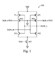
- transistor PPG1 is turned on, and voltage Vdd + Vrob is passed through transistor PPG1 to the bulk of transistor PO2.
- the bulk of transistor PO2 is provided with a re-offset voltage value of Vrob.
- Node NO21 pulled low also causes transistor P22 to turn on, which transfers voltage Vdd at the source of transistor P22 to the drain of transistor P22 or to the bulk of transistor PO1.
- Fig. 3 is a diagram of a circuit 300 illustrating re-offsetting to the bulk of both transistors PO1 and PO2.
- the bulk of transistor PO1 is re-offset with a first value, e.g., voltage Vrob1, by a sub-circuit 300A
- the bulk of transistor PO2 is re-offset with a second value, e.g., voltage Vrob2, by a sub-circuit 300B.
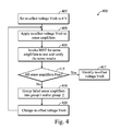
- step 405 re-offset voltage Vrob is set to 0 V.
- a sequential search e.g., voltage Vrobn keeps decreasing
- other searches including a binary search are within the scope of various embodiments.
- the re-offset operation of transistors NO1 and NO2 is substantially the same as that of transistors PO1 and PO2.
- voltage Vthn1 is greater than voltage Vthn2 (e.g., voltage ⁇ Vth is positive)
- a corresponding positive re-offset voltage Vrob is applied at the bulk of transistor NO2
- voltage Vthn2 is less than voltage Vthn2 (e.g., voltage ⁇ Vth is negative)
- a corresponding positive re-offset voltage Vrob is applied at the bulk of transistor NO1, etc.
- Different techniques e.g., having one or two re-offset voltages, negative and/or positive re-offset voltages, etc.
- SA 100 are applicable to SA 500 as would be recognizable by a person of ordinary skill in the art.
- a gate of the second transistor and a gate of the fourth transistor are coupled together and form a first data input for the amplifier.
- a gate of the third transistor and a gate of the first transistor are coupled together and form a second data input for the amplifier.
- Applying the compensation voltage value causes a reduction in a voltage difference between a first threshold voltage of the first transistor and a second threshold voltage of the second transistor.
- Some embodiments regard a method of re-offsetting a plurality of amplifier.
- the method includes testing the plurality of amplifiers based on a re-offset value at bulks of compensation transistors of the plurality of amplifiers; identifying a first group of first amplifiers of the plurality of amplifiers favoring reading a first logic level and/or a second group of second amplifiers of the plurality of amplifiers favoring reading a second logic level different from the first logic level, based on results of the testing step; changing the re-offset value to a new re-offset value; re-offsetting the first group of first amplifiers and/or the second group of second amplifiers based on the new re-offset value; and re-testing the first group of first amplifiers and the second group of second amplifiers.
Landscapes
- Engineering & Computer Science (AREA)
- Power Engineering (AREA)
- Physics & Mathematics (AREA)
- General Physics & Mathematics (AREA)
- Amplifiers (AREA)
Applications Claiming Priority (2)
| Application Number | Priority Date | Filing Date | Title |
|---|---|---|---|
| US12/903,652 US8362807B2 (en) | 2010-10-13 | 2010-10-13 | Offset compensation for sense amplifiers |
| EP11002116.9A EP2442311B1 (fr) | 2010-10-13 | 2011-03-14 | Compensation de décalage pour amplificateurs détecteurs |
Related Parent Applications (3)
| Application Number | Title | Priority Date | Filing Date |
|---|---|---|---|
| EP11002116.9 Division | 2011-03-14 | ||
| EP11002116.9A Division EP2442311B1 (fr) | 2010-10-13 | 2011-03-14 | Compensation de décalage pour amplificateurs détecteurs |
| EP11002116.9A Division-Into EP2442311B1 (fr) | 2010-10-13 | 2011-03-14 | Compensation de décalage pour amplificateurs détecteurs |
Publications (2)
| Publication Number | Publication Date |
|---|---|
| EP2631911A1 true EP2631911A1 (fr) | 2013-08-28 |
| EP2631911B1 EP2631911B1 (fr) | 2017-02-01 |
Family
ID=43971345
Family Applications (2)
| Application Number | Title | Priority Date | Filing Date |
|---|---|---|---|
| EP13169111.5A Active EP2631911B1 (fr) | 2010-10-13 | 2011-03-14 | Compensation de décalage pour amplificateurs détecteurs |
| EP11002116.9A Active EP2442311B1 (fr) | 2010-10-13 | 2011-03-14 | Compensation de décalage pour amplificateurs détecteurs |
Family Applications After (1)
| Application Number | Title | Priority Date | Filing Date |
|---|---|---|---|
| EP11002116.9A Active EP2442311B1 (fr) | 2010-10-13 | 2011-03-14 | Compensation de décalage pour amplificateurs détecteurs |
Country Status (4)
| Country | Link |
|---|---|
| US (3) | US8362807B2 (fr) |
| EP (2) | EP2631911B1 (fr) |
| CN (1) | CN102446537B (fr) |
| TW (1) | TWI469153B (fr) |
Cited By (1)
| Publication number | Priority date | Publication date | Assignee | Title |
|---|---|---|---|---|
| US12469533B2 (en) | 2023-09-27 | 2025-11-11 | Macronix International Co., Ltd. | Calibration apparatus and calibration method of memory device with strong-arm comparator |
Families Citing this family (22)
| Publication number | Priority date | Publication date | Assignee | Title |
|---|---|---|---|---|
| US8542551B2 (en) | 2011-07-29 | 2013-09-24 | Taiwan Semiconductor Manufacturing Company, Ltd. | Circuit and method for reducing leakage current |
| US8912825B2 (en) * | 2013-02-18 | 2014-12-16 | Macronix International Co., Ltd. | Sense amplifier system and sensing method thereof |
| WO2015033491A1 (fr) * | 2013-09-09 | 2015-03-12 | パナソニック株式会社 | Mémoire à semi-conducteurs et circuit amplificateur de lecture |
| US9384791B1 (en) | 2014-12-30 | 2016-07-05 | Altera Corporation | Apparatus and method for sense amplifier offset cancellation |
| CN105070310B (zh) * | 2015-08-11 | 2018-03-09 | 深圳芯邦科技股份有限公司 | 一种带失调校正的灵敏放大器 |
| US10199334B2 (en) | 2015-10-20 | 2019-02-05 | Infineon Technologies Ag | Digital circuit and method for manufacturing a digital circuit |
| US9799395B2 (en) * | 2015-11-30 | 2017-10-24 | Texas Instruments Incorporated | Sense amplifier in low power and high performance SRAM |
| US9825636B1 (en) * | 2016-10-20 | 2017-11-21 | Arm Limited | Apparatus and method for reduced latency signal synchronization |
| US10921839B2 (en) | 2017-08-30 | 2021-02-16 | Taiwan Semiconductor Manufacturing Co., Ltd. | Switchable power supply |
| DE102019123555B4 (de) | 2019-09-03 | 2022-12-01 | Infineon Technologies Ag | Physisch obfuskierter schaltkreis |
| CN114730586B (zh) * | 2020-02-06 | 2025-07-25 | 长鑫存储技术有限公司 | 感测放大器电路、存储器及其操作方法 |
| US10943644B1 (en) * | 2020-02-19 | 2021-03-09 | Micron Technology, Inc. | Apparatuses including threshold voltage compensated sense amplifiers and methods for compensating same |
| CN111913027A (zh) * | 2020-08-05 | 2020-11-10 | 青岛鼎信通讯股份有限公司 | 一种应用于电力电子变压器的高压宽频的电压检测电路 |
| CN111863054B (zh) * | 2020-08-13 | 2022-11-01 | 安徽大学 | 灵敏放大器、存储器和灵敏放大器的控制方法 |
| US11887655B2 (en) | 2020-08-13 | 2024-01-30 | Anhui University | Sense amplifier, memory, and method for controlling sense amplifier by configuring structures using switches |
| US11862285B2 (en) | 2020-09-01 | 2024-01-02 | Anhui University | Sense amplifier, memory and control method of sense amplifier |
| US11929111B2 (en) | 2020-09-01 | 2024-03-12 | Anhui University | Sense amplifier, memory and method for controlling sense amplifier |
| CN111933195B (zh) * | 2020-09-01 | 2022-11-01 | 安徽大学 | 灵敏放大器、存储器和灵敏放大器的控制方法 |
| TWI762317B (zh) * | 2021-05-17 | 2022-04-21 | 力晶積成電子製造股份有限公司 | 感測電路以及測試裝置 |
| KR20240041626A (ko) | 2022-09-23 | 2024-04-01 | 삼성전자주식회사 | 감지 증폭기, 이의 동작 방법 및 이를 포함하는 휘발성 메모리 장치 |
| CN118072786A (zh) * | 2022-11-23 | 2024-05-24 | 兆易创新科技集团股份有限公司 | 一种随机存储器及其灵敏放大补偿电路 |
| TWI875215B (zh) * | 2023-09-27 | 2025-03-01 | 旺宏電子股份有限公司 | 記憶體裝置的校準設備及其校準方法 |
Citations (4)
| Publication number | Priority date | Publication date | Assignee | Title |
|---|---|---|---|---|
| EP1104092A2 (fr) * | 1999-10-29 | 2001-05-30 | Hewlett-Packard Company, A Delaware Corporation | Amplificateur opérationnel à calibrage numérique d'offset |
| US20020024851A1 (en) * | 2000-06-28 | 2002-02-28 | Atsushi Kawasumi | Semiconductor integrated circuit |
| US20040136253A1 (en) * | 2002-10-07 | 2004-07-15 | Stmicroelectronics Pvt. Ltd. | Latch-type sense amplifier |
| US20100067318A1 (en) * | 2008-09-18 | 2010-03-18 | Nec Electronics Corporation | Sense amplifier and semiconductor memory device having sense amplifier |
Family Cites Families (15)
| Publication number | Priority date | Publication date | Assignee | Title |
|---|---|---|---|---|
| US5053996A (en) * | 1991-02-26 | 1991-10-01 | Sgs-Thomson Microelectronics, Inc. | Dual state memory storage cell with improved data transfer circuitry |
| US5424985A (en) * | 1993-06-30 | 1995-06-13 | Sgs-Thomson Microelectronics, Inc. | Compensating delay element for clock generation in a memory device |
| US6181621B1 (en) * | 1999-12-10 | 2001-01-30 | Cypress Semiconductor Corp. | Threshold voltage mismatch compensated sense amplifier for SRAM memory arrays |
| US7164612B1 (en) * | 2003-10-10 | 2007-01-16 | Sun Microsystems, Inc. | Test circuit for measuring sense amplifier and memory mismatches |
| US7020035B1 (en) * | 2003-10-10 | 2006-03-28 | Sun Microsystems, Inc. | Measuring and correcting sense amplifier and memory mismatches using NBTI |
| US7466613B2 (en) * | 2005-04-15 | 2008-12-16 | Atmel Corporation | Sense amplifier for flash memory device |
| US7372746B2 (en) * | 2005-08-17 | 2008-05-13 | Micron Technology, Inc. | Low voltage sensing scheme having reduced active power down standby current |
| US7405988B2 (en) * | 2005-09-26 | 2008-07-29 | Silicon Storage Technology, Inc. | Method and apparatus for systematic and random variation and mismatch compensation for multilevel flash memory operation |
| JP4744325B2 (ja) * | 2006-03-02 | 2011-08-10 | ルネサスエレクトロニクス株式会社 | 信号増幅器 |
| KR100752669B1 (ko) * | 2006-08-22 | 2007-08-29 | 삼성전자주식회사 | 오픈 비트 라인 구조를 가지는 반도체 메모리 장치의 비트라인 센스 앰프 |
| US7738306B2 (en) * | 2007-12-07 | 2010-06-15 | Etron Technology, Inc. | Method to improve the write speed for memory products |
| JP5197241B2 (ja) * | 2008-09-01 | 2013-05-15 | ルネサスエレクトロニクス株式会社 | 半導体装置 |
| JP5321800B2 (ja) * | 2008-10-10 | 2013-10-23 | 株式会社東芝 | センスアンプ制御回路 |
| CN101807422B (zh) * | 2010-03-26 | 2013-03-20 | 上海宏力半导体制造有限公司 | 读出放大电路 |
| EP2871486A4 (fr) * | 2012-07-06 | 2016-03-16 | Alps Green Devices Co Ltd | Procédé de fabrication d'un capteur de courant, et capteur de courant |
-
2010
- 2010-10-13 US US12/903,652 patent/US8362807B2/en not_active Expired - Fee Related
-
2011
- 2011-03-14 EP EP13169111.5A patent/EP2631911B1/fr active Active
- 2011-03-14 EP EP11002116.9A patent/EP2442311B1/fr active Active
- 2011-03-30 TW TW100110967A patent/TWI469153B/zh not_active IP Right Cessation
- 2011-09-28 CN CN201110299278.XA patent/CN102446537B/zh not_active Expired - Fee Related
-
2012
- 2012-12-27 US US13/728,637 patent/US9322859B2/en not_active Expired - Fee Related
-
2016
- 2016-01-07 US US14/990,000 patent/US9509255B2/en not_active Expired - Fee Related
Patent Citations (4)
| Publication number | Priority date | Publication date | Assignee | Title |
|---|---|---|---|---|
| EP1104092A2 (fr) * | 1999-10-29 | 2001-05-30 | Hewlett-Packard Company, A Delaware Corporation | Amplificateur opérationnel à calibrage numérique d'offset |
| US20020024851A1 (en) * | 2000-06-28 | 2002-02-28 | Atsushi Kawasumi | Semiconductor integrated circuit |
| US20040136253A1 (en) * | 2002-10-07 | 2004-07-15 | Stmicroelectronics Pvt. Ltd. | Latch-type sense amplifier |
| US20100067318A1 (en) * | 2008-09-18 | 2010-03-18 | Nec Electronics Corporation | Sense amplifier and semiconductor memory device having sense amplifier |
Cited By (1)
| Publication number | Priority date | Publication date | Assignee | Title |
|---|---|---|---|---|
| US12469533B2 (en) | 2023-09-27 | 2025-11-11 | Macronix International Co., Ltd. | Calibration apparatus and calibration method of memory device with strong-arm comparator |
Also Published As
| Publication number | Publication date |
|---|---|
| US8362807B2 (en) | 2013-01-29 |
| US20130113552A1 (en) | 2013-05-09 |
| TWI469153B (zh) | 2015-01-11 |
| US20160118945A1 (en) | 2016-04-28 |
| CN102446537B (zh) | 2014-03-12 |
| US9509255B2 (en) | 2016-11-29 |
| US9322859B2 (en) | 2016-04-26 |
| EP2631911B1 (fr) | 2017-02-01 |
| CN102446537A (zh) | 2012-05-09 |
| US20120092072A1 (en) | 2012-04-19 |
| TW201216291A (en) | 2012-04-16 |
| EP2442311B1 (fr) | 2015-08-12 |
| EP2442311A1 (fr) | 2012-04-18 |
Similar Documents
| Publication | Publication Date | Title |
|---|---|---|
| EP2631911A1 (fr) | Compensation de décalage pour amplificateurs détecteurs | |
| US7724565B2 (en) | Apparatus and method for small signal sensing in an SRAM cell utilizing PFET access devices | |
| KR100871673B1 (ko) | 반도체 메모리 장치의 센스 앰프 회로 및 그 동작 방법 | |
| US9257995B2 (en) | Apparatuses and methods for mitigating uneven circuit degradation of delay circuits | |
| EP3622514A1 (fr) | Amplification de signal d'amplificateur de détection | |
| US8208313B2 (en) | Static random access memory (SRAM) and test method of the SRAM having precharge circuit to precharge bit line | |
| US20020024851A1 (en) | Semiconductor integrated circuit | |
| US7164612B1 (en) | Test circuit for measuring sense amplifier and memory mismatches | |
| US6778450B2 (en) | Programmable weak write test mode | |
| US20190108895A1 (en) | Margin test for one-time programmable memory (otpm) array with common mode current source | |
| US9374072B2 (en) | Post fabrication tuning of an integrated circuit | |
| US20030198088A1 (en) | Voltage detection circuit and method for semiconductor memory devices | |
| US20210183436A1 (en) | Voltage Retention Techniques | |
| US7020035B1 (en) | Measuring and correcting sense amplifier and memory mismatches using NBTI | |
| US7590010B2 (en) | Data output circuit in semiconductor memory device | |
| JP2010182344A (ja) | SRAM(StaticRandomAccessMemory)、及びSRAMのテスト方法 | |
| US12125552B2 (en) | Determination circuit and correction method | |
| US20090190426A1 (en) | Circuits, methods and design structures for adaptive repair of sram arrays | |
| KR101014996B1 (ko) | 테스트 효율을 개선시키는 오픈 비트 라인 타입 반도체메모리 장치의 비트 라인 센스 앰프 회로 | |
| Vatajelu et al. | Transient noise failures in SRAM cells: Dynamic noise margin metric | |
| KR100837803B1 (ko) | 전압 검출 장치 및 이를 포함하는 내부 전압 발생 장치 | |
| US20170062043A1 (en) | Dynamic Capacitance Balancing | |
| KR100668501B1 (ko) | 반도체 메모리의 센스 앰프 테스트 장치 및 방법 | |
| JP2011159331A (ja) | 半導体記憶装置 | |
| Prasad | A New Memory Architecture |
Legal Events
| Date | Code | Title | Description |
|---|---|---|---|
| PUAI | Public reference made under article 153(3) epc to a published international application that has entered the european phase |
Free format text: ORIGINAL CODE: 0009012 |
|
| AC | Divisional application: reference to earlier application |
Ref document number: 2442311 Country of ref document: EP Kind code of ref document: P |
|
| AK | Designated contracting states |
Kind code of ref document: A1 Designated state(s): AL AT BE BG CH CY CZ DE DK EE ES FI FR GB GR HR HU IE IS IT LI LT LU LV MC MK MT NL NO PL PT RO RS SE SI SK SM TR |
|
| 17P | Request for examination filed |
Effective date: 20140225 |
|
| RBV | Designated contracting states (corrected) |
Designated state(s): AL AT BE BG CH CY CZ DE DK EE ES FI FR GB GR HR HU IE IS IT LI LT LU LV MC MK MT NL NO PL PT RO RS SE SI SK SM TR |
|
| 17Q | First examination report despatched |
Effective date: 20140806 |
|
| GRAJ | Information related to disapproval of communication of intention to grant by the applicant or resumption of examination proceedings by the epo deleted |
Free format text: ORIGINAL CODE: EPIDOSDIGR1 |
|
| GRAP | Despatch of communication of intention to grant a patent |
Free format text: ORIGINAL CODE: EPIDOSNIGR1 |
|
| INTG | Intention to grant announced |
Effective date: 20160822 |
|
| RIN1 | Information on inventor provided before grant (corrected) |
Inventor name: SAMPIGETHAYA, SHREEKANTH Inventor name: UPPUTURI, BHARATH |
|
| GRAS | Grant fee paid |
Free format text: ORIGINAL CODE: EPIDOSNIGR3 |
|
| GRAA | (expected) grant |
Free format text: ORIGINAL CODE: 0009210 |
|
| AC | Divisional application: reference to earlier application |
Ref document number: 2442311 Country of ref document: EP Kind code of ref document: P |
|
| AK | Designated contracting states |
Kind code of ref document: B1 Designated state(s): AL AT BE BG CH CY CZ DE DK EE ES FI FR GB GR HR HU IE IS IT LI LT LU LV MC MK MT NL NO PL PT RO RS SE SI SK SM TR |
|
| REG | Reference to a national code |
Ref country code: GB Ref legal event code: FG4D |
|
| REG | Reference to a national code |
Ref country code: CH Ref legal event code: EP Ref country code: AT Ref legal event code: REF Ref document number: 866141 Country of ref document: AT Kind code of ref document: T Effective date: 20170215 |
|
| REG | Reference to a national code |
Ref country code: IE Ref legal event code: FG4D |
|
| REG | Reference to a national code |
Ref country code: DE Ref legal event code: R096 Ref document number: 602011034877 Country of ref document: DE |
|
| REG | Reference to a national code |
Ref country code: NL Ref legal event code: MP Effective date: 20170201 |
|
| REG | Reference to a national code |
Ref country code: LT Ref legal event code: MG4D |
|
| REG | Reference to a national code |
Ref country code: AT Ref legal event code: MK05 Ref document number: 866141 Country of ref document: AT Kind code of ref document: T Effective date: 20170201 |
|
| PG25 | Lapsed in a contracting state [announced via postgrant information from national office to epo] |
Ref country code: LT Free format text: LAPSE BECAUSE OF FAILURE TO SUBMIT A TRANSLATION OF THE DESCRIPTION OR TO PAY THE FEE WITHIN THE PRESCRIBED TIME-LIMIT Effective date: 20170201 Ref country code: GR Free format text: LAPSE BECAUSE OF FAILURE TO SUBMIT A TRANSLATION OF THE DESCRIPTION OR TO PAY THE FEE WITHIN THE PRESCRIBED TIME-LIMIT Effective date: 20170502 Ref country code: NO Free format text: LAPSE BECAUSE OF FAILURE TO SUBMIT A TRANSLATION OF THE DESCRIPTION OR TO PAY THE FEE WITHIN THE PRESCRIBED TIME-LIMIT Effective date: 20170501 Ref country code: HR Free format text: LAPSE BECAUSE OF FAILURE TO SUBMIT A TRANSLATION OF THE DESCRIPTION OR TO PAY THE FEE WITHIN THE PRESCRIBED TIME-LIMIT Effective date: 20170201 Ref country code: FI Free format text: LAPSE BECAUSE OF FAILURE TO SUBMIT A TRANSLATION OF THE DESCRIPTION OR TO PAY THE FEE WITHIN THE PRESCRIBED TIME-LIMIT Effective date: 20170201 Ref country code: IS Free format text: LAPSE BECAUSE OF FAILURE TO SUBMIT A TRANSLATION OF THE DESCRIPTION OR TO PAY THE FEE WITHIN THE PRESCRIBED TIME-LIMIT Effective date: 20170601 |
|
| PG25 | Lapsed in a contracting state [announced via postgrant information from national office to epo] |
Ref country code: LV Free format text: LAPSE BECAUSE OF FAILURE TO SUBMIT A TRANSLATION OF THE DESCRIPTION OR TO PAY THE FEE WITHIN THE PRESCRIBED TIME-LIMIT Effective date: 20170201 Ref country code: PL Free format text: LAPSE BECAUSE OF FAILURE TO SUBMIT A TRANSLATION OF THE DESCRIPTION OR TO PAY THE FEE WITHIN THE PRESCRIBED TIME-LIMIT Effective date: 20170201 Ref country code: SE Free format text: LAPSE BECAUSE OF FAILURE TO SUBMIT A TRANSLATION OF THE DESCRIPTION OR TO PAY THE FEE WITHIN THE PRESCRIBED TIME-LIMIT Effective date: 20170201 Ref country code: PT Free format text: LAPSE BECAUSE OF FAILURE TO SUBMIT A TRANSLATION OF THE DESCRIPTION OR TO PAY THE FEE WITHIN THE PRESCRIBED TIME-LIMIT Effective date: 20170601 Ref country code: BG Free format text: LAPSE BECAUSE OF FAILURE TO SUBMIT A TRANSLATION OF THE DESCRIPTION OR TO PAY THE FEE WITHIN THE PRESCRIBED TIME-LIMIT Effective date: 20170501 Ref country code: ES Free format text: LAPSE BECAUSE OF FAILURE TO SUBMIT A TRANSLATION OF THE DESCRIPTION OR TO PAY THE FEE WITHIN THE PRESCRIBED TIME-LIMIT Effective date: 20170201 Ref country code: AT Free format text: LAPSE BECAUSE OF FAILURE TO SUBMIT A TRANSLATION OF THE DESCRIPTION OR TO PAY THE FEE WITHIN THE PRESCRIBED TIME-LIMIT Effective date: 20170201 Ref country code: NL Free format text: LAPSE BECAUSE OF FAILURE TO SUBMIT A TRANSLATION OF THE DESCRIPTION OR TO PAY THE FEE WITHIN THE PRESCRIBED TIME-LIMIT Effective date: 20170201 Ref country code: RS Free format text: LAPSE BECAUSE OF FAILURE TO SUBMIT A TRANSLATION OF THE DESCRIPTION OR TO PAY THE FEE WITHIN THE PRESCRIBED TIME-LIMIT Effective date: 20170201 |
|
| PG25 | Lapsed in a contracting state [announced via postgrant information from national office to epo] |
Ref country code: CZ Free format text: LAPSE BECAUSE OF FAILURE TO SUBMIT A TRANSLATION OF THE DESCRIPTION OR TO PAY THE FEE WITHIN THE PRESCRIBED TIME-LIMIT Effective date: 20170201 Ref country code: SK Free format text: LAPSE BECAUSE OF FAILURE TO SUBMIT A TRANSLATION OF THE DESCRIPTION OR TO PAY THE FEE WITHIN THE PRESCRIBED TIME-LIMIT Effective date: 20170201 Ref country code: EE Free format text: LAPSE BECAUSE OF FAILURE TO SUBMIT A TRANSLATION OF THE DESCRIPTION OR TO PAY THE FEE WITHIN THE PRESCRIBED TIME-LIMIT Effective date: 20170201 Ref country code: RO Free format text: LAPSE BECAUSE OF FAILURE TO SUBMIT A TRANSLATION OF THE DESCRIPTION OR TO PAY THE FEE WITHIN THE PRESCRIBED TIME-LIMIT Effective date: 20170201 Ref country code: IT Free format text: LAPSE BECAUSE OF FAILURE TO SUBMIT A TRANSLATION OF THE DESCRIPTION OR TO PAY THE FEE WITHIN THE PRESCRIBED TIME-LIMIT Effective date: 20170201 |
|
| REG | Reference to a national code |
Ref country code: CH Ref legal event code: PL |
|
| REG | Reference to a national code |
Ref country code: DE Ref legal event code: R097 Ref document number: 602011034877 Country of ref document: DE |
|
| PG25 | Lapsed in a contracting state [announced via postgrant information from national office to epo] |
Ref country code: DK Free format text: LAPSE BECAUSE OF FAILURE TO SUBMIT A TRANSLATION OF THE DESCRIPTION OR TO PAY THE FEE WITHIN THE PRESCRIBED TIME-LIMIT Effective date: 20170201 Ref country code: SM Free format text: LAPSE BECAUSE OF FAILURE TO SUBMIT A TRANSLATION OF THE DESCRIPTION OR TO PAY THE FEE WITHIN THE PRESCRIBED TIME-LIMIT Effective date: 20170201 Ref country code: MC Free format text: LAPSE BECAUSE OF FAILURE TO SUBMIT A TRANSLATION OF THE DESCRIPTION OR TO PAY THE FEE WITHIN THE PRESCRIBED TIME-LIMIT Effective date: 20170201 |
|
| PLBE | No opposition filed within time limit |
Free format text: ORIGINAL CODE: 0009261 |
|
| STAA | Information on the status of an ep patent application or granted ep patent |
Free format text: STATUS: NO OPPOSITION FILED WITHIN TIME LIMIT |
|
| REG | Reference to a national code |
Ref country code: IE Ref legal event code: MM4A |
|
| REG | Reference to a national code |
Ref country code: FR Ref legal event code: ST Effective date: 20171130 |
|
| 26N | No opposition filed |
Effective date: 20171103 |
|
| GBPC | Gb: european patent ceased through non-payment of renewal fee |
Effective date: 20170501 |
|
| PG25 | Lapsed in a contracting state [announced via postgrant information from national office to epo] |
Ref country code: FR Free format text: LAPSE BECAUSE OF NON-PAYMENT OF DUE FEES Effective date: 20170403 Ref country code: LU Free format text: LAPSE BECAUSE OF NON-PAYMENT OF DUE FEES Effective date: 20170314 |
|
| PG25 | Lapsed in a contracting state [announced via postgrant information from national office to epo] |
Ref country code: LI Free format text: LAPSE BECAUSE OF NON-PAYMENT OF DUE FEES Effective date: 20170331 Ref country code: CH Free format text: LAPSE BECAUSE OF NON-PAYMENT OF DUE FEES Effective date: 20170331 Ref country code: IE Free format text: LAPSE BECAUSE OF NON-PAYMENT OF DUE FEES Effective date: 20170314 Ref country code: SI Free format text: LAPSE BECAUSE OF FAILURE TO SUBMIT A TRANSLATION OF THE DESCRIPTION OR TO PAY THE FEE WITHIN THE PRESCRIBED TIME-LIMIT Effective date: 20170201 |
|
| REG | Reference to a national code |
Ref country code: BE Ref legal event code: MM Effective date: 20170331 |
|
| PG25 | Lapsed in a contracting state [announced via postgrant information from national office to epo] |
Ref country code: GB Free format text: LAPSE BECAUSE OF NON-PAYMENT OF DUE FEES Effective date: 20170501 |
|
| PG25 | Lapsed in a contracting state [announced via postgrant information from national office to epo] |
Ref country code: BE Free format text: LAPSE BECAUSE OF NON-PAYMENT OF DUE FEES Effective date: 20170331 |
|
| PG25 | Lapsed in a contracting state [announced via postgrant information from national office to epo] |
Ref country code: MT Free format text: LAPSE BECAUSE OF NON-PAYMENT OF DUE FEES Effective date: 20170314 |
|
| PG25 | Lapsed in a contracting state [announced via postgrant information from national office to epo] |
Ref country code: HU Free format text: LAPSE BECAUSE OF FAILURE TO SUBMIT A TRANSLATION OF THE DESCRIPTION OR TO PAY THE FEE WITHIN THE PRESCRIBED TIME-LIMIT; INVALID AB INITIO Effective date: 20110314 |
|
| PG25 | Lapsed in a contracting state [announced via postgrant information from national office to epo] |
Ref country code: CY Free format text: LAPSE BECAUSE OF NON-PAYMENT OF DUE FEES Effective date: 20170201 |
|
| PG25 | Lapsed in a contracting state [announced via postgrant information from national office to epo] |
Ref country code: MK Free format text: LAPSE BECAUSE OF FAILURE TO SUBMIT A TRANSLATION OF THE DESCRIPTION OR TO PAY THE FEE WITHIN THE PRESCRIBED TIME-LIMIT Effective date: 20170201 |
|
| PG25 | Lapsed in a contracting state [announced via postgrant information from national office to epo] |
Ref country code: TR Free format text: LAPSE BECAUSE OF FAILURE TO SUBMIT A TRANSLATION OF THE DESCRIPTION OR TO PAY THE FEE WITHIN THE PRESCRIBED TIME-LIMIT Effective date: 20170201 |
|
| PG25 | Lapsed in a contracting state [announced via postgrant information from national office to epo] |
Ref country code: AL Free format text: LAPSE BECAUSE OF FAILURE TO SUBMIT A TRANSLATION OF THE DESCRIPTION OR TO PAY THE FEE WITHIN THE PRESCRIBED TIME-LIMIT Effective date: 20170201 |
|
| PGFP | Annual fee paid to national office [announced via postgrant information from national office to epo] |
Ref country code: DE Payment date: 20260327 Year of fee payment: 16 |