EP2631941A2 - Verfahren zur Bildung einer Chipanordnung mit Wärmeverteiler - Google Patents
Verfahren zur Bildung einer Chipanordnung mit Wärmeverteiler Download PDFInfo
- Publication number
- EP2631941A2 EP2631941A2 EP13151824.3A EP13151824A EP2631941A2 EP 2631941 A2 EP2631941 A2 EP 2631941A2 EP 13151824 A EP13151824 A EP 13151824A EP 2631941 A2 EP2631941 A2 EP 2631941A2
- Authority
- EP
- European Patent Office
- Prior art keywords
- die
- heat spreader
- major surface
- thermoset material
- package substrate
- Prior art date
- Legal status (The legal status is an assumption and is not a legal conclusion. Google has not performed a legal analysis and makes no representation as to the accuracy of the status listed.)
- Withdrawn
Links
Images

Classifications
-
- H—ELECTRICITY
- H10—SEMICONDUCTOR DEVICES; ELECTRIC SOLID-STATE DEVICES NOT OTHERWISE PROVIDED FOR
- H10W—GENERIC PACKAGES, INTERCONNECTIONS, CONNECTORS OR OTHER CONSTRUCTIONAL DETAILS OF DEVICES COVERED BY CLASS H10
- H10W40/00—Arrangements for thermal protection or thermal control
- H10W40/70—Fillings or auxiliary members in containers or in encapsulations for thermal protection or control
- H10W40/77—Auxiliary members characterised by their shape
- H10W40/778—Auxiliary members characterised by their shape in encapsulations
-
- H—ELECTRICITY
- H10—SEMICONDUCTOR DEVICES; ELECTRIC SOLID-STATE DEVICES NOT OTHERWISE PROVIDED FOR
- H10W—GENERIC PACKAGES, INTERCONNECTIONS, CONNECTORS OR OTHER CONSTRUCTIONAL DETAILS OF DEVICES COVERED BY CLASS H10
- H10W74/00—Encapsulations, e.g. protective coatings
- H10W74/01—Manufacture or treatment
- H10W74/016—Manufacture or treatment using moulds
- H10W74/017—Auxiliary layers for moulds, e.g. release layers or layers preventing residue
-
- H—ELECTRICITY
- H10—SEMICONDUCTOR DEVICES; ELECTRIC SOLID-STATE DEVICES NOT OTHERWISE PROVIDED FOR
- H10W—GENERIC PACKAGES, INTERCONNECTIONS, CONNECTORS OR OTHER CONSTRUCTIONAL DETAILS OF DEVICES COVERED BY CLASS H10
- H10W72/00—Interconnections or connectors in packages
- H10W72/851—Dispositions of multiple connectors or interconnections
- H10W72/853—On the same surface
- H10W72/865—Die-attach connectors and bond wires
-
- H—ELECTRICITY
- H10—SEMICONDUCTOR DEVICES; ELECTRIC SOLID-STATE DEVICES NOT OTHERWISE PROVIDED FOR
- H10W—GENERIC PACKAGES, INTERCONNECTIONS, CONNECTORS OR OTHER CONSTRUCTIONAL DETAILS OF DEVICES COVERED BY CLASS H10
- H10W72/00—Interconnections or connectors in packages
- H10W72/851—Dispositions of multiple connectors or interconnections
- H10W72/874—On different surfaces
- H10W72/877—Bump connectors and die-attach connectors
-
- H—ELECTRICITY
- H10—SEMICONDUCTOR DEVICES; ELECTRIC SOLID-STATE DEVICES NOT OTHERWISE PROVIDED FOR
- H10W—GENERIC PACKAGES, INTERCONNECTIONS, CONNECTORS OR OTHER CONSTRUCTIONAL DETAILS OF DEVICES COVERED BY CLASS H10
- H10W72/00—Interconnections or connectors in packages
- H10W72/851—Dispositions of multiple connectors or interconnections
- H10W72/874—On different surfaces
- H10W72/884—Die-attach connectors and bond wires
-
- H—ELECTRICITY
- H10—SEMICONDUCTOR DEVICES; ELECTRIC SOLID-STATE DEVICES NOT OTHERWISE PROVIDED FOR
- H10W—GENERIC PACKAGES, INTERCONNECTIONS, CONNECTORS OR OTHER CONSTRUCTIONAL DETAILS OF DEVICES COVERED BY CLASS H10
- H10W74/00—Encapsulations, e.g. protective coatings
- H10W74/10—Encapsulations, e.g. protective coatings characterised by their shape or disposition
-
- H—ELECTRICITY
- H10—SEMICONDUCTOR DEVICES; ELECTRIC SOLID-STATE DEVICES NOT OTHERWISE PROVIDED FOR
- H10W—GENERIC PACKAGES, INTERCONNECTIONS, CONNECTORS OR OTHER CONSTRUCTIONAL DETAILS OF DEVICES COVERED BY CLASS H10
- H10W74/00—Encapsulations, e.g. protective coatings
- H10W74/10—Encapsulations, e.g. protective coatings characterised by their shape or disposition
- H10W74/111—Encapsulations, e.g. protective coatings characterised by their shape or disposition the semiconductor body being completely enclosed
- H10W74/114—Encapsulations, e.g. protective coatings characterised by their shape or disposition the semiconductor body being completely enclosed by a substrate and the encapsulations
- H10W74/117—Encapsulations, e.g. protective coatings characterised by their shape or disposition the semiconductor body being completely enclosed by a substrate and the encapsulations the substrate having spherical bumps for external connection
-
- H—ELECTRICITY
- H10—SEMICONDUCTOR DEVICES; ELECTRIC SOLID-STATE DEVICES NOT OTHERWISE PROVIDED FOR
- H10W—GENERIC PACKAGES, INTERCONNECTIONS, CONNECTORS OR OTHER CONSTRUCTIONAL DETAILS OF DEVICES COVERED BY CLASS H10
- H10W90/00—Package configurations
- H10W90/701—Package configurations characterised by the relative positions of pads or connectors relative to package parts
- H10W90/721—Package configurations characterised by the relative positions of pads or connectors relative to package parts of bump connectors
- H10W90/724—Package configurations characterised by the relative positions of pads or connectors relative to package parts of bump connectors between a chip and a stacked insulating package substrate, interposer or RDL
-
- H—ELECTRICITY
- H10—SEMICONDUCTOR DEVICES; ELECTRIC SOLID-STATE DEVICES NOT OTHERWISE PROVIDED FOR
- H10W—GENERIC PACKAGES, INTERCONNECTIONS, CONNECTORS OR OTHER CONSTRUCTIONAL DETAILS OF DEVICES COVERED BY CLASS H10
- H10W90/00—Package configurations
- H10W90/701—Package configurations characterised by the relative positions of pads or connectors relative to package parts
- H10W90/731—Package configurations characterised by the relative positions of pads or connectors relative to package parts of die-attach connectors
- H10W90/734—Package configurations characterised by the relative positions of pads or connectors relative to package parts of die-attach connectors between a chip and a stacked insulating package substrate, interposer or RDL
-
- H—ELECTRICITY
- H10—SEMICONDUCTOR DEVICES; ELECTRIC SOLID-STATE DEVICES NOT OTHERWISE PROVIDED FOR
- H10W—GENERIC PACKAGES, INTERCONNECTIONS, CONNECTORS OR OTHER CONSTRUCTIONAL DETAILS OF DEVICES COVERED BY CLASS H10
- H10W90/00—Package configurations
- H10W90/701—Package configurations characterised by the relative positions of pads or connectors relative to package parts
- H10W90/731—Package configurations characterised by the relative positions of pads or connectors relative to package parts of die-attach connectors
- H10W90/736—Package configurations characterised by the relative positions of pads or connectors relative to package parts of die-attach connectors between a chip and a stacked lead frame, conducting package substrate or heat sink
-
- H—ELECTRICITY
- H10—SEMICONDUCTOR DEVICES; ELECTRIC SOLID-STATE DEVICES NOT OTHERWISE PROVIDED FOR
- H10W—GENERIC PACKAGES, INTERCONNECTIONS, CONNECTORS OR OTHER CONSTRUCTIONAL DETAILS OF DEVICES COVERED BY CLASS H10
- H10W90/00—Package configurations
- H10W90/701—Package configurations characterised by the relative positions of pads or connectors relative to package parts
- H10W90/751—Package configurations characterised by the relative positions of pads or connectors relative to package parts of bond wires
- H10W90/754—Package configurations characterised by the relative positions of pads or connectors relative to package parts of bond wires between a chip and a stacked insulating package substrate, interposer or RDL
-
- H—ELECTRICITY
- H10—SEMICONDUCTOR DEVICES; ELECTRIC SOLID-STATE DEVICES NOT OTHERWISE PROVIDED FOR
- H10W—GENERIC PACKAGES, INTERCONNECTIONS, CONNECTORS OR OTHER CONSTRUCTIONAL DETAILS OF DEVICES COVERED BY CLASS H10
- H10W90/00—Package configurations
- H10W90/701—Package configurations characterised by the relative positions of pads or connectors relative to package parts
- H10W90/751—Package configurations characterised by the relative positions of pads or connectors relative to package parts of bond wires
- H10W90/756—Package configurations characterised by the relative positions of pads or connectors relative to package parts of bond wires between a chip and a stacked lead frame, conducting package substrate or heat sink
Definitions
- This disclosure relates generally to semiconductor devices, and more specifically, to a method of forming a semiconductor package with a heat spreader.
- Heat is generated by an integrated circuit (IC) die during operation. If inadequately removed, the heat generated by the die may cause the device to fail or to perform erratically. As such, heat spreaders are often incorporated into semiconductor packages to improve the thermal performance of the IC.
- IC integrated circuit
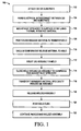
- FIG. 1 is a flow diagram of an embodiment of a method for forming a semiconductor die assembly with an integrated heat spreader.
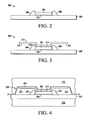
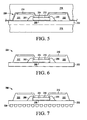
- FIGs. 2-7 show embodiments of a die assembly with an integrated heat spreader during successive stages of processing.
- FIG. 8 shows another embodiment of a die assembly with an integrated heat spreader.
- FIG. 9 shows another embodiment of a die assembly with an integrated heater spreader.
- FIG. 10 shows another embodiment of a die assembly with an integrated heater spreader.
- Embodiments of methods and assemblies disclosed herein greatly improve the thermal dissipation of transfer molded packages using a technique of bonding of a heat spreader directly to the junction surface of an integrated circuit die, or directly to the back side of a flip chip die and molding a package around the die/heat spreader assembly.
- Transfer molding may include a process called film assisted molding (FAM) which uses a soft film as a gasket material between a mold tool pedestal and the heat spreader.
- FAM film assisted molding
- Heat spreaders of various designs are attached to a surface of the IC die with a compliant thermal interface material (TIM) that bonds the heat spreader to the die.
- TIM compliant thermal interface material
- the heat spreader and die are assembled before the mold operation.
- the heat spreader can have many variations not known with other thermally enhanced BGAs (e.g.
- heat spreader may have protrusions that extend partially or all the way to the substrate surface, not just the die face region).
- the processes disclosed herein can be applied to many types packages such as PBGA, Fine Pitch BGA / MAPBGA, any form of QFP, QFN, PQFN, SOIC, TSSOP, etc. as well as multichip / System-in-Package configurations.
- FIG. 1 is a flow diagram of an embodiment of a method for forming a semiconductor die assembly with an integrated heat spreader.
- Process 102 can include attaching an IC die on a substrate.
- FIG. 2 shows an example of IC die 204 attached to substrate 202.
- the IC die 204 can be a flip chip or a wire bond die.
- the substrate 202 can be a lead frame or other type of semiconductor packaging substrate.
- the IC die 204 can be attached using a layer of die attach material 208 such as an adhesive paste or film. While FIG. 2 shows only a single die assembly 200 for purposes of simplicity, it is understood that the die assembly described herein may be applied to an array of die assemblies formed on a lead frame or other type of substrate array.
- electrical interconnects are formed between the IC die 204 and the substrate 202.
- the electrical interconnects can include wire bonds 206.
- the electrical interconnects can be established by bumps on a flip chip (not shown in FIG. 1 or 2 ) that contact electrical contacts on the substrate.
- Other suitable techniques for establishing electrical interconnectivity between the IC die 204 and the substrate 202 can be used.
- FIG. 3 shows an IC die/heat spreader assembly 209 formed by process 106.
- Process 106 can include mounting a heat spreader 212 to the surface of the IC die 204 so that at least a portion of the heat spreader 212 is bonded to a portion of the IC die 204.
- the heat spreader 212 is usually formed of a thermally conductive material such as a metal and can extend up to the edge of the substrate 202 or less to provide the desired amount of heat dissipation.
- the heat spreader 212 can include a pedestal portion 213 that contacts IC die 204.
- the pedestal portion 213 is formed or stamped, or etched, to raise the outer edges of the heat spreader 212 so that the heat spreader 212 does not contact or interfere with wire bonds 206 around the edges of IC die 204.
- the heat spreader 212 can be flat.
- Pedestal portion 213 can have any suitable shape.
- pedestal portion is formed by a flat sheet of material that is stamped in a central area so that the central area extends below side extensions 215.
- the material thickness of pedestal portion 213 is approximately the same as the side extensions 215.
- pedestal portion 213 can be solid, with the top of pedestal portion 213 flush with the top of side extensions 215 and pedestal portion 213 being thicker than side extensions 215.
- a thermal interface material 210 can be used to mount or attach or bond the heat spreader 212 to the IC die 204.
- the thermal interface material 210 can be a filled silicone gel material, a filled epoxy material, a filled grease, or other suitable material that is capable of withstanding subsequent assembly operations and operational conditions at expected temperatures and has good heat transfer characteristics.
- FIG. 4 shows an IC die/heat spreader assembly 209 between upper and lower portions of a film assisted molding (FAM)) transfer mold 216, 218.
- Process 108 can include positioning a layer of a die release material 214 between transfer mold 216 and the heat spreader 212, and in some embodiments between substrate 202 and transfer mold 218.
- the die release material 214 can be ethyltetrafluoroethylene (ETFE) or other suitable material.
- EFE ethyltetrafluoroethylene
- the die release material 214 can be positioned in upper and lower transfer molds 216, 218.
- the term "mold compound” refers to thermoset transfer mold compound.
- Process 110 can include applying a vacuum force to conform the die release material 214 to the shape of the upper and/or lower transfer molds 216, 218.
- process 112 can include inserting the IC die/heat spreader assembly 209 between upper transfer mold 216 and lower transfer mold 218. Once the IC die/heat spreader assembly 209 is inserted, process 114 can include closing the mold(s) 216, 218 around the die assembly 209 to compress the die release film 214 against the heat spreader 212 and any other surface regions for which the system is designed, including as examples regions of substrate 202 and regions of transfer molds 216, 218. A cavity 220 is formed between substrate 202 and heat spreader 212 once upper and lower transfer molds 216, 218 are closed around the die assembly 209.
- process 116 can include transferring a thermoset mold compound 222 into the cavity 220 ( FIG. 4 ).
- FIG. 5 shows an embodiment with mold compound 222 filing cavity 220 ( FIG. 4 ).
- the mold compound is introduced to the cavity 220 through an opening (not shown) between the upper and lower transfer molds 216, 218.
- Any suitable thermoset mold compound such as, but not limited to, an epoxy material filled with fused silica and other fillers or additives, can be used in process 116.
- FIG. 6 shows a result of process 118 in which die assembly 224 is released from transfer molds 216, 218 ( FIG. 5 ) after mold compound 222 has been transferred into cavity 220 ( FIG. 4 ).
- Process 120 can include allowing die assembly 224 to cure for a specified amount of time and/or at a specified temperature or other conditions.
- process 122 can include performing subsequent processing of die assembly 700, such as forming a ball grid array 224 on substrate 202 as shown in FIG. 7 , singulating die assembly 224 from an array or frame, and/or testing/measurement/inspection processes.
- FIG. 8 shows another embodiment of a die assembly 800 with an integrated heat spreader 802 that includes locking features 804 that anchor heat spreader 802 to mold compound 222.
- locking features 804 are inverted L-shaped members that extend from heat spreader 804 into mold compound 222 but members with other shapes can be used to provide a similar locking function.
- FIG. 9 shows another embodiment of a die assembly 900 with an integrated heater spreader 901 that includes locking features 902 that anchor heat spreader 901 to mold compound 222.
- locking features 902 include a stepped edge with a lower step extending beyond an upper edge. Mold compound 222 fills in above the lower step to resist separation of the heat spreader 901 from the mold compound 222.
- FIG. 9 further shows flip chip IC die 906 that includes bumps 904 that form electrical interconnects with substrate 202 instead of wire bonds 206 that are used with IC die 204 ( FIG. 2 ). Accordingly, heat spreader 901 does not require a pedestal to accommodate the wire bonds (not shown in FIG. 9 ) and can be flat across the bottom surface which includes the region bonded to the die 906.
- the mold compound 222 can also function as a molded underfill material in the gap under the die 906 in the space around flip chip bumps 904, it is also possible to apply an underfill prior to molding using a capillary underfill process.
- the underfill material could be pre-applied to the substrate 202 or die 906 and then the die 906 could be assembled to the substrate 202.
- FIG. 10 shows another embodiment of a die assembly 1000 with an integrated heater spreader 1008 for an IC die 1002 mounted on a flag 1004 of a leadframe.
- Leads 1006 extend past the edges of mold compound 1010.
- Wire bonds 1012 are formed between IC die 1002 and leads 1006.
- Mold compound 1010 fills in space between the heat spreader 1008 and the lead frame, as well as an area below flag 1004 and leads 1006.
- the top of the mold compound 1010 is shown flush with the top surface of the heat spreader 1008. Due to the small compression of the ETFE film 214 the surfaces may not be flush, with the heat spreader surface being slightly raised above the plane of the mold compound surrounding the heat spreader.
- a method for forming a molded die assembly comprises attaching (102, 104) a first major surface of a semiconductor die (204) onto a package substrate (202); and attaching (106) a heat spreader (212) to a second major surface of the semiconductor die.
- the second major surface is opposite the first major surface, and the semiconductor die, package substrate, and heat spreader form a die assembly (209).
- a die release film (214) is conformed (110) to a transfer mold (216).
- the transfer mold is closed (114) around the die assembly such that the die release film is compressed against the heat spreader and a cavity (220) is formed around the die assembly.
- a thermoset material (222) is transferred (116) into the cavity.
- the die assembly is released (116) from the die release film and the transfer mold.
- the heat spreader can be attached to the second major surface of the die comprises using a thermal interface material (213) to attach the heat spreader to the second major surface.
- the heat spreader can have a laterally extending portion which extends laterally beyond the semiconductor die. Transferring the thermoset material into the cavity can be performed such that the thermoset material is in direct physical contact with the laterally extending portion of the heat spreader.
- thermoset material into the cavity can be performed such that the thermoset material is in direct physical contact with a sidewall of the laterally extending portion of the heat spreader.
- the laterally extending portion of the heat spreader can include locking protrusions (902) that extend from a sidewall of the laterally extending portion of the heat spreader.
- the transferring the thermoset material into the cavity can be performed such that the thermoset material surrounds the locking protrusions.
- a periphery of the laterally extending portion of the heat spreader can include a plurality of recessed regions (902).
- the transferring the thermoset material into the cavity can be performed such that the thermoset material fills the recessed regions.
- the heat spreader can include a plurality of protruding portions (804) which extend from a major surface of the laterally extending portion of the heat spreader towards the package substrate.
- the transferring the thermoset material into the cavity can be performed such that the thermoset material surrounds the protruding portions
- attaching the first major surface of the semiconductor die onto the package substrate can include forming electrically conductive bumps (904) on the first major surface of the semiconductor substrate and attaching the bumps to the package substrate.
- wire bond connections (206) can be formed from the second major surface of the semiconductor die to the package substrate.
- attaching the first major surface of the semiconductor die onto the package substrate can be further characterized in that the package substrate comprises a lead frame (1004, 1006).
- the molded die assembly can be cured (120).
- methods for forming a molded die assembly can include attaching a first major surface of a semiconductor die (204) onto a package substrate (202), and attaching a heat spreader (212) to a second major surface of the semiconductor die using a thermal interface material (213). The second major surface is opposite the first major surface.
- the semiconductor die, package substrate, thermal interface material, and heat spreader form a die assembly (209).
- the heat spreader can include an extension portion which extends laterally beyond the semiconductor die.
- a die release film (214) can be conformed to a transfer mold (216). The transfer mold is closed around the die assembly such that the die release film is compressed against the heat spreader and a cavity (220) is formed around the die assembly.
- thermoset material (222) is transferred into the cavity such that the thermoset material is in direct physical contact with the extension portion of the heat spreader.
- the die assembly is released from the die release film and the transfer mold, and after releasing the die assembly from the die release film and the transfer mold, the molded die assembly is cured.
- thermoset material into the cavity can be performed such that the thermoset material is in direct physical contact with a sidewall of the extension portion of the heat spreader.
- the extension portion of the heat spreader comprises locking protrusions (902) which extend from a sidewall of the extension portion of the heat spreader.
- the transferring the thermoset material into the cavity can be performed such that the thermoset material surrounds the locking protrusions.
- a periphery of the extension portion of the heat spreader comprises a plurality of recessed regions (902).
- the transferring the thermoset material into the cavity can be performed such that the thermoset material fills the recessed regions.
- the heat spreader comprises a plurality of protruding portions (804) which extend from a major surface of the extension portion of the heat spreader towards the package substrate.
- the transferring the thermoset material into the cavity can be performed such that the thermoset material surrounds the protruding portions
- attaching the first major surface of the semiconductor die onto the package substrate can include forming electrically conductive bumps (904) on the first major surface of the semiconductor substrate and attaching the bumps to the package substrate.
- wire bond connections (206) can be formed from the second major surface of the semiconductor die to the package substrate.
- attaching the first major surface of the semiconductor die onto the package substrate can be further characterized in that the package substrate comprises a lead frame (1004, 1006).
- a molded die assembly can include a package substrate (202), a semiconductor die (204, 906, 1002) over the package substrate, and a heat spreader (212, 802, 902, 1008) over the semiconductor die.
- the heat spreader can include a die attach region and an extension portion which extends laterally beyond die attach region and the semiconductor die.
- a thermal interface material (213) can be included between the heat spreader and semiconductor die. The thermal interface material is in direct physical contact with the die attach region of the heat spreader and the semiconductor die.
- a thermoset material (222) surrounds the semiconductor die and in direct physical contact with the package substrate, the extension portion of the heat spreader, and a sidewall of the extension portion of the heat spreader.
- the semiconductor substrate described herein can be any semiconductor material or combinations of materials, such as gallium arsenide, silicon germanium, silicon-on-insulator (SOI), silicon, monocrystalline silicon, the like, and combinations of the above.
- SOI silicon-on-insulator
- Coupled is not intended to be limited to a direct coupling or a mechanical coupling.
Landscapes
- Encapsulation Of And Coatings For Semiconductor Or Solid State Devices (AREA)
- Moulds For Moulding Plastics Or The Like (AREA)
Applications Claiming Priority (1)
| Application Number | Priority Date | Filing Date | Title |
|---|---|---|---|
| US13/403,458 US9059144B2 (en) | 2012-02-23 | 2012-02-23 | Method for forming die assembly with heat spreader |
Related Parent Applications (2)
| Application Number | Title | Priority Date | Filing Date |
|---|---|---|---|
| US201213403458 Previously-Filed-Application | 2012-02-23 | ||
| US13/403,458 Previously-Filed-Application US9059144B2 (en) | 2012-02-23 | 2012-02-23 | Method for forming die assembly with heat spreader |
Publications (2)
| Publication Number | Publication Date |
|---|---|
| EP2631941A2 true EP2631941A2 (de) | 2013-08-28 |
| EP2631941A3 EP2631941A3 (de) | 2015-04-22 |
Family
ID=47605381
Family Applications (1)
| Application Number | Title | Priority Date | Filing Date |
|---|---|---|---|
| EP20130151824 Withdrawn EP2631941A3 (de) | 2012-02-23 | 2013-01-18 | Verfahren zur Bildung einer Chipanordnung mit Wärmeverteiler |
Country Status (2)
| Country | Link |
|---|---|
| US (1) | US9059144B2 (de) |
| EP (1) | EP2631941A3 (de) |
Cited By (3)
| Publication number | Priority date | Publication date | Assignee | Title |
|---|---|---|---|---|
| EP2854161A1 (de) * | 2013-09-26 | 2015-04-01 | Nxp B.V. | Halbleiter-Vorrichtungsleiterrahmen |
| EP2854162A1 (de) * | 2013-09-26 | 2015-04-01 | Nxp B.V. | Halbleiter-Vorrichtungsleiterrahmen |
| FR3127629A1 (fr) * | 2021-09-24 | 2023-03-31 | Stmicroelectronics (Grenoble 2) Sas | Elément dissipateur de chaleur |
Families Citing this family (12)
| Publication number | Priority date | Publication date | Assignee | Title |
|---|---|---|---|---|
| TWI453831B (zh) | 2010-09-09 | 2014-09-21 | 台灣捷康綜合有限公司 | 半導體封裝結構及其製造方法 |
| US9589929B2 (en) * | 2013-03-14 | 2017-03-07 | Vishay-Siliconix | Method for fabricating stack die package |
| US9966330B2 (en) | 2013-03-14 | 2018-05-08 | Vishay-Siliconix | Stack die package |
| ITVI20130077A1 (it) | 2013-03-20 | 2014-09-21 | St Microelectronics Srl | Un materiale riempitivo a base di grafene con una elevata conducibilita' termica per il collegamento di chips in dispositivi a microstruttura |
| US9899290B2 (en) | 2016-03-23 | 2018-02-20 | Nxp Usa, Inc. | Methods for manufacturing a packaged device with an extended structure for forming an opening in the encapsulant |
| US9799580B2 (en) | 2016-03-24 | 2017-10-24 | Nxp Usa, Inc. | Semiconductor device package and methods of manufacture thereof |
| IT201700000485A1 (it) | 2017-01-03 | 2018-07-03 | St Microelectronics Srl | Dispositivo a semiconduttore, apparecchiatura e procedimento corrispondenti |
| US11756941B2 (en) * | 2019-04-09 | 2023-09-12 | Intel Corporation | Enhanced dummy die for MCP |
| US10978380B2 (en) * | 2019-05-03 | 2021-04-13 | Infineon Technologies Ag | Semiconductor package with multi-level conductive clip for top side cooling |
| US11075185B2 (en) * | 2019-05-03 | 2021-07-27 | Infineon Technologies Ag | Semiconductor package with multi-level conductive clip for top side cooling |
| KR102881739B1 (ko) | 2019-06-07 | 2025-11-04 | 삼성전자주식회사 | 반도체 패키지 및 그 제조 방법 |
| KR20210017271A (ko) * | 2019-08-07 | 2021-02-17 | 삼성전기주식회사 | 반도체 패키지 |
Family Cites Families (25)
| Publication number | Priority date | Publication date | Assignee | Title |
|---|---|---|---|---|
| US5216283A (en) | 1990-05-03 | 1993-06-01 | Motorola, Inc. | Semiconductor device having an insertable heat sink and method for mounting the same |
| EP0566872A3 (en) | 1992-04-21 | 1994-05-11 | Motorola Inc | A thermally enhanced semiconductor device and method for making the same |
| US5977626A (en) | 1998-08-12 | 1999-11-02 | Industrial Technology Research Institute | Thermally and electrically enhanced PBGA package |
| US6146921A (en) | 1998-09-16 | 2000-11-14 | Intel Corporation | Cavity mold cap BGA package with post mold thermally conductive epoxy attach heat sink |
| US6191360B1 (en) * | 1999-04-26 | 2001-02-20 | Advanced Semiconductor Engineering, Inc. | Thermally enhanced BGA package |
| US6219243B1 (en) * | 1999-12-14 | 2001-04-17 | Intel Corporation | Heat spreader structures for enhanced heat removal from both sides of chip-on-flex packaged units |
| AU2001283400A1 (en) | 2000-08-17 | 2002-02-25 | Authentec, Inc. | Integrated circuit package including opening exposing portion of an ic |
| US6432742B1 (en) | 2000-08-17 | 2002-08-13 | St Assembly Test Services Pte Ltd. | Methods of forming drop-in heat spreader plastic ball grid array (PBGA) packages |
| TW490830B (en) * | 2001-03-12 | 2002-06-11 | Siliconware Precision Industries Co Ltd | Heat sink with a shrinking mechanism and semiconductor device having the heat sink |
| DE10129388B4 (de) | 2001-06-20 | 2008-01-10 | Infineon Technologies Ag | Verfahren zur Herstellung eines elektronischen Bauteils |
| US6734552B2 (en) | 2001-07-11 | 2004-05-11 | Asat Limited | Enhanced thermal dissipation integrated circuit package |
| US6614123B2 (en) | 2001-07-31 | 2003-09-02 | Chippac, Inc. | Plastic ball grid array package with integral heatsink |
| US6882041B1 (en) | 2002-02-05 | 2005-04-19 | Altera Corporation | Thermally enhanced metal capped BGA package |
| US6800948B1 (en) | 2002-07-19 | 2004-10-05 | Asat Ltd. | Ball grid array package |
| US6979594B1 (en) | 2002-07-19 | 2005-12-27 | Asat Ltd. | Process for manufacturing ball grid array package |
| KR100510517B1 (ko) | 2003-01-29 | 2005-08-26 | 삼성전자주식회사 | 보호캡을 가지는 플립칩 패키지의 제조 방법 |
| US7180173B2 (en) | 2003-11-20 | 2007-02-20 | Taiwan Semiconductor Manufacturing Co. Ltd. | Heat spreader ball grid array (HSBGA) design for low-k integrated circuits (IC) |
| US7160758B2 (en) * | 2004-03-31 | 2007-01-09 | Intel Corporation | Electronic packaging apparatus and method |
| US8049313B2 (en) * | 2006-09-20 | 2011-11-01 | Freescale Semiconductor, Inc. | Heat spreader for semiconductor package |
| US20080128897A1 (en) * | 2006-12-05 | 2008-06-05 | Tong Wa Chao | Heat spreader for a multi-chip package |
| JP5073756B2 (ja) * | 2006-12-21 | 2012-11-14 | アギア システムズ インコーポレーテッド | 回路ダイの熱的性能の高いパッケージング |
| US7692276B2 (en) * | 2007-08-09 | 2010-04-06 | Broadcom Corporation | Thermally enhanced ball grid array package formed in strip with one-piece die-attached exposed heat spreader |
| US20100019379A1 (en) * | 2008-07-24 | 2010-01-28 | Broadcom Corporation | External heat sink for bare-die flip chip packages |
| US8258013B1 (en) * | 2010-02-12 | 2012-09-04 | Xilinx, Inc. | Integrated circuit assembly having vented heat-spreader |
| US8476115B2 (en) * | 2011-05-03 | 2013-07-02 | Stats Chippac, Ltd. | Semiconductor device and method of mounting cover to semiconductor die and interposer with adhesive material |
-
2012
- 2012-02-23 US US13/403,458 patent/US9059144B2/en active Active
-
2013
- 2013-01-18 EP EP20130151824 patent/EP2631941A3/de not_active Withdrawn
Non-Patent Citations (1)
| Title |
|---|
| None |
Cited By (9)
| Publication number | Priority date | Publication date | Assignee | Title |
|---|---|---|---|---|
| US9911628B2 (en) | 2013-09-23 | 2018-03-06 | Ampleon Netherlands B.V. | Semiconductor device leadframe |
| EP2854161A1 (de) * | 2013-09-26 | 2015-04-01 | Nxp B.V. | Halbleiter-Vorrichtungsleiterrahmen |
| EP2854162A1 (de) * | 2013-09-26 | 2015-04-01 | Nxp B.V. | Halbleiter-Vorrichtungsleiterrahmen |
| CN104517925A (zh) * | 2013-09-26 | 2015-04-15 | 恩智浦有限公司 | 半导体器件引线框架 |
| US9190350B2 (en) | 2013-09-26 | 2015-11-17 | Nxp B.V. | Semiconductor device leadframe |
| US9570323B2 (en) | 2013-09-26 | 2017-02-14 | Ampleon Netherlands B.V. | Semiconductor device leadframe |
| CN104517925B (zh) * | 2013-09-26 | 2018-09-28 | 安普林荷兰有限公司 | 半导体器件引线框架 |
| FR3127629A1 (fr) * | 2021-09-24 | 2023-03-31 | Stmicroelectronics (Grenoble 2) Sas | Elément dissipateur de chaleur |
| US12456657B2 (en) | 2021-09-24 | 2025-10-28 | Stmicroelectronics (Grenoble 2) Sas | Heat dissipating element |
Also Published As
| Publication number | Publication date |
|---|---|
| US20130221511A1 (en) | 2013-08-29 |
| EP2631941A3 (de) | 2015-04-22 |
| US9059144B2 (en) | 2015-06-16 |
Similar Documents
| Publication | Publication Date | Title |
|---|---|---|
| US9059144B2 (en) | Method for forming die assembly with heat spreader | |
| US9640469B2 (en) | Matrix lid heatspreader for flip chip package | |
| TWI495021B (zh) | 半導體封裝結構的製造方法 | |
| US8674509B2 (en) | Integrated circuit die assembly with heat spreader | |
| US20150145114A1 (en) | Thermally Enhanced Package with Lid Heat Spreader | |
| US9111878B2 (en) | Method for forming a semiconductor device assembly having a heat spreader | |
| US9799580B2 (en) | Semiconductor device package and methods of manufacture thereof | |
| CN107230643B (zh) | 具有用于在囊封体中形成开口的延伸结构的封装装置 | |
| US8049313B2 (en) | Heat spreader for semiconductor package | |
| US8841166B2 (en) | Manufacturing method of semiconductor device, and semiconductor device | |
| US8643172B2 (en) | Heat spreader for center gate molding | |
| CN104658987A (zh) | 半导体器件及其制造方法 | |
| US20130037931A1 (en) | Semiconductor package with a heat spreader and method of making | |
| CN104051358B (zh) | 带有散热器的半导体器件组件 | |
| CN102148168B (zh) | 制造具有改进抬升的半导体封装的方法 | |
| CN223321261U (zh) | 半导体封装装置 | |
| EP4557353A2 (de) | Halbleiterbauelement mit integrierter deckelstruktur und verfahren dafür | |
| JPH07273246A (ja) | 半導体装置及びその製造方法 | |
| JP7838179B2 (ja) | 半導体装置の製造方法 | |
| US9171786B1 (en) | Integrated circuit with recess for die attachment | |
| US8802508B2 (en) | Semiconductor device package | |
| KR970010671B1 (ko) | 집적회로장치용 히트싱크를 구비한 플라스틱 몰드 패키지 | |
| CN119585863A (zh) | 具有模制腔的功率半导体封装件 | |
| KR20090103510A (ko) | 반도체 패키지 | |
| JP2004349730A (ja) | 樹脂封止型半導体装置及びその製造方法 |
Legal Events
| Date | Code | Title | Description |
|---|---|---|---|
| PUAI | Public reference made under article 153(3) epc to a published international application that has entered the european phase |
Free format text: ORIGINAL CODE: 0009012 |
|
| AK | Designated contracting states |
Kind code of ref document: A2 Designated state(s): AL AT BE BG CH CY CZ DE DK EE ES FI FR GB GR HR HU IE IS IT LI LT LU LV MC MK MT NL NO PL PT RO RS SE SI SK SM TR |
|
| AX | Request for extension of the european patent |
Extension state: BA ME |
|
| PUAL | Search report despatched |
Free format text: ORIGINAL CODE: 0009013 |
|
| AK | Designated contracting states |
Kind code of ref document: A3 Designated state(s): AL AT BE BG CH CY CZ DE DK EE ES FI FR GB GR HR HU IE IS IT LI LT LU LV MC MK MT NL NO PL PT RO RS SE SI SK SM TR |
|
| AX | Request for extension of the european patent |
Extension state: BA ME |
|
| RIC1 | Information provided on ipc code assigned before grant |
Ipc: H01L 21/56 20060101ALI20150319BHEP Ipc: H01L 23/433 20060101AFI20150319BHEP |
|
| STAA | Information on the status of an ep patent application or granted ep patent |
Free format text: STATUS: THE APPLICATION IS DEEMED TO BE WITHDRAWN |
|
| 18D | Application deemed to be withdrawn |
Effective date: 20150801 |