EP2632015A1 - Circuit de commande d'alimentation électrique sans coupure et alimentation électrique sans coupure associée - Google Patents
Circuit de commande d'alimentation électrique sans coupure et alimentation électrique sans coupure associée Download PDFInfo
- Publication number
- EP2632015A1 EP2632015A1 EP11833851.6A EP11833851A EP2632015A1 EP 2632015 A1 EP2632015 A1 EP 2632015A1 EP 11833851 A EP11833851 A EP 11833851A EP 2632015 A1 EP2632015 A1 EP 2632015A1
- Authority
- EP
- European Patent Office
- Prior art keywords
- switching transistor
- circuit
- isolation transformer
- voltage
- rechargeable battery
- Prior art date
- Legal status (The legal status is an assumption and is not a legal conclusion. Google has not performed a legal analysis and makes no representation as to the accuracy of the status listed.)
- Withdrawn
Links
Images





Classifications
-
- H—ELECTRICITY
- H02—GENERATION; CONVERSION OR DISTRIBUTION OF ELECTRIC POWER
- H02J—ELECTRIC POWER NETWORKS; CIRCUIT ARRANGEMENTS OR SYSTEMS FOR SUPPLYING OR DISTRIBUTING ELECTRIC POWER; SYSTEMS FOR STORING ELECTRIC ENERGY
- H02J9/00—Circuit arrangements for emergency or stand-by power supply, e.g. for emergency lighting
- H02J9/04—Circuit arrangements for emergency or stand-by power supply, e.g. for emergency lighting in which the distribution system is disconnected from the normal source and connected to a standby source
- H02J9/06—Circuit arrangements for emergency or stand-by power supply, e.g. for emergency lighting in which the distribution system is disconnected from the normal source and connected to a standby source with automatic change-over, e.g. UPS systems
- H02J9/061—Circuit arrangements for emergency or stand-by power supply, e.g. for emergency lighting in which the distribution system is disconnected from the normal source and connected to a standby source with automatic change-over, e.g. UPS systems for DC powered loads
-
- H—ELECTRICITY
- H02—GENERATION; CONVERSION OR DISTRIBUTION OF ELECTRIC POWER
- H02J—ELECTRIC POWER NETWORKS; CIRCUIT ARRANGEMENTS OR SYSTEMS FOR SUPPLYING OR DISTRIBUTING ELECTRIC POWER; SYSTEMS FOR STORING ELECTRIC ENERGY
- H02J7/00—Circuit arrangements for charging or discharging batteries or for supplying loads from batteries
- H02J7/865—Battery or charger load switching, e.g. concurrent charging and load supply
-
- H—ELECTRICITY
- H02—GENERATION; CONVERSION OR DISTRIBUTION OF ELECTRIC POWER
- H02M—APPARATUS FOR CONVERSION BETWEEN AC AND AC, BETWEEN AC AND DC, OR BETWEEN DC AND DC, AND FOR USE WITH MAINS OR SIMILAR POWER SUPPLY SYSTEMS; CONVERSION OF DC OR AC INPUT POWER INTO SURGE OUTPUT POWER; CONTROL OR REGULATION THEREOF
- H02M3/00—Conversion of DC power input into DC power output
- H02M3/01—Resonant DC/DC converters
-
- H—ELECTRICITY
- H02—GENERATION; CONVERSION OR DISTRIBUTION OF ELECTRIC POWER
- H02M—APPARATUS FOR CONVERSION BETWEEN AC AND AC, BETWEEN AC AND DC, OR BETWEEN DC AND DC, AND FOR USE WITH MAINS OR SIMILAR POWER SUPPLY SYSTEMS; CONVERSION OF DC OR AC INPUT POWER INTO SURGE OUTPUT POWER; CONTROL OR REGULATION THEREOF
- H02M3/00—Conversion of DC power input into DC power output
- H02M3/22—Conversion of DC power input into DC power output with intermediate conversion into AC
- H02M3/24—Conversion of DC power input into DC power output with intermediate conversion into AC by static converters
- H02M3/28—Conversion of DC power input into DC power output with intermediate conversion into AC by static converters using discharge tubes with control electrode or semiconductor devices with control electrode to produce the intermediate AC
- H02M3/325—Conversion of DC power input into DC power output with intermediate conversion into AC by static converters using discharge tubes with control electrode or semiconductor devices with control electrode to produce the intermediate AC using devices of a triode or a transistor type requiring continuous application of a control signal
- H02M3/335—Conversion of DC power input into DC power output with intermediate conversion into AC by static converters using discharge tubes with control electrode or semiconductor devices with control electrode to produce the intermediate AC using devices of a triode or a transistor type requiring continuous application of a control signal using semiconductor devices only
- H02M3/33569—Conversion of DC power input into DC power output with intermediate conversion into AC by static converters using discharge tubes with control electrode or semiconductor devices with control electrode to produce the intermediate AC using devices of a triode or a transistor type requiring continuous application of a control signal using semiconductor devices only having several active switching elements
- H02M3/33573—Full-bridge at primary side of an isolation transformer
-
- H—ELECTRICITY
- H02—GENERATION; CONVERSION OR DISTRIBUTION OF ELECTRIC POWER
- H02M—APPARATUS FOR CONVERSION BETWEEN AC AND AC, BETWEEN AC AND DC, OR BETWEEN DC AND DC, AND FOR USE WITH MAINS OR SIMILAR POWER SUPPLY SYSTEMS; CONVERSION OF DC OR AC INPUT POWER INTO SURGE OUTPUT POWER; CONTROL OR REGULATION THEREOF
- H02M3/00—Conversion of DC power input into DC power output
- H02M3/22—Conversion of DC power input into DC power output with intermediate conversion into AC
- H02M3/24—Conversion of DC power input into DC power output with intermediate conversion into AC by static converters
- H02M3/28—Conversion of DC power input into DC power output with intermediate conversion into AC by static converters using discharge tubes with control electrode or semiconductor devices with control electrode to produce the intermediate AC
- H02M3/325—Conversion of DC power input into DC power output with intermediate conversion into AC by static converters using discharge tubes with control electrode or semiconductor devices with control electrode to produce the intermediate AC using devices of a triode or a transistor type requiring continuous application of a control signal
- H02M3/335—Conversion of DC power input into DC power output with intermediate conversion into AC by static converters using discharge tubes with control electrode or semiconductor devices with control electrode to produce the intermediate AC using devices of a triode or a transistor type requiring continuous application of a control signal using semiconductor devices only
- H02M3/337—Conversion of DC power input into DC power output with intermediate conversion into AC by static converters using discharge tubes with control electrode or semiconductor devices with control electrode to produce the intermediate AC using devices of a triode or a transistor type requiring continuous application of a control signal using semiconductor devices only in push-pull configuration
-
- H—ELECTRICITY
- H02—GENERATION; CONVERSION OR DISTRIBUTION OF ELECTRIC POWER
- H02J—ELECTRIC POWER NETWORKS; CIRCUIT ARRANGEMENTS OR SYSTEMS FOR SUPPLYING OR DISTRIBUTING ELECTRIC POWER; SYSTEMS FOR STORING ELECTRIC ENERGY
- H02J9/00—Circuit arrangements for emergency or stand-by power supply, e.g. for emergency lighting
- H02J9/04—Circuit arrangements for emergency or stand-by power supply, e.g. for emergency lighting in which the distribution system is disconnected from the normal source and connected to a standby source
- H02J9/06—Circuit arrangements for emergency or stand-by power supply, e.g. for emergency lighting in which the distribution system is disconnected from the normal source and connected to a standby source with automatic change-over, e.g. UPS systems
- H02J9/067—Circuit arrangements for emergency or stand-by power supply, e.g. for emergency lighting in which the distribution system is disconnected from the normal source and connected to a standby source with automatic change-over, e.g. UPS systems using multi-primary transformers, e.g. transformer having one primary for each AC energy source and a secondary for the loads
Definitions
- the present invention relates to the field of power supplies, and more particularly to an Uninterruptible power supply (UPS) control circuit and a UPS.
- UPS Uninterruptible power supply
- UPSs with isolation generally use flyback conversion, or in some cases two-switch forward conversion.
- UPSs without isolation may use a buck circuit as a step-down converter, or a buck-boost circuit as a step-down/step-up converter.
- UPSs are designed with separately arranged chargers.
- the charger is an independent component regardless of how it is connected to the UPS.
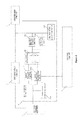
- FIG. 1 is a block diagram illustrating a first conventional UPS.
- the UPS includes an input filtering circuit 1, a rectification circuit 2, an inversion circuit 3, a static transfer switch 4, an output filtering circuit 5, a control circuit 6, an auxiliary circuit 7, an DC/DC circuit A, a rechargeable battery B and a charging circuit C.
- the input filtering circuit 1, the rectification circuit 2, the inversion circuit 3, the static transfer switch 4 and the output filtering circuit 5 are connected sequentially; and the output terminal of the input filtering circuit 1 is connected with the input terminal of the static transfer switch 4.
- the charging circuit C is connected between the rechargeable battery B and the output terminal of the input filtering circuit 1.
- the DC/DC circuit A is connected between the rechargeable battery B and the output terminal of the rectification circuit 2.
- the DC/DC circuit A, the rectification circuit 2, the inversion circuit 3 and the static transfer switch 4 are all controlled by the control circuit 6.
- the rechargeable battery B powers the auxiliary circuit 7.
- the rechargeable battery B In a mains power mode of the UPS, the rechargeable battery B is charged, by the mains power via the input filtering circuit 1 and then the charging circuit C.
- the rechargeable battery B is discharged, via the DC/DC circuit A to supply an input voltage to the inversion circuit 3.
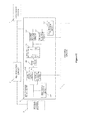
- FIG. 2 is a block diagram illustrating a second conventional UPS.
- the second UPS differs from the first UPS in that: the charging circuit C is connected between the rechargeable battery B and the output terminal of the rectification circuit 2.
- the rechargeable battery B is charged, by the mains power via the input filtering circuit 1, the rectification circuit 2 and then the charging circuit C; in a battery mode of the UPS, the rechargeable battery B is discharged, via the DC/DC circuit A to supply an input voltage to the inversion circuit 3.
- the rechargeable battery B is charged using an independent charging circuit C, causing a complex circuit structure and a higher cost.
- a technical problem to be solved by the present invention is to provide a UPS control circuit and a UPS.
- a UPS control circuit connected with a rechargeable battery including an input filtering circuit, a rectification circuit, an inversion circuit, a static transfer switch, an output filtering circuit, a control circuit, and an auxiliary circuit, the input filtering circuit, the rectification circuit, the inversion circuit, the static transfer switch, and the output filtering circuit being connected sequentially, an output terminal of the input filtering circuit being connected with an input terminal of the static transfer switch, and the rectification circuit, the inversion circuit, and the static transfer switch all being controlled by the control circuit
- the control circuit further includes a multipurpose DC/DC circuit connected between an output terminal of the rectification circuit and the rechargeable battery, and the multipurpose DC/DC circuit is controlled by the control circuit, so that in a battery mode, the rechargeable battery supplies an input voltage to the inversion circuit via the multipurpose DC/DC circuit; and in a mains power mode, the rechargeable battery is charged by an output voltage of the rectification circuit via the multipurpose DC
- the multipurpose DC/DC circuit may include a battery/mains power selector switch and an isolation transformer, a primary side of the isolation transformer is provided with a first switching transistor group, a first rectification circuit, and a first filter capacitor group, and a secondary side of the isolation transformer is provided with a second switching transistor group, a second rectification circuit, and a second filter capacitor group,
- the battery/mains power selector switch is a manually-operated switch, or an electrically-operated switch controlled by the control circuit, when the battery mode is selected by the battery/mains power selector switch, the control circuit controls the first switching transistor group to be rapidly switched between on and off, so that an output voltage of the rechargeable battery is converted into a first AC voltage, which is applied to the primary side of the isolation transformer, resulting in a second AC voltage on the secondary side of the isolation transformer; at the same time, the control circuit controls the second switching transistor group to be turned off, so that the second AC voltage is converted into a DC voltage via the second
- the first switching transistor group may include a first switching transistor and a second switching transistor, each of the first switching transistor and the second switching transistor includes a body diode, the first rectification circuit is a half-wave rectification circuit formed by the body diode of the first switching transistor and the body diode of the second switching transistor, the first filter capacitor group may include a first capacitor, the second switching transistor group may include a third switching transistor and a fourth switching transistor, the second rectification circuit may be a bridge rectifier, and the second filter capacitor group may include a third capacitor and a fourth capacitor, an anode of the rechargeable battery is connected to a center tap of the primary winding of the isolation transformer via the battery/mains power selector switch, a cathode of the rechargeable battery is connected to a dotted terminal of the primary winding of the isolation transformer via the first switching transistor, and is connected to a non-dotted terminal of the primary winding of the isolation transformer via the second switching transistor, and the first capacitor is connected between
- the second switching transistor group may further include a fifth switching transistor and a sixth switching transistor, and the positive output terminal of the bridge rectifier is connected to the negative output terminal of the bridge rectifier via the fifth switching transistor and the sixth switching transistor, with an intersection of the fifth switching transistor and the sixth switching transistor connected to the non-dotted terminal of the secondary winding of the isolation transformer.
- the multipurpose DC/DC circuit may include an isolation transformer, a primary side of the isolation transformer is provided with a first switching transistor group, a first rectification circuit, and a first filter capacitor group, and a secondary side of the isolation transformer is provided with a second switching transistor group, a second rectification circuit, and a second filter capacitor group, in the battery mode, the control circuit controls the first switching transistor group to be rapidly switched between on and off, so that an output voltage of the rechargeable battery is converted into a first AC voltage, which is applied to the primary side of the isolation transformer, resulting in a second AC voltage on the secondary side of the isolation transformer; at the same time, the control circuit controls the second switching transistor group to be turned off, so that the second AC voltage is converted into a DC voltage via the second rectification circuit and the second filter capacitor group, to supply an input voltage to the inversion circuit; and in the mains power mode, the control circuit controls the second switching transistor group to be rapidly switched between on and off, so that an output voltage of the
- the first switching transistor group may include a first switching transistor, a second switching transistor, a third switching transistor, and a fourth switching transistor, each of the first switching transistor, the second switching transistor, the third switching transistor, and the fourth switching transistor includes a body diode
- the first rectification circuit is a full-wave rectification circuit formed by the body diode of the first switching transistor, the body diode of the second switching transistor, the body diode of the third switching transistor, and the body diode of the fourth switching transistor
- the first filter capacitor group may include a first capacitor
- the second switching transistor group may include a fifth switching transistor and a sixth switching transistor
- the second rectification circuit may be a bridge rectifier
- the second filter capacitor group may include a third capacitor and a fourth capacitor
- an anode of the rechargeable battery is connected to a cathode of the rechargeable battery via the first switching transistor and the second switching transistor, and the anode of the rechargeable battery is also connected to the cathode of the
- the second switching transistor group may further include a seventh switching transistor and an eighth switching transistor, and the positive output terminal of the bridge rectifier is connected to the negative output terminal of the bridge rectifier via the seventh switching transistor and the eighth switching transistor, with an intersection of the seventh switching transistor and the eighth switching transistor connected to the non-dotted terminal of the secondary winding of the isolation transformer.
- the multipurpose DC/DC circuit may include an isolation transformer, a primary side of the isolation transformer is provided with a first switching transistor group, a first rectification circuit, a first filter capacitor group, and a resonant circuit, and a secondary side of the isolation transformer is provided with a second switching transistor group, a second rectification circuit, and a second filter capacitor group, in the battery mode, the control circuit controls the first switching transistor group to be rapidly switched between on and off, so that an output voltage of the rechargeable battery is converted via the resonant circuit into a first AC voltage, which is applied to the primary side of the isolation transformer, resulting in a second AC voltage on the secondary side of the isolation transformer; at the same time, the control circuit controls the second switching transistor group to be turned off, so that the second AC voltage is converted into a DC voltage via the second rectification circuit and the second filter capacitor group, to supply an input voltage to the inversion circuit, and in the mains power mode, the control circuit controls the second switching transistor group to
- the first switching transistor group may include a first switching transistor, a second switching transistor, a third switching transistor, and a fourth switching transistor
- the first filter capacitor group may include a first capacitor
- the first rectification circuit may include a charging capacitor and an induction coil
- the second switching transistor group may include a fifth switching transistor and a sixth switching transistor
- the second rectification circuit may be a bridge rectifier
- the second filter capacitor group may include a third capacitor and a fourth capacitor
- an anode of the rechargeable battery is connected to a cathode of the rechargeable battery via the first switching transistor and the second switching transistor
- the anode of the rechargeable battery is also connected to the cathode of the rechargeable battery via the third switching transistor and the fourth switching transistor, with an intersection of the first switching transistor and the second switching transistor connected to a dotted terminal of the primary winding of the isolation transformer via the charging capacitor and then the induction coil, and an intersection of the third switching transistor and the fourth switching transistor connected to a non-dotted terminal
- a UPS including a rechargeable battery and a UPS control circuit connected with the rechargeable battery, the UPS control circuit being any one of the above UPS control circuits.
- a multipurpose DC/DC circuit is connected between an output terminal of a rectification circuit 2 and a rechargeable battery B, so that in a mains power mode, the rechargeable battery is charged by the mains power via an input filtering circuit, the rectification circuit, and the multipurpose DC/DC circuit; and in a battery mode, the rechargeable battery supplies an input voltage to an inversion circuit via the multipurpose DC/DC circuit. Therefore, the multipurpose DC/DC circuit incorporates the charging and discharging functions, eliminating the need for an independent charging circuit to charge the rechargeable battery, resulting in a simpler circuit structure and a lower cost, and providing greater value to the customer.
- FIG. 1 is a block diagram illustrating a first conventional UPS
- FIG. 2 is a block diagram illustrating a second conventional UPS
- FIG. 3 is a block diagram illustrating a UPS according to the present invention.
- FIG. 4 is a block diagram illustrating a multipurpose DC/DC circuit according to a first embodiment of the present invention
- FIG. 5 is a circuit diagram illustrating a first preferred embodiment of FIG. 4 ;
- FIG. 6 is a circuit diagram illustrating a second preferred embodiment of FIG. 4 ;
- FIG. 7 is a circuit diagram illustrating a third preferred embodiment of FIG. 4 ;
- FIG. 8 is a block diagram illustrating a multipurpose DC/DC circuit according to a second embodiment of the present invention.
- FIG. 9 is a circuit diagram illustrating a first preferred embodiment of FIG. 8 ;
- FIG. 10 is a circuit diagram illustrating a second preferred embodiment of FIG. 8 ;
- FIG. 11 is a circuit diagram illustrating a third preferred embodiment of FIG. 8 ;
- FIG. 12 is a block diagram illustrating a multipurpose DC/DC circuit according to a third embodiment of the present invention.
- FIG. 13 is a circuit diagram illustrating a first preferred embodiment of FIG. 12 ;
- FIG. 14 is a circuit diagram illustrating a second preferred embodiment of FIG. 12 .
- FIG. 15 is a circuit diagram illustrating a third preferred embodiment of FIG. 12 .
- FIG. 3 is a block diagram illustrating a UPS according to the present invention.
- the UPS includes a rechargeable battery B and a UPS control circuit connected with the rechargeable battery B.
- the UPS control circuit includes an input filtering circuit 1, a rectification circuit 2, an inversion circuit 3, a static transfer switch 4, an output filtering circuit 5, a control circuit 6, and a multipurpose DC/DC circuit 8.
- the input filtering circuit 1, the rectification circuit 2, the inversion circuit 3, the static transfer switch 4, and the output filtering circuit 5 are connected sequentially, and an output terminal of the input filtering circuit 1 is connected with an input terminal of the static transfer switch 4.
- the rectification circuit 2, the inversion circuit 3, the static transfer switch 4, and the multipurpose DC/DC circuit 8 are all connected with and controlled by the control circuit 6.
- the multipurpose DC/DC circuit is connected between the output terminal of the rectification circuit 2 and the rechargeable battery B.
- the rechargeable battery supplies an input voltage to the inversion circuit 3 via the multipurpose DC/DC circuit 8.
- the rechargeable battery B is charged by an output voltage of the rectification circuit 2 via the multipurpose DC/DC circuit 8.
- the multipurpose DC/DC circuit 8 is connected between the output terminal of the rectification circuit 2 and the rechargeable battery B, and the multipurpose DC/DC circuit A is connected with and controlled by the control circuit 6.
- the rechargeable battery In the battery mode, the rechargeable battery is charged by the mains power via the input filtering circuit 1, the rectification circuit 2, and the multipurpose DC/DC circuit 8.
- the rechargeable battery In the mains power mode, the rechargeable battery supplies an input voltage to the inversion circuit 3 via the multipurpose DC/DC circuit 8.
- the multipurpose DC/DC circuit 8 incorporates the charging and discharging functions, eliminating the need for an independent charging circuit to charge the rechargeable battery B, resulting in a simpler circuit structure and a lower cost of the UPS control circuit, and providing greater value to the customer.
- the UPS according to the embodiment of the present invention may further include an auxiliary circuit 7 arranged between the multipurpose DC/DC circuit 8 and the rechargeable battery B.
- FIG. 4 is a block diagram illustrating a multipurpose DC/DC circuit according to a first embodiment of the present invention.
- the multipurpose DC/DC circuit 8 includes a battery/mains power selector switch 100 and an isolation transformer 101.
- a primary side of the isolation transformer 101 is provided with a first switching transistor group 103, a first rectification circuit 102, and a first filter capacitor group 104.
- a secondary side of the isolation transformer 101 is provided with a second switching transistor group 106, a second rectification circuit 105, and a second filter capacitor group 107.
- the first switching transistor group 103 and the second switching transistor group 106 are all controlled by the control circuit 6.
- the output terminal of the rechargeable battery B is connected to the primary side of the isolation transformer 101 via the battery/mains power selector switch 100 and then the first rectification circuit 102. Meanwhile, the output terminal of the rechargeable battery B is also connected to the primary side of the isolation transformer 101 via the battery/mains power selector switch 100 and then the first switching transistor group 103. Moreover, the first filter capacitor group 104 is connected to the output terminal of the battery/mains power selector switch 100 (i.e., the intersection between the battery/mains power selector switch 100 and the first rectification circuit 102). The secondary side of the isolation transformer 101 is connected to the input terminal of a conversion circuit 3 (i.e., the inversion circuit 3 in Figure 3 ) via the second rectification circuit 105. Meanwhile, the secondary side of the isolation transformer 101 is also connected to the input terminal of the conversion circuit 3 via the second switching transistor group 106. The second filter capacitor group 107 is connected to the input terminal of the conversion circuit 3.
- a conversion circuit 3 i.e., the inversion circuit 3
- the control circuit 6 controls the first switching transistor group 103 to be rapidly switched between on and off, so that an output voltage of the rechargeable battery B is converted into a first AC voltage, which is applied to the primary side of the isolation transformer 101, resulting in a second AC voltage on the secondary side of the isolation transformer 101.
- the control circuit 6 controls the second switching transistor group 106 to be turned off, so that the second AC voltage is converted into a DC voltage via the second rectification circuit 105 and the second filter capacitor group 107, to supply an input voltage to the conversion circuit 3.
- the control circuit 6 controls the second switching transistor group 106 to be rapidly switched between on and off, so that an output voltage of the rectification circuit 2 is converted into a third AC voltage, which is applied to the secondary side of the isolation transformer 101, resulting in a fourth AC voltage on the primary side of the isolation transformer 101.
- the fourth AC voltage is converted into a DC voltage via the first rectification circuit 102 and the first filter capacitor group 104, to charge the rechargeable battery B.
- the battery/mains power selector switch 100 may be a manually-operated switch, or an electrically-operated switch controlled by the control circuit 6.
- FIG. 5 is a circuit diagram illustrating a first preferred embodiment of FIG. 4 .
- the first switching transistor group 103 includes a first switching transistor Q1 and a second switching transistor Q2.
- Each of the first switching transistor Q1 and the second switching transistor Q2 includes a body diode.
- the first rectification circuit 102 is a half-wave rectification circuit formed by the body diode of the first switching transistor Q1 and the body diode of the second switching transistor Q2.
- the first filter capacitor group 104 includes a first capacitor C1.
- the second switching transistor group 106 includes a third switching transistor Q3 and a fourth switching transistor Q4.
- the second rectification circuit 105 is a bridge rectifier D.
- the second filter capacitor group 107 includes a third capacitor C3 and a fourth capacitor C4.
- the anode of the rechargeable battery B is connected to a center tap of the primary winding of the isolation transformer 101 via the battery/mains power selector switch 100.
- the cathode of the rechargeable battery B is connected to a dotted terminal of the primary winding of the isolation transformer 101 via the first switching transistor Q1, and is connected to a non-dotted terminal of the primary winding of the isolation transformer 101 via the second switching transistor Q2.
- the first capacitor C1 is connected between the center tap of the primary winding of isolation transformer 101 and the cathode of the rechargeable battery B.
- a first diode D1 is arranged between the center tap of the primary winding of the isolation transformer 101 and the anode of the rechargeable battery B.
- the anode of the first diode D1 is connected with the center tap of the primary winding of the isolation transformer 101, and the cathode of the first diode D1 is connected with the anode of the rechargeable battery B.
- the battery/mains power selector switch 100 When the mains power mode is selected by the battery/mains power selector switch 100, the battery/mains power selector switch 100 is open, and the rechargeable battery B is charged by a charging current via the first diode D1, thereby preventing ripple which may affect the rechargeable battery B.
- a dotted terminal of the secondary winding of the isolation transformer 101 is connected to a positive input terminal I+ of the bridge rectifier D.
- a non-dotted terminal of the secondary winding of the isolation transformer 101 is connected to a negative input terminal I- of the bridge rectifier D.
- a positive output terminal O+ of the bridge rectifier D is connected to a negative output terminal O- of the bridge rectifier D via the third switching transistor Q3 and then the fourth switching transistor Q4, with an intersection of the third switching transistor Q3 and the fourth switching transistor Q4 connected to the non-dotted terminal of the secondary winding of the isolation transformer 101.
- the positive output terminal O+ of the bridge rectifier D is also connected to the negative output terminal O- of the bridge rectifier D via the third capacitor C3 and then the fourth capacitor C4, with an intersection of the third capacitor C3 and the fourth capacitor C4 connected to a center tap of the secondary winding of the isolation transformer 101.
- the battery mode is selected when the battery/mains power selector switch 100 is closed.
- the mains power mode is selected when the battery/mains power selector switch 100 is open.
- FIG. 6 is a circuit diagram illustrating a second preferred embodiment of FIG. 4 .
- the second preferred embodiment differs from the first embodiment shown in Figure 5 in that:
- the intersection of the third switching transistor Q3 and the fourth switching transistor Q4 is connected to the dotted terminal of the secondary winding of the isolation transformer 101.
- FIG. 7 is a circuit diagram illustrating a third preferred embodiment of FIG. 4 .
- the third preferred embodiment differs from the second embodiment shown in Figure 6 in that: the second switching transistor group 106 further includes a fifth switching transistor Q5 and a sixth switching transistor Q6.
- the positive output terminal O+ of the bridge rectifier D is connected to the negative output terminal Q- of the bridge rectifier D via the fifth switching transistor Q5 and then the sixth switching transistor Q6, with an intersection of the fifth switching transistor Q5 and the sixth switching transistor Q6 connected to the non-dotted terminal of the secondary winding of the isolation transformer 101.
- FIG. 8 is a block diagram illustrating a multipurpose DC/DC circuit according to a second embodiment of the present invention.
- the multipurpose DC/DC circuit 8 includes an isolation transformer 101.
- a primary side of the isolation transformer 101 is provided with a first switching transistor group 103, a first rectification circuit 102, and a first filter capacitor group 104.
- a secondary side of the isolation transformer 101 is provided with a second switching transistor group 106, a second rectification circuit 105, and a second filter capacitor group 107.
- the output terminal of the rechargeable battery B is connected to the primary side of the isolation transformer 101 via the first rectification circuit 102.
- the output terminal of the rechargeable battery B is also connected to the primary side of the isolation transformer 101 via the first switching transistor group 103.
- the first filter capacitor group 104 is connected to the output terminal of the rechargeable battery B.
- the secondary side of the isolation transformer 101 is connected to the input terminal of the conversion circuit 3 via the second rectification circuit 105. Meanwhile, the secondary side of the isolation transformer 101 is also connected to the input terminal of the conversion circuit 3 via the second switching transistor group 106.
- the second filter capacitor group 107 is connected to the input terminal of the conversion circuit 3.
- the control circuit 6 controls the first switching transistor group 103 to be rapidly switched between on and off, so that an output voltage of the rechargeable battery B is converted via the first rectification circuit 102 into a first AC voltage, which is applied to the primary side of the isolation transformer 101, resulting in a second AC voltage on the secondary side of the isolation transformer 101.
- the control circuit 6 controls the second switching transistor group 106 to be turned off, so that the second AC voltage is converted into a DC voltage via the second rectification circuit 105 and the second filter capacitor group 107, to supply an input voltage to the conversion circuit 3.
- the control circuit 6 controls the second switching transistor group 106 to be rapidly switched between on and off, so that an output voltage of the rectification circuit 2 is converted into a third AC voltage, which is applied to the secondary side of the isolation transformer 101, resulting in a fourth AC voltage on the primary side of the isolation transformer 101.
- the fourth AC voltage is converted into a DC voltage via the first rectification circuit 104 and the first filter capacitor group 102, to charge the rechargeable battery B.
- control circuit 6 may automatically detect whether the mains power is in a normal state, and charge the rechargeable battery B with the mains power when the mains power is normal; and initiate the UPS to power the load in a battery mode when the mains power fails.
- control circuit 6 may monitor the charge stored in the rechargeable battery B, in order to prevent overcharging and overdischarging.
- FIG. 9 is a circuit diagram illustrating a first preferred embodiment of FIG. 8 .
- the first switching transistor group 103 includes a first switching transistor Q1, a second switching transistor Q2, a third switching transistor Q3, and a fourth switching transistor Q4.
- the first rectification circuit 102 is a full-wave rectification circuit formed by the body diode of the first switching transistor Q1, the body diode of the second switching transistor Q2, the body diode of the third switching transistor Q3, and the body diode of the fourth switching transistor Q4.
- the first filter capacitor group 104 includes a first capacitor C1.
- the second switching transistor group 106 includes a fifth switching transistor Q5 and a sixth switching transistor Q6.
- the second rectification circuit 105 is a bridge rectifier D.
- the second filter capacitor group 107 includes a third capacitor C3 and a fourth capacitor C4.
- the anode of the rechargeable battery B is connected to the cathode of the rechargeable battery B via the first switching transistor Q1 and the second switching transistor Q2.
- the anode of the rechargeable battery B is also connected to the cathode of the rechargeable battery B via the third switching transistor Q3 and the fourth switching transistor Q4.
- An intersection of the first switching transistor Q1 and the second switching transistor Q2 is connected to a dotted terminal of the primary winding of the isolation transformer 101.
- An intersection of the third switching transistor Q3 and the fourth switching transistor Q4 is connected to a non-dotted terminal of the primary winding of the isolation transformer 101.
- the first capacitor C1 is connected between the anode and the cathode of the rechargeable battery B.
- a dotted terminal of the secondary winding of the isolation transformer 101 is connected to a positive input terminal I+ of the bridge rectifier D.
- a non-dotted terminal of the secondary winding of the isolation transformer 101 is connected to a negative input terminal I- of the bridge rectifier D.
- a positive output terminal O+ of the bridge rectifier D is connected to a negative output terminal O- of the bridge rectifier D via the fifth switching transistor Q5 and then the sixth switching transistor Q6, with an intersection of the fifth switching transistor Q5 and the sixth switching transistor Q6 connected to the non-dotted terminal of the secondary winding of the isolation transformer 101.
- the positive output terminal O+ of the bridge rectifier D is connected to the negative output terminal O- of the bridge rectifier D via the third capacitor C3 and then the fourth capacitor C4, with an intersection of the third capacitor C3 and the fourth capacitor C4 connected to a center tap of the secondary winding of the isolation transformer 101.
- FIG. 10 is a circuit diagram illustrating a second preferred embodiment of FIG. 8 .
- the second preferred embodiment differs from the first preferred embodiment shown in Figure 9 in that: the intersection of the fifth switching transistor Q5 and the sixth switching transistor Q6 is connected to the dotted terminal of the secondary winding of the isolation transformer 101.
- FIG. 11 is a circuit diagram illustrating a third preferred embodiment of FIG. 8 .
- the third preferred embodiment differs from the second embodiment shown in Figure 10 in that: the second switching transistor group 106 further includes a seventh switching transistor Q7 and an eighth switching transistor Q8.
- the positive output terminal O+ of the bridge rectifier D is connected to the negative output terminal Q- of the bridge rectifier D via the seventh switching transistor Q7 and then the eighth switching transistor Q8, with an intersection of the seventh switching transistor Q7 and the eighth switching transistor Q8 connected to the non-dotted terminal of the secondary winding of the isolation transformer 101.
- FIG. 12 is a block diagram illustrating a multipurpose DC/DC circuit according to a third embodiment of the present invention.
- the multipurpose DC/DC circuit 8 includes an isolation transformer 101.
- a primary side of the isolation transformer 101 is provided with a first switching transistor group 103, a first filter capacitor group 104, a first rectification circuit 102, and a resonant circuit 108.
- a secondary side of the isolation transformer 101 is provided with a second switching transistor group 106, a second rectification circuit 105, and a second filter capacitor group 107.
- the output terminal of the rechargeable battery B is connected to the primary side of the isolation transformer 101 via the first rectification circuit 102 and the resonant circuit 108. Meanwhile, the output terminal of the rechargeable battery B is also connected to the primary side of the isolation transformer 101 via the first switching transistor group 103 and the resonant circuit 108.
- the first filter capacitor group 104 is connected to the output terminal of the rechargeable battery B.
- the secondary side of the isolation transformer 101 is connected to the input terminal of the conversion circuit 3 via the second rectification circuit 105. Meanwhile, the secondary side of the isolation transformer 101 is also connected to the input terminal of the conversion circuit 3 via the second switching transistor group 106.
- the second filter capacitor group 107 is connected to the input terminal of the conversion circuit 3.
- the control circuit 6 controls the first switching transistor group 103 to be rapidly switched between on and off, so that an output voltage of the rechargeable battery B is converted via the resonant circuit 108 into a first AC voltage, which is applied to the primary side of the isolation transformer 101, resulting in a second AC voltage on the secondary side of the isolation transformer 101.
- the control circuit 6 controls the second switching transistor group 106 to be turned off, so that the second AC voltage is converted into a DC voltage via the second rectification circuit 105 and the second filter capacitor group 107, to supply an input voltage to the inversion circuit 3.
- the control circuit 6 controls the second switching transistor group 106 to be rapidly switched between on and off, so that an output voltage of the rectification circuit 2 is converted into a third AC voltage, which is applied to the secondary side of the isolation transformer 101, resulting in a fourth AC voltage on the primary side of the isolation transformer 101.
- the fourth AC voltage is converted into a DC voltage via the resonant circuit 108, the first rectification circuit 102 and the first filter capacitor group 104, to charge the rechargeable battery B.
- the resonant circuit 108 can improve the power factor.
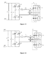
- FIG. 13 is a circuit diagram illustrating a first preferred embodiment of FIG. 12 .
- the first switching transistor group 103 includes a first switching transistor Q1, a second switching transistor Q2, a third switching transistor Q3, and a fourth switching transistor Q4.
- the first rectification circuit 102 is a full-wave rectification circuit formed by the body diode of the first switching transistor Q1, the body diode of the second switching transistor Q2, the body diode of the third switching transistor Q3, and the body diode of the fourth switching transistor Q4.
- the first filter capacitor group 104 includes a first capacitor C1.
- the resonant circuit 108 includes a charging capacitor Cc and an induction coil L1.
- the second switching transistor group 106 includes a fifth switching transistor Q5 and a sixth switching transistor Q6.
- the second rectification circuit 102 is a bridge rectifier D.
- the second filter capacitor group 107 includes a third capacitor C3 and a fourth capacitor C4.
- the anode of the rechargeable battery B is connected to the cathode of the rechargeable battery B via the first switching transistor Q1 and the second switching transistor Q2.
- the anode of the rechargeable battery B is also connected to the cathode of the rechargeable battery B via the third switching transistor Q3 and the fourth switching transistor Q4.
- An intersection of the first switching transistor Q1 and the second switching transistor Q2 is connected to a dotted terminal of the primary winding of the isolation transformer 101 via the charging capacitor Cc and then the induction coil L1.
- An intersection of the third switching transistor Q3 and the fourth switching transistor Q4 is connected to a non-dotted terminal of the primary winding of the isolation transformer 101.
- the first capacitor C1 is connected between the anode and the cathode of the rechargeable battery B.
- a dotted terminal of the secondary winding of the isolation transformer 101 is connected to a positive input terminal I+ of the bridge rectifier D.
- a non-dotted terminal of the secondary winding of the isolation transformer 101 is connected to a negative input terminal I- of the bridge rectifier D.
- a positive output terminal O+ of the bridge rectifier D is connected to a negative output terminal O- of the bridge rectifier D via the fifth switching transistor Q5 and then the sixth switching transistor Q6, with an intersection of the fifth switching transistor Q5 and the sixth switching transistor Q6 connected to the non-dotted terminal of the secondary winding of the isolation transformer 101.
- the positive output terminal O+ of the bridge rectifier D is connected to the negative output terminal O- of the bridge rectifier D via the third capacitor C3 and then the fourth capacitor C4, with an intersection of the third capacitor C3 and the fourth capacitor C4 connected to a center tap of the secondary winding of the isolation transformer 101.
- FIG. 14 is a circuit diagram illustrating a second preferred embodiment of FIG. 12 .
- the second preferred embodiment differs from the first preferred embodiment shown in Figure 13 in that:
- the intersection of the fifth switching transistor Q5 and the sixth switching transistor Q6 is connected to the dotted terminal of the secondary winding of the isolation transformer 101.
- FIG. 15 is a circuit diagram illustrating a third preferred embodiment of FIG. 12 .
- the third preferred embodiment differs from the first preferred embodiment shown in Figure 14 in that: the second switching transistor group 106 further includes a seventh switching transistor Q7 and an eighth switching transistor Q8.
- the positive output terminal O+ of the bridge rectifier D is connected to the negative output terminal Q- of the bridge rectifier D via the seventh switching transistor Q7 and then the eighth switching transistor Q8, with an intersection of the seventh switching transistor Q7 and the eighth switching transistor Q8 connected to the non-dotted terminal of the secondary winding of the isolation transformer 101.
- any one or more of the first switching transistor Q1, the second switching transistor Q2,..., and the eighth switching transistor Q8 may be an IGBT, or a MOSFET, or any other switching transistor.
- the control circuit 6 can adjust charging and discharging voltage/current by adjusting duty cycles of switching on/off of those switching transistors.
- the present invention also provides a UPS including a rechargeable battery B and a UPS control circuit connected with the rechargeable battery.
- the UPS control circuit may be any one of the above UPS control circuits, the details of which are omitted here.
Landscapes
- Engineering & Computer Science (AREA)
- Power Engineering (AREA)
- Business, Economics & Management (AREA)
- Emergency Management (AREA)
- Charge And Discharge Circuits For Batteries Or The Like (AREA)
- Dc-Dc Converters (AREA)
Applications Claiming Priority (2)
| Application Number | Priority Date | Filing Date | Title |
|---|---|---|---|
| CN2010105206534A CN101976871B (zh) | 2010-10-22 | 2010-10-22 | 一种ups电源控制电路和ups电源 |
| PCT/CN2011/080980 WO2012051945A1 (fr) | 2010-10-22 | 2011-10-19 | Circuit de commande d'alimentation électrique sans coupure et alimentation électrique sans coupure associée |
Publications (2)
| Publication Number | Publication Date |
|---|---|
| EP2632015A1 true EP2632015A1 (fr) | 2013-08-28 |
| EP2632015A4 EP2632015A4 (fr) | 2016-11-30 |
Family
ID=43576728
Family Applications (1)
| Application Number | Title | Priority Date | Filing Date |
|---|---|---|---|
| EP11833851.6A Withdrawn EP2632015A4 (fr) | 2010-10-22 | 2011-10-19 | Circuit de commande d'alimentation électrique sans coupure et alimentation électrique sans coupure associée |
Country Status (4)
| Country | Link |
|---|---|
| US (1) | US9570930B2 (fr) |
| EP (1) | EP2632015A4 (fr) |
| CN (1) | CN101976871B (fr) |
| WO (1) | WO2012051945A1 (fr) |
Cited By (2)
| Publication number | Priority date | Publication date | Assignee | Title |
|---|---|---|---|---|
| WO2020176073A1 (fr) * | 2019-02-25 | 2020-09-03 | Hewlett-Packard Development Company, L.P. | Stockage d'énergie et combinateurs de puissance à courant alternatif |
| CN114312392A (zh) * | 2020-09-30 | 2022-04-12 | 比亚迪股份有限公司 | 车辆充电装置、方法及车辆 |
Families Citing this family (27)
| Publication number | Priority date | Publication date | Assignee | Title |
|---|---|---|---|---|
| CN101976871B (zh) * | 2010-10-22 | 2013-03-06 | 艾默生网络能源有限公司 | 一种ups电源控制电路和ups电源 |
| CN103187876B (zh) * | 2011-12-28 | 2016-08-03 | 艾默生网络能源有限公司 | 一种不间断电源的dc/dc电路 |
| CN103715746B (zh) * | 2012-09-29 | 2016-08-24 | 艾默生网络能源有限公司 | 一种ups及其dc/dc电路 |
| CN103368249B (zh) * | 2012-03-26 | 2016-02-10 | 阿里巴巴集团控股有限公司 | 一种不间断电源供电的系统和方法 |
| CN102638093B (zh) * | 2012-04-27 | 2015-04-01 | 天津三星电子有限公司 | 一种断电保护装置 |
| AT512887B1 (de) * | 2012-04-27 | 2014-03-15 | Siemens Ag | Ausgangsstufe eines Ladegerätes |
| CN104810871B (zh) * | 2014-01-26 | 2018-12-11 | 伊顿制造(格拉斯哥)有限合伙莫尔日分支机构 | 不间断电源及其启动方法 |
| CN105024551A (zh) * | 2014-04-16 | 2015-11-04 | 艾默生网络能源有限公司 | 一种谐振电路、充电器及不间断电源 |
| CN106663945A (zh) * | 2014-08-22 | 2017-05-10 | 东宾制造有限公司 | 对多个电池组的控制 |
| CN104505878A (zh) * | 2014-12-12 | 2015-04-08 | 国家电网公司 | 一种便携式稳压移动电源装置 |
| EP3411933A1 (fr) * | 2016-02-02 | 2018-12-12 | Koninklijke Philips N.V. | Appareil de distribution de puissance multifonctionnel |
| CN106339060A (zh) * | 2016-08-30 | 2017-01-18 | 成都英格瑞德电气有限公司 | 一种基于触摸屏控制的ups系统 |
| CN106253462A (zh) * | 2016-08-30 | 2016-12-21 | 成都英格瑞德电气有限公司 | 具有滤波功能的改进ups系统 |
| CN107026503B (zh) * | 2017-03-28 | 2020-07-10 | 湖北航天技术研究院总体设计所 | 一种火箭发射车柔性不间断直流电源系统的控制方法 |
| CN108808833A (zh) * | 2017-05-24 | 2018-11-13 | 伊顿制造(格拉斯哥)有限合伙莫尔日分支机构 | 一种ups电路 |
| CN107650729B (zh) * | 2017-10-26 | 2019-06-04 | 科博达技术股份有限公司 | 新能源汽车的高压电器的预充电装置 |
| CN109245283B (zh) * | 2018-10-16 | 2023-12-29 | 深圳市科陆电子科技股份有限公司 | 备用电池监控系统及不间断供电智能切换及监控系统 |
| CN110165773A (zh) * | 2019-04-29 | 2019-08-23 | 浙江大邦科技有限公司 | 基于智慧路灯的不间断供电系统 |
| CN110061560B (zh) * | 2019-05-24 | 2022-02-08 | 联正电子(深圳)有限公司 | 离线式不间断电源及其控制方法 |
| CN110061559B (zh) * | 2019-05-24 | 2022-01-25 | 联正电子(深圳)有限公司 | 离线式不间断电源及其控制方法 |
| CN110425174B (zh) * | 2019-07-24 | 2024-07-26 | 许继电源有限公司 | 风机调速电路、多路并联风机调速电路 |
| CN110601327A (zh) * | 2019-10-14 | 2019-12-20 | 美平电器制品(深圳)有限公司 | 一种混能美发器 |
| CN110696672B (zh) * | 2019-11-08 | 2023-04-11 | 成都信息工程大学 | 一种实现动力电池快速充电的系统 |
| CN112803610B (zh) * | 2019-11-14 | 2024-07-09 | Oppo广东移动通信有限公司 | 待充电设备、系统以及无线充电方法、存储介质 |
| CN113078728A (zh) * | 2021-05-06 | 2021-07-06 | 深圳弘德智能有限公司 | 一种单相安全高频隔离ups电源 |
| CN117656892B (zh) * | 2022-08-30 | 2024-10-29 | 比亚迪股份有限公司 | 车辆供电系统及车辆 |
| CN116692621A (zh) * | 2023-06-19 | 2023-09-05 | 日立楼宇技术(广州)有限公司 | 一种电梯制动器控制电路、电梯以及控制方法 |
Family Cites Families (19)
| Publication number | Priority date | Publication date | Assignee | Title |
|---|---|---|---|---|
| AU661564B2 (en) * | 1992-03-06 | 1995-07-27 | Hino Jidosha Kogyo Kabushiki Kaisha | Braking and auxiliary power apparatus of internal combustion engine |
| US5896280A (en) | 1997-11-25 | 1999-04-20 | Exide Electronics Corporation | Frequency converter and improved UPS employing the same |
| NZ332613A (en) | 1998-01-30 | 2000-06-23 | Silverline Power Conversion Ll | Uninterruptible power supply |
| US6115276A (en) | 1998-11-24 | 2000-09-05 | Lucent Technologies Inc. | AC bus system with battery charger/inverter backup |
| JP4191874B2 (ja) * | 2000-03-24 | 2008-12-03 | 株式会社高見沢サイバネティックス | 無停電電源装置 |
| CN2454974Y (zh) | 2000-11-02 | 2001-10-17 | 系统电子工业股份有限公司 | 自动调整不间断电源的侦测装置 |
| CN2572644Y (zh) * | 2002-03-14 | 2003-09-10 | 漳州市海峡科技实业有限公司 | 含ups功能的atx电源 |
| JP3908077B2 (ja) | 2002-04-16 | 2007-04-25 | 株式会社日立製作所 | 直流バックアップ電源装置とその診断方法 |
| US7352154B2 (en) * | 2004-01-14 | 2008-04-01 | Vanner, Inc. | Electrical system control for a vehicle |
| TWI332746B (en) * | 2006-04-17 | 2010-11-01 | Delta Electronics Inc | Low cost, low power loss ups device |
| WO2008007540A1 (fr) * | 2006-07-10 | 2008-01-17 | Panasonic Corporation | Dispositif d'alimentation |
| TWI324428B (en) * | 2007-03-28 | 2010-05-01 | Hybrid green uninterruptible power system and bi-directional converter module and power conversion method thereof | |
| US7796406B2 (en) * | 2007-07-31 | 2010-09-14 | Lumenis Ltd. | Apparatus and method for high efficiency isolated power converter |
| JP2009095071A (ja) | 2007-10-03 | 2009-04-30 | Tdk-Lambda Corp | 無停電電源装置 |
| JP4401418B2 (ja) * | 2008-04-18 | 2010-01-20 | シャープ株式会社 | 双方向dc/dcコンバータおよびパワーコンディショナ |
| US8102678B2 (en) | 2008-05-21 | 2012-01-24 | Flextronics Ap, Llc | High power factor isolated buck-type power factor correction converter |
| CN101685980B (zh) * | 2008-09-27 | 2012-11-14 | 力博特公司 | 一种用于ups的基于llc的全桥零电压开关升压谐振变换器 |
| CN101976871B (zh) * | 2010-10-22 | 2013-03-06 | 艾默生网络能源有限公司 | 一种ups电源控制电路和ups电源 |
| JP5559742B2 (ja) * | 2011-05-25 | 2014-07-23 | 日立建機株式会社 | 建設機械の電動駆動装置 |
-
2010
- 2010-10-22 CN CN2010105206534A patent/CN101976871B/zh active Active
-
2011
- 2011-10-19 EP EP11833851.6A patent/EP2632015A4/fr not_active Withdrawn
- 2011-10-19 WO PCT/CN2011/080980 patent/WO2012051945A1/fr not_active Ceased
- 2011-10-19 US US13/880,002 patent/US9570930B2/en not_active Expired - Fee Related
Cited By (2)
| Publication number | Priority date | Publication date | Assignee | Title |
|---|---|---|---|---|
| WO2020176073A1 (fr) * | 2019-02-25 | 2020-09-03 | Hewlett-Packard Development Company, L.P. | Stockage d'énergie et combinateurs de puissance à courant alternatif |
| CN114312392A (zh) * | 2020-09-30 | 2022-04-12 | 比亚迪股份有限公司 | 车辆充电装置、方法及车辆 |
Also Published As
| Publication number | Publication date |
|---|---|
| EP2632015A4 (fr) | 2016-11-30 |
| CN101976871B (zh) | 2013-03-06 |
| US9570930B2 (en) | 2017-02-14 |
| CN101976871A (zh) | 2011-02-16 |
| WO2012051945A1 (fr) | 2012-04-26 |
| US20130200708A1 (en) | 2013-08-08 |
Similar Documents
| Publication | Publication Date | Title |
|---|---|---|
| US9570930B2 (en) | UPS electricity supply control circuit and UPS electricity supply | |
| US10079541B1 (en) | Wide input, wide output, high efficiency, isolated DC-DC converter-battery charger | |
| TWI221695B (en) | Uninterruptible power system | |
| Hsieh et al. | A novel high step-up DC–DC converter for a microgrid system | |
| Zhang et al. | Flyback-based single-stage power-factor-correction scheme with time-multiplexing control | |
| TWI514734B (zh) | 電源適配器、電源適配器之控制方法及筆記型電腦 | |
| CN102742138B (zh) | Ac-dc转换器和ac-dc转换方法 | |
| US20200366215A1 (en) | Resonant Power Converters and Control Methods for Wide Input and Output Voltage Ranges | |
| EP2800230B1 (fr) | Circuit continu-continu pour alimentation électrique ininterruptible | |
| EP2662965A2 (fr) | Convertisseur de puissance résonant LLC avec circuit de circulation de courant permettant une régulation de charge légère | |
| EP3404816B1 (fr) | Système de convertisseur de puissance et procédé de fonctionnement d'un système de convertisseur de puissance | |
| CN103187876A (zh) | 一种不间断电源的dc/dc电路 | |
| EP2937979A1 (fr) | Source d'alimentation électrique de commutateur unipolaire | |
| US12132341B2 (en) | Battery charging and discharging circuit | |
| US12062943B2 (en) | AC switch PFC with integrated charger and DC-DC for online UPS systems | |
| JP6298634B2 (ja) | スイッチング電源装置 | |
| JP2014176226A (ja) | Dc/dc変換装置及び分散電源システム | |
| KR102691474B1 (ko) | 차량용 배터리 충전 제어 시스템 및 방법 | |
| US20230387815A1 (en) | Direct current to direct current converter, electronic device, and charger | |
| CN118523511A (zh) | 充电电路、电源电路、电子设备及供电系统 | |
| JP2014171313A (ja) | Dc/dcコンバータ | |
| Chen et al. | A new nonisolated three-port DC-DC converter with high step-up/down ratio | |
| RU2732280C1 (ru) | Источник бесперебойного питания - статический обратимый преобразователь для питания потребителей переменного и постоянного тока и заряда (подзаряда) аккумуляторной батареи | |
| Shafiei et al. | High power LLC battery charger: Wide regulation using phase-shift for recovery mode | |
| KR20020015465A (ko) | 무정전 스위칭 모드 전원 장치 |
Legal Events
| Date | Code | Title | Description |
|---|---|---|---|
| PUAI | Public reference made under article 153(3) epc to a published international application that has entered the european phase |
Free format text: ORIGINAL CODE: 0009012 |
|
| 17P | Request for examination filed |
Effective date: 20130514 |
|
| AK | Designated contracting states |
Kind code of ref document: A1 Designated state(s): AL AT BE BG CH CY CZ DE DK EE ES FI FR GB GR HR HU IE IS IT LI LT LU LV MC MK MT NL NO PL PT RO RS SE SI SK SM TR |
|
| DAX | Request for extension of the european patent (deleted) | ||
| RA4 | Supplementary search report drawn up and despatched (corrected) |
Effective date: 20161027 |
|
| RIC1 | Information provided on ipc code assigned before grant |
Ipc: H02J 7/02 20060101ALI20161021BHEP Ipc: H02J 7/00 20060101AFI20161021BHEP |
|
| RAP1 | Party data changed (applicant data changed or rights of an application transferred) |
Owner name: VERTIV TECH CO., LTD. |
|
| 17Q | First examination report despatched |
Effective date: 20180410 |
|
| STAA | Information on the status of an ep patent application or granted ep patent |
Free format text: STATUS: THE APPLICATION IS DEEMED TO BE WITHDRAWN |
|
| 18D | Application deemed to be withdrawn |
Effective date: 20190209 |