EP2632167B1 - Système permettant de détecter des pixels défectueux dans un réseau de capteurs - Google Patents
Système permettant de détecter des pixels défectueux dans un réseau de capteurs Download PDFInfo
- Publication number
- EP2632167B1 EP2632167B1 EP13156168.0A EP13156168A EP2632167B1 EP 2632167 B1 EP2632167 B1 EP 2632167B1 EP 13156168 A EP13156168 A EP 13156168A EP 2632167 B1 EP2632167 B1 EP 2632167B1
- Authority
- EP
- European Patent Office
- Prior art keywords
- optical
- intensity
- optical receiver
- radiation
- photosensitive
- Prior art date
- Legal status (The legal status is an assumption and is not a legal conclusion. Google has not performed a legal analysis and makes no representation as to the accuracy of the status listed.)
- Active
Links
Images

Classifications
-
- H—ELECTRICITY
- H04—ELECTRIC COMMUNICATION TECHNIQUE
- H04N—PICTORIAL COMMUNICATION, e.g. TELEVISION
- H04N17/00—Diagnosis, testing or measuring for television systems or their details
- H04N17/002—Diagnosis, testing or measuring for television systems or their details for television cameras
-
- H—ELECTRICITY
- H04—ELECTRIC COMMUNICATION TECHNIQUE
- H04N—PICTORIAL COMMUNICATION, e.g. TELEVISION
- H04N23/00—Cameras or camera modules comprising electronic image sensors; Control thereof
- H04N23/56—Cameras or camera modules comprising electronic image sensors; Control thereof provided with illuminating means
Definitions
- the subject matter disclosed herein relates to an optical sensor used in a safety system and, more specifically, to a system to test performance of the optical receiver used in the optical sensor.
- An optical sensor includes a receiver that converts light incident to the sensor into an electric signal.
- the receiver may include a single photosensitive device or an array of pixels, for example charge-coupled devices (CCD) or complementary metal-oxide-semiconductor (CMOS) sensors.
- CCD charge-coupled devices
- CMOS complementary metal-oxide-semiconductor
- Each pixel converts the light incident to that pixel to a separate electrical signal.
- the optical sensor typically has an opening through which the light passes and may further include a lens or optical filter over the opening to focus the light on the detector.
- the optical sensor is suited for a variety of uses ranging from indicating the presence of a beam of light to reproducing a three dimensional (3D) image of an object.
- the sensitivity of the receiver changes over time and may eventually fail.
- individual pixels may fail or underperform.
- the receiver may be able to continue operation with a small number of failed pixels, if the number of failed pixels becomes too great, the performance of the receiver will become unacceptable.
- degradation or failure of the photosensitive device or of individual pixels may be detected.
- the performance of the receiver may be tested by directing a reference light source toward the sensor with sufficient intensity to saturate the receiver. Comparing the resulting electrical signals to an expected value can be used to detect changes in the performance of the receiver.
- the senor may be a component of a safety system such as a light curtain or a 3D camera monitoring access to or operation of an industrial machine or process line.
- the machine or process line may operate on a near-continuous basis with periodic maintenance scheduled on a monthly or even less frequent interval.
- the safety system is typically protecting an operator from a potentially hazardous operating region or condition, industrial standards require more frequent monitoring of the operating performance than achieved by periodic maintenance alone.
- US 2003/030723 A1 relates to protective device for safeguarding a hazardous area and method of checking the functional reliability of such a device.
- the camera is blinded by means of a light-emitting diode, the image pattern recorded by the camera in this case being compared with a reference pattern.
- the image sensor is subjected to an optical/electrical functional test similar to that which is known in the functional checking of semiconductor memories.
- the image sensor is severely blinded by means of a light source, in such a way that charge saturation is produced in all image points.
- Individual image points are then reset by means of a reset circuit in order to produce a desired test pattern.
- By means of suitable selection of this test pattern it is possible to detect a plurality of faults during one test cycle. If, in addition, the light-emitting diode remains switched on during the test, a charge is built up again in the reset image points, its magnitude depending on the integration time available. In this way, different gray values can be implemented in addition to the two maximum values.
- US 2008/106724 A1 relates to an optoelectronic monitor including a dynamic testing unit.
- the incoming signals for the receiving element are rendered dynamic. This is attained by a preplanned manipulation of the received light which superimposes onto a scenery the dynamics needed by the test.
- EP 0 902 402 A2 relates to a method for optically monitoring a space.
- the evaluation unit periodically switches on a light-emitting diode, as a result of which the camera is blinded.
- the evaluation unit compares the image pattern recorded by the camera with a predetermined image pattern stored in an image memory. This allows the entire digital camera to be checked for errors with a single test, i.e. the actual camera optics, the camera adapter performing the image adjustment with the camera electronics and the A / D converter.
- the image memory which is added to the evaluation unit is also checked. Even if an error occurs only in one of these components, this is determined by this test method.
- the subject matter disclosed herein describes a system to test operation of an optical sensor.
- the optical sensor includes one or more photosensitive devices configured to convert light to electrical signals.
- a test light source is included within the housing of the optical sensor. The test light source is periodically pulsed on to emit radiation at a sufficient intensity to saturate each of the photosensitive devices.
- Each of the photosensitive devices generates a signal corresponding to the intensity of light detected at that device.
- a logic circuit uses the signals corresponding to the intensity of light to identify whether each of the photosensitive devices is performing at an acceptable level.
- an optical sensor for use in a safety system includes a housing and an optical receiver mounted within the housing.
- An optical source is also mounted within the housing and configured to emit radiation at an intensity sufficient to saturate the optical receiver.
- a logic circuit is configured to receive at least one signal from the optical receiver corresponding to the intensity of the radiation received by the optical receiver and to compare the intensity of the radiation received by the optical receiver to a predetermined threshold. The logic circuit generates a signal responsive to the intensity of the radiation received by the optical receiver.
- a method of verifying operation of an optical sensor used in a safety system has an optical receiver mounted within a housing.
- An optical source is mounted within the housing and emits radiation at an intensity sufficient to saturate the optical receiver.
- the radiation is emitted from the optical source at a first periodic interval, and the optical receiver generates a signal corresponding to the intensity of the radiation detected.
- the intensity of the radiation detected is compared to a predetermined threshold, and an indicator signal is generated responsive to comparing the intensity of the radiation to the predetermined threshold.
- the first optical source is configured to transmit light in a defined path.
- the optical sensor unit further includes a housing, an optical receiver, a second optical source.
- the housing has an opening positioned to receive light either directly from the first optical source or reflected from an object passing through the defined path.
- the optical receiver is mounted within the housing to receive the light entering through the opening, and the second optical source is mounted within the housing and configured to transmit sufficient light to saturate the optical receiver.
- a controller is in communication with each of the first optical source, the second optical source, and the optical receiver.
- the controller is configured to periodically transmit light from either the first optical source or the second optical source, detect the presence of the light from either the first optical source or the second optical source at the optical receiver, determine whether an object exists in the defined path if the first optical source is transmitting, and evaluate operation of the optical receiver if the second optical source is transmitting.
- FIG. 1 is a an exemplary environmental view incorporating one embodiment of the present invention.
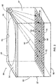
- FIG. 2 is a block diagram representation of one embodiment of the present invention.
- the optical sensor system 10 includes a first optical source 12 configured to transmit light in a defined path 14.
- the first optical source 12 may be any suitable source emitting radiation, for example, in the visible or infrared spectrums.
- the first optical source 12 may be, but is not limited to, a light emitting diode, an infrared diode, or a laser diode.
- the first optical source 12 may include one or more light sources and, optionally, may include a lens, a filter, or other optical device to direct, focus, or filter, the light being emitted from the source 12.
- the defined path 14 is, for example, a beam or a plane of light, which is intended to be transmitted to an optical sensor 50 either directly or by reflection, for example, from an object intersecting the defined path 14.
- the first optical source 12 may emit a plane of light along a defined path 14.
- multiple beams of light may be directed along the path 14.
- the path 14 intersects a conveyor, C, and is used to detect the presence, or absence, of an object along the conveyor, C.
- the conveyor, C may carry a pallet, P, of boxes, B, between two points.
- the light emitted from the first optical source 12 reflects off the boxes, B, and is detected by the optical sensor 50.
- the optical sensor 50 converts the light received at the sensor to an electrical signal 16 which is transmitted to a controller 30.
- the optical sensor 50 is capable of detecting light reflected off objects within its field of view 20.
- the electrical signal 16 generated by the sensor may be a binary on/off signal indicating the presence or absence of an object within the field of view 20 or, optionally, the electrical signal 16 may be an analog value corresponding to the intensity of light received by the optical sensor 50.
- the controller 30 uses the electrical signal 16 according to the application requirements, for example, to stop the conveyor, C, if an unexpected object is detected within the predefined path 14 or to reconstruct an image of the boxes, B, and pallet, P, passing through the predefined path 14. According to still another embodiment of the invention, at least a portion of the controller 30 may be incorporated into the optical sensor 50 to directly process the electrical signal 16. In addition, the controller 30 may provide a control signal 18 to the first optical source 12 to control the light emitted.
- the first optical source 12 and the optical sensor 50 may be configured to transmit and receive an optical beam in a defined path 14 configured to cross the path of the conveyor, C, either horizontally or at an angle and displaced above the conveyor, C.
- the optical sensor 50 may be configured to normally set the electrical signal 16 indicating it is receiving a beam of light from the optical source 12.
- the electrical signal 16 is reset if an object intersects the defined path 14.
- the first optical source 12 may be a single beam or multiple beams of light, defining, for example, a light curtain.
- the light curtain may be arranged horizontally and parallel with the conveyor to detect, for example, an operator reaching across the conveyor or into a protected region.
- the electrical signal 16 may be used by the controller 30 to disable the conveyor, C, or other mechanical device operating within the protected region upon detection of an object entering the protected region.
- the optical sensor 50 includes a housing 52 having a front wall 54 and a rear wall 56.
- the front wall 54 has an interior surface 53, an exterior surface 55, and an opening 58 that extends through the front wall 54 and is configured to allow incident light to pass into the optical sensor 50.
- a second optical source 60 is mounted on the interior surface 53 of the front wall 54.
- the second optical source 60 may be mounted on a side wall 57 or external to the optical sensor 50.
- the second optical source 60 may be, but is not limited to, a light emitting diode, an infrared diode, or a laser diode.
- An optical receiver 70 is mounted within the housing and configured to receive light incident to the sensor 50.
- the optical receiver 70 may be mounted, for example, to a substrate 72 proximate to the rear wall 56.
- the illustrated embodiment is intended to be exemplary and it is further contemplated that the optical sensor 50 may be of numerous shapes and configurations having for example no front wall or the optical receiver 70 positioned proximate to the front wall 54 of the sensor 50.
- the optical receiver 70 includes at least one photosensitive device 80.
- the photosensitive device 80 may be, for example, an active pixel sensor (APS), such as a complementary metal-oxide semiconductor (CMOS) sensor, or a passive pixel sensor (PPS) such as a charge coupled device (CCD).
- APS active pixel sensor
- PPS passive pixel sensor
- CCD charge coupled device
- the optical receiver 70 may include a single photosensitive device 80 to generate, for example, a binary signal, or an array of photosensitive pixels 80 to reproduce, for example, an image of an object.
- the optical receiver 70 may require control signals to select a row or column of signals 16 to be read from the array of pixels 80. It is further contemplated that a portion or all of the control functions from the controller 30 may be integrated with the receiver 70 onto an application specific integrated circuit (ASIC).
- ASIC application specific integrated circuit
- the second optical source 60 is used to test operation of the optical receiver 70.
- the controller 30 generates a control signal to enable the second optical source 60.
- the second optical source 60 is selected to emit radiation 62 at a sufficient intensity to saturate the photosensitive devices 80.
- the second optical source 60 is mounted such that the radiation 62 emitted by the source 60 saturates the entire optical receiver 70 whether the receiver 70 includes a single photosensitive device 80 or an array of photosensitive pixels 80. Because each photosensitive device 80 typically outputs a voltage as a function of the intensity of light received by the device 80, the resulting output voltage generated by each device 80 should be a known maximum value if the second optical source 60 is emitting radiation 62 sufficient to saturate the devices 80.
- the controller 30 identifies that photosensitive device 80 as underperforming. If one of the photosensitive devices 80 is generating no output voltage, the controller 30 identifies that photosensitive device 80 as failed.
- the photosensitive device 80 may generate a binary on/off signal responsive to the intensity of incident light received by the device 80 being greater than or less than a threshold level. If the photosensitive device 80 generates a binary on/off signal and remains off during the test, the controller 30 identifies that photosensitive device 80 as failed.
- An indicator signal is generated responsive to the test to indicate the status of the optical receiver 70 to an operator. If the receiver includes a single photosensitive device 80, determination that the device 80 is either underperforming or failed may be a critical fault condition and the indicator signal may be used to halt operation of equipment within a monitored region or to provide an operator with a visual or audio indication of the fault condition. If the optical receiver 70 includes an array of photosensitive devices 80, a threshold or maximum number of photosensitive devices 80 that may be identified as underperforming or failed may be selected. If the number of photosensitive devices 80 identified as underperforming or failed is within the acceptable range, the indicator signal may be set to indicate that the optical receiver 70 is operating normally. If the number of photosensitive devices 80 identified as underperforming or failed is outside the acceptable range, the indicator signal may be reset to indicate that the optical receiver 70 is no longer operating normally.
- the sensor system 10 may be used, for example, to detect unauthorized entry of a person or object into a restricted area or to detect the presence of a work-piece or part being transferred into a work zone.
- the optical source 12 may be one or more light beams establishing a light curtain, and each of the beams is received by one or more optical sensor units 50.
- the optical source 12 may generate a plane of light and the optical sensor unit 50 may be a 3-D camera that generates images of the objects from which the light is reflected.
- the type of optical source 12 and sensor unit 50 is selected according to the application requirements.
- testing of the optical sensor system 10 is coordinated with the normal monitoring function of the system 10.
- a command signal 18 from the controller 30 controls operation of the first optical source 12 which may be continuously enabled any time a particular zone is to be monitored.
- the first optical source 12 may be toggled on and off in coordination with the second optical source 60 mounted within the housing 52 of the optical sensor 50.
- Another command signal from the controller 30 similarly controls operation of the second optical source 60.
- the second optical source 60 is enabled during testing of the optical sensor 50. Because the second optical source 60 is configured to saturate the optical receiver 70, the first optical source 12 does not need to be disabled during the test.
- the test may be interleaved with the monitoring function.
- the safety requirements of an application typically provide a rate, or cycle time, at which the optical sensor 50 must be sampled to determine the intensity of light received from the first optical source 12 and, thereby, detecting the presence or absence of an object within the protected region.
- the optical sensor 50 must sample the light from the first optical source 12 and conduct any necessary diagnostics or performance checks according to the application requirements. Therefore, during this cycle, the controller 30 provides the control signal 18 to energize the first optical source 12, allows sufficient time for the optical sensor 50 to receive the radiated light, and reads the corresponding signal 16 from the optical sensor 50.
- the controller 30 may then de-energize the first optical source 12, if needed, and energize the second optical source 60. After sufficient time has passed for the photosensitive devices 80 to saturate, the controller 30 reads each of the signals from the photosensitive devices 80. After reading the signals from each of the photosensitive devices 80, the controller de-energizes the second optical source 60. The controller 30 may then determine whether any of the photosensitive devices 80 are under performing or have failed. Thus, the normal monitoring function and each of the test functions are each performed within the cycle time of the optical sensor 50.
Landscapes
- Engineering & Computer Science (AREA)
- Multimedia (AREA)
- Signal Processing (AREA)
- Health & Medical Sciences (AREA)
- Biomedical Technology (AREA)
- General Health & Medical Sciences (AREA)
- Geophysics And Detection Of Objects (AREA)
- Photometry And Measurement Of Optical Pulse Characteristics (AREA)
- Testing Of Individual Semiconductor Devices (AREA)
- Testing Of Optical Devices Or Fibers (AREA)
Claims (9)
- Capteur optique destiné à être utilisé dans un système de sécurité, comprenant
un boîtier (52) ;
un récepteur optique (70) monté dans le boîtier, dans lequel le récepteur optique comprend un réseau d'éléments photosensibles (80) qui génèrent chacun un signal correspondant à l'intensité de la lumière incidente sur l'élément photosensible ;
une source optique (60) montée dans le boîtier et configurée pour émettre une radiation à une intensité suffisante pour saturer le récepteur optique ; et
un circuit logique configuré pour :recevoir au moins un signal provenant du récepteur optique correspondant à l'intensité de la radiation reçue par le récepteur optique,comparer l'intensité de la radiation reçue par le récepteur optique à un seuil prédéterminé, etgénérer un signal indicateur en réponse à l'intensité de la radiation reçue par le récepteur optique,dans lequel :un seuil ou nombre maximum de dispositifs photosensibles est sélectionné, qui peut être identifié comme étant sous-performant ou défectueux ;si le nombre de dispositifs photosensibles identifiés comme étant sous-performants ou défectueux est compris dans une plage acceptable, le signal indicateur est réglé pour indiquer que le récepteur optique fonctionne normalement, etsi le nombre de dispositifs photosensibles identifiés comme étant sous-performants ou défectueux sort d'une plage acceptable, le signal indicateur est rétabli pour indiquer que le récepteur optique ne fonctionne plus normalement. - Capteur optique selon la revendication 1, dans lequel le récepteur optique comprend un dispositif photosensible qui génère un signal en réponse à l'intensité de la lumière incidente.
- Capteur optique selon la revendication 1, dans lequel le circuit logique reçoit les signaux provenant de chacun des éléments photosensibles et génère un signal indicateur pour chacun des éléments photosensibles qui ne sont pas réceptifs ou sont sous-performants.
- Capteur optique selon la revendication 1, dans lequel :le boîtier comprend :une paroi avant ayant une surface intérieure et une surface extérieure,une paroi arrière généralement opposée à la paroi avant, etune ouverture qui s'étend à travers la paroi avant ;le récepteur optique est monté sur un substrat situé à proximité de la paroi arrière et opposé à l'ouverture dans la paroi avant ; etla source optique est montée à proximité de la paroi avant.
- Capteur optique selon la revendication 1, dans lequel la source optique est sélectionnée parmi une diode électroluminescente, une diode infrarouge et une diode laser.
- Capteur optique selon la revendication 1, dans lequel le circuit logique est en outre configuré pour contrôler la source optique pour émettre la radiation et pour ensuite comparer l'intensité de la radiation reçue par le récepteur optique au seuil prédéterminé durant un premier intervalle périodique.
- Capteur optique selon la revendication 6, dans lequel le circuit logique est en outre configuré pour lire les signaux provenant du récepteur optique correspondant à l'intensité de la radiation reçue de la lumière incidente durant un deuxième intervalle périodique intercalé dans le premier intervalle périodique.
- Procédé de vérification du fonctionnement d'un capteur optique utilisé dans un système de sécurité, le capteur optique comportant un récepteur optique (70) monté dans un boîtier (52), dans lequel le récepteur optique comprend un réseau d'éléments photosensibles (80) qui génèrent chacun un signal correspondant à l'intensité de la lumière incidente sur l'élément photosensible, le procédé comprenant les étapes suivantes :montage d'une source optique (60) dans le boîtier, dans lequel la source optique émet une radiation à une intensité suffisante pour saturer le récepteur optique ;émission de la radiation par la source optique à un premier intervalle périodique ;génération d'un signal par le récepteur optique, qui correspond à l'intensité de la radiation détectée ;comparaison de l'intensité de la radiation détectée à un seuil prédéterminé ; etgénération d'un signal indicateur en réponse à la comparaison de l'intensité de la radiation au seuil prédéterminé,dans lequel :un seuil ou nombre maximum de dispositifs photosensibles est sélectionné, qui peut être identifié comme étant sous-performant ou défectueux ;si le nombre de dispositifs photosensibles identifiés comme étant sous-performants ou défectueux est compris dans une plage acceptable, le signal indicateur est réglé pour indiquer que le récepteur optique fonctionne normalement, etsi le nombre de dispositifs photosensibles identifiés comme étant sous-performants ou défectueux sort d'une plage acceptable, le signal indicateur est réinitialisé pour indiquer que le récepteur optique ne fonctionne plus normalement.
- Procédé selon la revendication 8, dans lequel les étapes suivantes sont mises en œuvre pour chacun des éléments photosensibles : génération du signal par le récepteur optique correspondant à l'intensité de la radiation détectée, comparaison de l'intensité de la radiation détectée au seuil prédéterminé, et génération du signal indicateur en réponse à la comparaison de l'intensité de la radiation au seuil prédéterminé.
Applications Claiming Priority (1)
| Application Number | Priority Date | Filing Date | Title |
|---|---|---|---|
| US13/401,329 US9083946B2 (en) | 2012-02-21 | 2012-02-21 | System to detect failed pixels in a sensor array |
Publications (3)
| Publication Number | Publication Date |
|---|---|
| EP2632167A2 EP2632167A2 (fr) | 2013-08-28 |
| EP2632167A3 EP2632167A3 (fr) | 2017-05-24 |
| EP2632167B1 true EP2632167B1 (fr) | 2020-10-14 |
Family
ID=47912900
Family Applications (1)
| Application Number | Title | Priority Date | Filing Date |
|---|---|---|---|
| EP13156168.0A Active EP2632167B1 (fr) | 2012-02-21 | 2013-02-21 | Système permettant de détecter des pixels défectueux dans un réseau de capteurs |
Country Status (3)
| Country | Link |
|---|---|
| US (1) | US9083946B2 (fr) |
| EP (1) | EP2632167B1 (fr) |
| CN (1) | CN103257368B (fr) |
Families Citing this family (6)
| Publication number | Priority date | Publication date | Assignee | Title |
|---|---|---|---|---|
| MX2021014474A (es) * | 2015-09-24 | 2022-10-31 | Hunt Perovskite Tech L L C | Sistema y metodo para probar degradacion de dispositivo fotosensible. |
| CN107688207A (zh) * | 2017-09-28 | 2018-02-13 | 重庆集元科技有限公司 | 测井放射源的全面监控方法 |
| DE102019102466A1 (de) * | 2019-01-31 | 2020-08-06 | Endress+Hauser Conducta Gmbh+Co. Kg | Optischer Sensor |
| DE102019114537A1 (de) * | 2019-05-29 | 2020-12-03 | OSRAM Opto Semiconductors Gesellschaft mit beschränkter Haftung | Optoelektronisches sensorbauelement zur lichtmessung mit eingebauter redundanz |
| CN114577336A (zh) * | 2022-02-25 | 2022-06-03 | 中国科学院合肥物质科学研究院 | 一种光电探测器阵列的标定方法及其系统 |
| CN114967832A (zh) * | 2022-05-23 | 2022-08-30 | 南昌航空大学 | 一种通过感光元件阵列输出控制信号的操纵器 |
Family Cites Families (13)
| Publication number | Priority date | Publication date | Assignee | Title |
|---|---|---|---|---|
| GB2303988A (en) * | 1995-07-31 | 1997-03-05 | Secr Defence | Thermal imaging system with detector array calibration mode |
| TR199801972T2 (xx) * | 1996-04-01 | 1999-01-18 | Lockheed Martin Corporation | Birle�ik halde laser/FLIR (ileri d�n�k enfraruj) optik sistem. |
| DE59804862D1 (de) * | 1997-09-15 | 2002-08-29 | Rms Kleine Gmbh Vertrieb Elekt | Verfahren und Vorrichtung zur optischen Überwachung eines Raumbereichs |
| US6285021B1 (en) * | 1999-07-27 | 2001-09-04 | Banner Engineering Corp. | Self checking safety switch |
| EP1269762B2 (fr) * | 2000-04-07 | 2018-04-11 | Pilz GmbH & Co. KG | Dispositif de securite servant a empecher l'acces a une zone dangereuse et procede pour verifier la securite de fonctionnement d'un tel dispositif |
| US6888572B1 (en) | 2000-10-26 | 2005-05-03 | Rockwell Science Center, Llc | Compact active pixel with low-noise image formation |
| US6655778B2 (en) * | 2001-10-02 | 2003-12-02 | Hewlett-Packard Development Company, L.P. | Calibrating system for a compact optical sensor |
| US7136157B2 (en) * | 2003-08-22 | 2006-11-14 | Micron Technology, Inc. | Method and apparatus for testing image sensors |
| US7081614B2 (en) | 2004-05-21 | 2006-07-25 | Raytheon Company | Optical sensor system with built-in optical test capability |
| DE102007008806C5 (de) * | 2006-10-27 | 2010-05-06 | Sick Ag | Optoelektronische Überwachung mit Test durch Dynamisierung |
| CN101210951B (zh) * | 2006-12-27 | 2010-12-22 | 中茂电子(深圳)有限公司 | 内建光源的光传感器检测装置及具该装置的测试机台 |
| TWI421482B (zh) * | 2008-12-02 | 2014-01-01 | Chi Lin Technology Co Ltd | 螢幕校正裝置與螢幕 |
| EP2199999B1 (fr) * | 2008-12-19 | 2012-05-02 | Pepperl + Fuchs GmbH | Procédé de test d'un capteur optique et capteur optique pouvant être testé |
-
2012
- 2012-02-21 US US13/401,329 patent/US9083946B2/en active Active
-
2013
- 2013-02-21 EP EP13156168.0A patent/EP2632167B1/fr active Active
- 2013-02-21 CN CN201310055501.5A patent/CN103257368B/zh not_active Expired - Fee Related
Non-Patent Citations (1)
| Title |
|---|
| None * |
Also Published As
| Publication number | Publication date |
|---|---|
| CN103257368A (zh) | 2013-08-21 |
| US20130215418A1 (en) | 2013-08-22 |
| EP2632167A2 (fr) | 2013-08-28 |
| US9083946B2 (en) | 2015-07-14 |
| EP2632167A3 (fr) | 2017-05-24 |
| CN103257368B (zh) | 2016-03-23 |
Similar Documents
| Publication | Publication Date | Title |
|---|---|---|
| US8872113B2 (en) | System to test performance of pixels in a sensor array | |
| US8094036B2 (en) | Monitoring device for a laser machining device | |
| US9083946B2 (en) | System to detect failed pixels in a sensor array | |
| US10132929B2 (en) | Light scanner | |
| US10113694B2 (en) | Time-of-flight safety photoelectric barrier and method of monitoring a protective field | |
| US8400314B2 (en) | Fire alarm | |
| US11624823B2 (en) | Safety laser scanner and method for maintaining operability | |
| KR102550578B1 (ko) | 안전 레이저 스캐너 및 전방 스크린 모니터링을 위한 방법 | |
| US11592552B2 (en) | Sensor and method for detecting an object | |
| KR101837806B1 (ko) | 다 광축 광전 센서 시스템 | |
| US20060043077A1 (en) | CO2 laser machining head with integrated monitoring device | |
| CN110132227B (zh) | 三角测量光传感器 | |
| US9768212B2 (en) | Method and apparatus for enabling sensors in a dual matrix sensor array | |
| US7671322B2 (en) | Optoelectronic security system for object detection in a monitored zone | |
| KR102373861B1 (ko) | Ccd 라인 센서를 이용한 비접촉식 구조물 변위 측정 시스템 | |
| CN114859318A (zh) | 具有射束光学诊断的激光雷达系统 | |
| JP2022534574A (ja) | ビルトイン式冗長性を備えた光測定のためのオプトエレクトロニクスセンサコンポーネント | |
| JP7581988B2 (ja) | アーク故障検出装置 | |
| CN107003180A (zh) | 用于监测辐射的方法 | |
| KR20100127431A (ko) | 레이저 비전 시스템 | |
| HK1099162B (en) | Device for monitoring a spatial area, especially for securing a hazardous area of an automated installation |
Legal Events
| Date | Code | Title | Description |
|---|---|---|---|
| PUAI | Public reference made under article 153(3) epc to a published international application that has entered the european phase |
Free format text: ORIGINAL CODE: 0009012 |
|
| AK | Designated contracting states |
Kind code of ref document: A2 Designated state(s): AL AT BE BG CH CY CZ DE DK EE ES FI FR GB GR HR HU IE IS IT LI LT LU LV MC MK MT NL NO PL PT RO RS SE SI SK SM TR |
|
| AX | Request for extension of the european patent |
Extension state: BA ME |
|
| PUAL | Search report despatched |
Free format text: ORIGINAL CODE: 0009013 |
|
| AK | Designated contracting states |
Kind code of ref document: A3 Designated state(s): AL AT BE BG CH CY CZ DE DK EE ES FI FR GB GR HR HU IE IS IT LI LT LU LV MC MK MT NL NO PL PT RO RS SE SI SK SM TR |
|
| AX | Request for extension of the european patent |
Extension state: BA ME |
|
| RIC1 | Information provided on ipc code assigned before grant |
Ipc: H04N 5/225 20060101ALI20170418BHEP Ipc: H04N 5/367 20110101ALN20170418BHEP Ipc: H04N 17/00 20060101AFI20170418BHEP |
|
| STAA | Information on the status of an ep patent application or granted ep patent |
Free format text: STATUS: REQUEST FOR EXAMINATION WAS MADE |
|
| 17P | Request for examination filed |
Effective date: 20171113 |
|
| RBV | Designated contracting states (corrected) |
Designated state(s): AL AT BE BG CH CY CZ DE DK EE ES FI FR GB GR HR HU IE IS IT LI LT LU LV MC MK MT NL NO PL PT RO RS SE SI SK SM TR |
|
| GRAP | Despatch of communication of intention to grant a patent |
Free format text: ORIGINAL CODE: EPIDOSNIGR1 |
|
| STAA | Information on the status of an ep patent application or granted ep patent |
Free format text: STATUS: GRANT OF PATENT IS INTENDED |
|
| RIC1 | Information provided on ipc code assigned before grant |
Ipc: H04N 5/225 20060101ALI20200429BHEP Ipc: H04N 17/00 20060101AFI20200429BHEP Ipc: H04N 5/367 20110101ALN20200429BHEP |
|
| RIC1 | Information provided on ipc code assigned before grant |
Ipc: H04N 5/225 20060101ALI20200507BHEP Ipc: H04N 17/00 20060101AFI20200507BHEP Ipc: H04N 5/367 20110101ALN20200507BHEP |
|
| INTG | Intention to grant announced |
Effective date: 20200603 |
|
| GRAS | Grant fee paid |
Free format text: ORIGINAL CODE: EPIDOSNIGR3 |
|
| GRAA | (expected) grant |
Free format text: ORIGINAL CODE: 0009210 |
|
| STAA | Information on the status of an ep patent application or granted ep patent |
Free format text: STATUS: THE PATENT HAS BEEN GRANTED |
|
| AK | Designated contracting states |
Kind code of ref document: B1 Designated state(s): AL AT BE BG CH CY CZ DE DK EE ES FI FR GB GR HR HU IE IS IT LI LT LU LV MC MK MT NL NO PL PT RO RS SE SI SK SM TR |
|
| REG | Reference to a national code |
Ref country code: GB Ref legal event code: FG4D |
|
| REG | Reference to a national code |
Ref country code: AT Ref legal event code: REF Ref document number: 1324716 Country of ref document: AT Kind code of ref document: T Effective date: 20201015 Ref country code: CH Ref legal event code: EP |
|
| REG | Reference to a national code |
Ref country code: DE Ref legal event code: R096 Ref document number: 602013073227 Country of ref document: DE |
|
| REG | Reference to a national code |
Ref country code: IE Ref legal event code: FG4D |
|
| REG | Reference to a national code |
Ref country code: AT Ref legal event code: MK05 Ref document number: 1324716 Country of ref document: AT Kind code of ref document: T Effective date: 20201014 |
|
| REG | Reference to a national code |
Ref country code: NL Ref legal event code: MP Effective date: 20201014 |
|
| PG25 | Lapsed in a contracting state [announced via postgrant information from national office to epo] |
Ref country code: FI Free format text: LAPSE BECAUSE OF FAILURE TO SUBMIT A TRANSLATION OF THE DESCRIPTION OR TO PAY THE FEE WITHIN THE PRESCRIBED TIME-LIMIT Effective date: 20201014 Ref country code: RS Free format text: LAPSE BECAUSE OF FAILURE TO SUBMIT A TRANSLATION OF THE DESCRIPTION OR TO PAY THE FEE WITHIN THE PRESCRIBED TIME-LIMIT Effective date: 20201014 Ref country code: NO Free format text: LAPSE BECAUSE OF FAILURE TO SUBMIT A TRANSLATION OF THE DESCRIPTION OR TO PAY THE FEE WITHIN THE PRESCRIBED TIME-LIMIT Effective date: 20210114 Ref country code: PT Free format text: LAPSE BECAUSE OF FAILURE TO SUBMIT A TRANSLATION OF THE DESCRIPTION OR TO PAY THE FEE WITHIN THE PRESCRIBED TIME-LIMIT Effective date: 20210215 Ref country code: NL Free format text: LAPSE BECAUSE OF FAILURE TO SUBMIT A TRANSLATION OF THE DESCRIPTION OR TO PAY THE FEE WITHIN THE PRESCRIBED TIME-LIMIT Effective date: 20201014 Ref country code: GR Free format text: LAPSE BECAUSE OF FAILURE TO SUBMIT A TRANSLATION OF THE DESCRIPTION OR TO PAY THE FEE WITHIN THE PRESCRIBED TIME-LIMIT Effective date: 20210115 |
|
| REG | Reference to a national code |
Ref country code: LT Ref legal event code: MG4D |
|
| PG25 | Lapsed in a contracting state [announced via postgrant information from national office to epo] |
Ref country code: ES Free format text: LAPSE BECAUSE OF FAILURE TO SUBMIT A TRANSLATION OF THE DESCRIPTION OR TO PAY THE FEE WITHIN THE PRESCRIBED TIME-LIMIT Effective date: 20201014 Ref country code: AT Free format text: LAPSE BECAUSE OF FAILURE TO SUBMIT A TRANSLATION OF THE DESCRIPTION OR TO PAY THE FEE WITHIN THE PRESCRIBED TIME-LIMIT Effective date: 20201014 Ref country code: BG Free format text: LAPSE BECAUSE OF FAILURE TO SUBMIT A TRANSLATION OF THE DESCRIPTION OR TO PAY THE FEE WITHIN THE PRESCRIBED TIME-LIMIT Effective date: 20210114 Ref country code: PL Free format text: LAPSE BECAUSE OF FAILURE TO SUBMIT A TRANSLATION OF THE DESCRIPTION OR TO PAY THE FEE WITHIN THE PRESCRIBED TIME-LIMIT Effective date: 20201014 Ref country code: SE Free format text: LAPSE BECAUSE OF FAILURE TO SUBMIT A TRANSLATION OF THE DESCRIPTION OR TO PAY THE FEE WITHIN THE PRESCRIBED TIME-LIMIT Effective date: 20201014 Ref country code: IS Free format text: LAPSE BECAUSE OF FAILURE TO SUBMIT A TRANSLATION OF THE DESCRIPTION OR TO PAY THE FEE WITHIN THE PRESCRIBED TIME-LIMIT Effective date: 20210214 Ref country code: LV Free format text: LAPSE BECAUSE OF FAILURE TO SUBMIT A TRANSLATION OF THE DESCRIPTION OR TO PAY THE FEE WITHIN THE PRESCRIBED TIME-LIMIT Effective date: 20201014 |
|
| PG25 | Lapsed in a contracting state [announced via postgrant information from national office to epo] |
Ref country code: HR Free format text: LAPSE BECAUSE OF FAILURE TO SUBMIT A TRANSLATION OF THE DESCRIPTION OR TO PAY THE FEE WITHIN THE PRESCRIBED TIME-LIMIT Effective date: 20201014 |
|
| REG | Reference to a national code |
Ref country code: DE Ref legal event code: R097 Ref document number: 602013073227 Country of ref document: DE |
|
| PG25 | Lapsed in a contracting state [announced via postgrant information from national office to epo] |
Ref country code: RO Free format text: LAPSE BECAUSE OF FAILURE TO SUBMIT A TRANSLATION OF THE DESCRIPTION OR TO PAY THE FEE WITHIN THE PRESCRIBED TIME-LIMIT Effective date: 20201014 Ref country code: SK Free format text: LAPSE BECAUSE OF FAILURE TO SUBMIT A TRANSLATION OF THE DESCRIPTION OR TO PAY THE FEE WITHIN THE PRESCRIBED TIME-LIMIT Effective date: 20201014 Ref country code: LT Free format text: LAPSE BECAUSE OF FAILURE TO SUBMIT A TRANSLATION OF THE DESCRIPTION OR TO PAY THE FEE WITHIN THE PRESCRIBED TIME-LIMIT Effective date: 20201014 Ref country code: SM Free format text: LAPSE BECAUSE OF FAILURE TO SUBMIT A TRANSLATION OF THE DESCRIPTION OR TO PAY THE FEE WITHIN THE PRESCRIBED TIME-LIMIT Effective date: 20201014 Ref country code: EE Free format text: LAPSE BECAUSE OF FAILURE TO SUBMIT A TRANSLATION OF THE DESCRIPTION OR TO PAY THE FEE WITHIN THE PRESCRIBED TIME-LIMIT Effective date: 20201014 Ref country code: CZ Free format text: LAPSE BECAUSE OF FAILURE TO SUBMIT A TRANSLATION OF THE DESCRIPTION OR TO PAY THE FEE WITHIN THE PRESCRIBED TIME-LIMIT Effective date: 20201014 |
|
| PLBE | No opposition filed within time limit |
Free format text: ORIGINAL CODE: 0009261 |
|
| STAA | Information on the status of an ep patent application or granted ep patent |
Free format text: STATUS: NO OPPOSITION FILED WITHIN TIME LIMIT |
|
| PG25 | Lapsed in a contracting state [announced via postgrant information from national office to epo] |
Ref country code: DK Free format text: LAPSE BECAUSE OF FAILURE TO SUBMIT A TRANSLATION OF THE DESCRIPTION OR TO PAY THE FEE WITHIN THE PRESCRIBED TIME-LIMIT Effective date: 20201014 |
|
| 26N | No opposition filed |
Effective date: 20210715 |
|
| PG25 | Lapsed in a contracting state [announced via postgrant information from national office to epo] |
Ref country code: MC Free format text: LAPSE BECAUSE OF FAILURE TO SUBMIT A TRANSLATION OF THE DESCRIPTION OR TO PAY THE FEE WITHIN THE PRESCRIBED TIME-LIMIT Effective date: 20201014 |
|
| REG | Reference to a national code |
Ref country code: BE Ref legal event code: MM Effective date: 20210228 |
|
| PG25 | Lapsed in a contracting state [announced via postgrant information from national office to epo] |
Ref country code: LI Free format text: LAPSE BECAUSE OF NON-PAYMENT OF DUE FEES Effective date: 20210228 Ref country code: LU Free format text: LAPSE BECAUSE OF NON-PAYMENT OF DUE FEES Effective date: 20210221 Ref country code: IT Free format text: LAPSE BECAUSE OF FAILURE TO SUBMIT A TRANSLATION OF THE DESCRIPTION OR TO PAY THE FEE WITHIN THE PRESCRIBED TIME-LIMIT Effective date: 20201014 Ref country code: AL Free format text: LAPSE BECAUSE OF FAILURE TO SUBMIT A TRANSLATION OF THE DESCRIPTION OR TO PAY THE FEE WITHIN THE PRESCRIBED TIME-LIMIT Effective date: 20201014 Ref country code: CH Free format text: LAPSE BECAUSE OF NON-PAYMENT OF DUE FEES Effective date: 20210228 |
|
| PG25 | Lapsed in a contracting state [announced via postgrant information from national office to epo] |
Ref country code: SI Free format text: LAPSE BECAUSE OF FAILURE TO SUBMIT A TRANSLATION OF THE DESCRIPTION OR TO PAY THE FEE WITHIN THE PRESCRIBED TIME-LIMIT Effective date: 20201014 |
|
| PG25 | Lapsed in a contracting state [announced via postgrant information from national office to epo] |
Ref country code: IE Free format text: LAPSE BECAUSE OF NON-PAYMENT OF DUE FEES Effective date: 20210221 |
|
| PG25 | Lapsed in a contracting state [announced via postgrant information from national office to epo] |
Ref country code: IS Free format text: LAPSE BECAUSE OF FAILURE TO SUBMIT A TRANSLATION OF THE DESCRIPTION OR TO PAY THE FEE WITHIN THE PRESCRIBED TIME-LIMIT Effective date: 20210214 |
|
| PG25 | Lapsed in a contracting state [announced via postgrant information from national office to epo] |
Ref country code: BE Free format text: LAPSE BECAUSE OF NON-PAYMENT OF DUE FEES Effective date: 20210228 |
|
| PG25 | Lapsed in a contracting state [announced via postgrant information from national office to epo] |
Ref country code: HU Free format text: LAPSE BECAUSE OF FAILURE TO SUBMIT A TRANSLATION OF THE DESCRIPTION OR TO PAY THE FEE WITHIN THE PRESCRIBED TIME-LIMIT; INVALID AB INITIO Effective date: 20130221 |
|
| P01 | Opt-out of the competence of the unified patent court (upc) registered |
Effective date: 20230404 |
|
| PG25 | Lapsed in a contracting state [announced via postgrant information from national office to epo] |
Ref country code: CY Free format text: LAPSE BECAUSE OF FAILURE TO SUBMIT A TRANSLATION OF THE DESCRIPTION OR TO PAY THE FEE WITHIN THE PRESCRIBED TIME-LIMIT Effective date: 20201014 |
|
| PG25 | Lapsed in a contracting state [announced via postgrant information from national office to epo] |
Ref country code: MK Free format text: LAPSE BECAUSE OF FAILURE TO SUBMIT A TRANSLATION OF THE DESCRIPTION OR TO PAY THE FEE WITHIN THE PRESCRIBED TIME-LIMIT Effective date: 20201014 |
|
| PG25 | Lapsed in a contracting state [announced via postgrant information from national office to epo] |
Ref country code: TR Free format text: LAPSE BECAUSE OF FAILURE TO SUBMIT A TRANSLATION OF THE DESCRIPTION OR TO PAY THE FEE WITHIN THE PRESCRIBED TIME-LIMIT Effective date: 20201014 |
|
| PG25 | Lapsed in a contracting state [announced via postgrant information from national office to epo] |
Ref country code: MT Free format text: LAPSE BECAUSE OF FAILURE TO SUBMIT A TRANSLATION OF THE DESCRIPTION OR TO PAY THE FEE WITHIN THE PRESCRIBED TIME-LIMIT Effective date: 20201014 |
|
| PGFP | Annual fee paid to national office [announced via postgrant information from national office to epo] |
Ref country code: GB Payment date: 20260121 Year of fee payment: 14 |
|
| PGFP | Annual fee paid to national office [announced via postgrant information from national office to epo] |
Ref country code: DE Payment date: 20260121 Year of fee payment: 14 |
|
| PGFP | Annual fee paid to national office [announced via postgrant information from national office to epo] |
Ref country code: FR Payment date: 20260121 Year of fee payment: 14 |