EP2632626B1 - Jonction d'une première pièce structurale à une deuxième pièce structurale par soudage unilatéral par points par résistance - Google Patents
Jonction d'une première pièce structurale à une deuxième pièce structurale par soudage unilatéral par points par résistance Download PDFInfo
- Publication number
- EP2632626B1 EP2632626B1 EP11764686.9A EP11764686A EP2632626B1 EP 2632626 B1 EP2632626 B1 EP 2632626B1 EP 11764686 A EP11764686 A EP 11764686A EP 2632626 B1 EP2632626 B1 EP 2632626B1
- Authority
- EP
- European Patent Office
- Prior art keywords
- welding
- components
- component
- resistance spot
- resistance
- Prior art date
- Legal status (The legal status is an assumption and is not a legal conclusion. Google has not performed a legal analysis and makes no representation as to the accuracy of the status listed.)
- Active
Links
Images

Classifications
-
- B—PERFORMING OPERATIONS; TRANSPORTING
- B23—MACHINE TOOLS; METAL-WORKING NOT OTHERWISE PROVIDED FOR
- B23K—SOLDERING OR UNSOLDERING; WELDING; CLADDING OR PLATING BY SOLDERING OR WELDING; CUTTING BY APPLYING HEAT LOCALLY, e.g. FLAME CUTTING; WORKING BY LASER BEAM
- B23K11/00—Resistance welding; Severing by resistance heating
- B23K11/10—Spot welding; Stitch welding
- B23K11/11—Spot welding
Definitions
- the invention relates to a method for joining a first component to a second component by means of a one-sided resistance spot welding.
- Resistance spot welding is known. It can be joined together electrically conductive and fusible components.
- a welding electrode is pressed against one of the components on one side in an electrically conductive contact, wherein a welding current through the components can be built up from the welding electrode to a dummy electrode.
- WO 2004/087360 A1 is a one-sided resistance spot welding of sheets, in which a current path and an electrode force are concentrated in the region of a hump in a top plate, known.
- the DE 199 47 206 B4 relates to a method for connecting two components, in particular on a motor vehicle, by projection welding, in which a component has at least one raised weld boss which rests in a weld zone, preferably a spot weld zone, with a contact point on the other component, wherein the weld boss with a hump base having the abutment surface forming base surface, wherein in the base surface a raised humpback structure is embossed with a plurality of projection projections, wherein during passage of current through the welding zone of the weld hermetic melting of the humpback structure and on the other component a preferably thin enamel layer is formed, so that the two components After their compression in the weld zone form a component connection without surface damage.
- the DE 10 2009 023 792 A1 relates to a joining method for a stack of three metal sheets, which is carried out using only a single welding step, with access to only one side of the plate is required.
- An inner plate of the stack has a pair of forked humps formed therein, at least a first apex facing in one direction and at least a second apex facing in the opposite direction.
- First and second outer metal sheets are assembled to the inner panel with the first outer panel abutting the at least one first vertex and the second outer panel abutting the at least one second vertex.
- a projection welder welds the plates with the help of a Accessing only the first outer plate overlying the bifurcated bosses, with a majority of the current flowing through the second outer plate.
- a welding method that focuses on electrodes having spherically-formed end portions that cause deformation in a portion of the upper workpiece to be welded.
- a current flow between the electrodes is effected, wherein the deformed region is in contact with the second workpiece to be welded, so that the first and the second workpiece are welded together.
- a joining method is known in which a ground electrode is pressed in the same direction of action against a second workpiece, such as a joining electrode to a first workpiece.
- a method for joining folded flanges wherein a steel plate is arranged as a second component between an upper component and a lower component of a first component.
- the first component is a plywood laminated with steel, which contains a plastic resin layer, which is melted during joining.
- the steel plate has a concave shape in the area that lies between the folding components, wherein in the concave area a solid heat-insulating material is provided to protect the steel laminate from excessive heat.
- a welding electrode is pressed onto the upper component while a dummy electrode rests on the steel plate.
- the welding electrode is heated to approximately 300 ° C., wherein the layer is melted and a welding point is placed between the first and second component.
- the object of the invention is to enable an improved joining of a first component to a second component by means of one-sided resistance spot welding. in particular, to improve a concentration of a welding current in a range of a resistance point of the one-sided resistance spot welding.
- the object is achieved in a method for joining a first component to a second component by means of a one-sided resistance spot welding according to claim 1.
- a band of the spacer device is inserted between the components, the components being locally approximated to one another in the region of the respective resistance point during the resistance spot welding through the at least one recess and the respective resistance point surrounding the insulating effect of the insulating tape is maintained.
- the two components by means of the introduced insulating tape simultaneously spaced from each other and electrically isolated from each other.
- the two components can be approached in the region of the recess of the insulating tape by pressing the welding electrode to such an extent that they touch and thereby the welding current can flow.
- the spacer device has at least one projection of at least one of the components.
- one of the components may have the projection of the spacer device, wherein no separate spacer device must be positioned relative to the components.
- the spacer device can be attached directly to a manufacturing process of the corresponding component with this. It is possible, the spacer device integral with the component in question perform. Alternatively and / or additionally, the spacer device can be attached separately to the corresponding component, in particular during a production process. It is conceivable that the separately mounted spacer device has insulating properties.
- a further embodiment of the method not covered by the invention is carried out with the introduction of the insulating tape and at a distance therefrom, in particular spaced parallel, another insulating tape for producing the spacing, the resistance point lying between the insulating tapes.
- the components can be spaced next to the resistance point by means of the two insulating strips and arranged electrically isolated from each other.
- the actual welding process ie the approach of the components by the pressing of the welding electrode and the introduction of the welding current, can be done between the insulating tapes.
- a further embodiment of the method not covered by the invention is carried out by introducing an electrical preheating current into the components and thereby melting the insulating tape at least in the region of the resistance point.
- the liquefied insulating tape can be displaced during pressing of the welding electrode, so that touching the two components in the region of the resistance point, so that the welding current can flow to melt and join the components.
- a further embodiment of the method not covered by the invention is carried out by introducing the preheating current via a fixing point which electrically contacts the components.
- the preheating current can be conducted via the fixing point.
- the components can be prefixed by means of the fixing point in a position relative to each other.
- the preheating current can be passed over existing welding points, the preheating current for the first time over the fixing point and then flows over already made welds.
- a further embodiment of the method which is not encompassed by the invention is carried out by introducing a band which is electrically conductive at least in the region of the welding point for producing the distance, introducing the electric preheating current via the electrically conductive band and melting the electrically conductive band by means of the electric preheating current.
- an electrical resistance of the conductive tape can be adjusted so that this is due to the preheating heated comparatively strong and thereby melted. For a first-time production of a welding point, no fixing point for introducing the preheating current is necessary. Rather, this can be made directly on the electrically conductive tape.
- the electrically conductive strip which has been melted by means of the preheating current can be displaced in the region of the resistance point by the pressing-on of the welding electrode and the associated approach of the components, so that the welding current can flow.
- the approach of the components can be carried out under elastic deformation of one of the components due to the contact pressure of the welding electrode.
- the object is also achieved in a welding apparatus for one-sided resistance spot welding with a dummy electrode and a welding electrode, wherein the welding apparatus is designed to carry out the method described above. This results in the advantages described above.
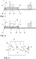
- FIG. 1 shows a schematic side view of a welding device 1 shown only partially.
- the welding device 1 has a welding electrode 3 and a dummy electrode 5. Between the welding electrode 3 and the dummy electrode 5, a voltage for inducing a preheating current and / or a welding current for joining a first component 7 and a second component 9 can be applied.
- the first component 7 may, for example, be a top plate and the second component 9 may be a bottom plate.
- the components 7 and 9 may be components, in particular body parts, of a motor vehicle.
- the components 7 and 9 are prepared for unilateral resistance spot welding by the welding apparatus 1.
- the welding electrode 3 and the dummy electrode 5 are attached from the same side to the components 7 and 9 or attachable or electrically contacted or contacted.
- the components 7 and 9 are arranged in the region of a resistance point 11 at a distance 13 from each other.
- the components 7 and 9 are in particular planar components, which in the in Fig. 1 shown prepared relative position to each other the distance 13 to each other.
- the components 7 and 9 may also be curved components which have the spacing 13, in particular in the region of the resistance point 11.
- the distance 13 is made by means of a spacer device 15.
- the spacer device 15 according to the embodiment not included in the invention according to the FIGS. 1 to 3 Projections 17 which are integrally connected to the first component 7.
- the projections 17 may be integrally connected to the second component 9, which is not included in the invention.
- the projections 17 of the spacer device 15 may be designed as separate components, which are arranged, for example, for preparing the resistance spot welding between the components 7 and 9 for producing the distance 13, which is not covered by the invention.
- Fig. 2 shows the in Fig. 1 shown welding device during a welding operation for performing the resistance spot welding.
- the welding electrode 3 is pressed with a contact force against the first component 7.
- the contact force and its direction is in Fig. 2 symbolized by an arrow 19.
- the first component 7 is elastically deformed so that it has a curvature.
- the distance 13 is reduced to a value of 0, so that the first component 7 and the second component 9 are in an electrically conductive contact with each other.
- a welding current (not shown) can flow from the welding electrode 3 via the first component 7, the second component 9 to the dummy electrode 5.
- the resistance point 11 of the components 7 and 9 is advantageously melted, so that forms a weld lens for joining the components 7 and 9.
- the welding current of the welding device 1 in the resistance point 11 can be concentrated so that the weld nugget can form on the first component 7 and the second component 9.
- a shunt forms, which causes a side stream.
- this is advantageous so small that thereby the actual welding process is not affected. If appropriate, a current flow generated by means of the welding device 1 can be increased by the electrical current flowing through the shunt.
- Fig. 3 shows a plan view of the two in the Fig. 1 and 2 shown components 7 and 9. It is the resistance point 11 can be seen in Fig. 3 symbolized by a circle.
- the resistance point 11 can also be referred to as a welding zone, in which forms the necessary to join the components 7 and 9 nugget.
- the first component 7 and the second component 9 overlap in an overlapping zone 21, which is symbolized by means of a double arrow and dashed lines in FIG.
- the overlapping zone 21 may, for example, be between 10 and 30 mm, in particular between 12 and 20 mm, in particular approximately 16 mm.
- the spacer device 15 has a total of four trapezoidally arranged, not included in the invention projections 17, which can also be referred to as a distance hump.
- the projections 17 not encompassed by the invention are arranged outside the resistance point 11, whereby only a secondary flow which is insufficient for welding flows over them.
- these only provide the distance 13 between the components 7 and 9, which advantageously remains outside the resistance point 11, so that advantageously only via the projections 17 of the spacer device 15 and the resistance point 11 itself, an electric current flow takes place.
- the welding current required for welding the components 7 and 9 can advantageously be concentrated in the resistance point 11 of the components 7 and 9.
- the Fig. 4-7 each show a schematic plan view of two spaced-apart components 7 and 9, which are available by means of the welding device 1, analogous to the representation of Fig. 3 , In contrast, have the components 7 and 9 as shown in the Fig. 4-6 in each case a plurality of resistance points 11 and are each separated by a band 23 from each other. It shows Fig. 4 the embodiment encompassed by the invention.
- Fig. 4 it is a tape 23 with insulating properties, so an insulating tape.
- This in Fig. 4 illustrated band 23 is disposed between the components 7 and 9 and has 11 recesses 25 in the region of the resistance points.
- the recesses 25 are shown in the representation of Fig. 4 executed as an example round. However, the recesses 25 may also have a different geometric shape, for example square and / or the like.
- the components 7 and 9 during the resistance spot welding through the recesses 25 can be locally approximated to each other in the region of the respective resistance point 11, wherein advantageously the respective resistance point 11 surrounding the insulating effect of the belt 23 is maintained.
- Fig. 5 shows a further, not embraced by the invention embodiment, wherein the band 23 is made narrower, so that this covers, for example, approximately only 1/3 of the overlapping zone 21.
- another band 27 is arranged.
- the bands 23 and 27 are arranged parallel to one another and at a distance from one another in the region of the overlapping zone 21.
- the components 7 and 9 are arranged spaced from each other before performing the resistance point welding, leaving in the space of the distance 13 a surmountable air space by pressing the welding electrode 3 to a distance of 0th can be reduced so that the components 7 and 9 touch each other at the respective resistance point 11 for making the electrical contact.
- the electrically insulating effect of the bands 23 and 27 and an electrical insulation due to the remaining air space remains surrounding the resistance point 11 obtained, so that advantageously the welding current of the resistance spot welding in the respective resistance point 11 is concentrated.
- Fig. 6 shows a further, not included in the invention embodiment of the welding device 1, wherein in contrast the band 23 has no recesses 25.
- the tape 23 has, according to the not covered by the invention representation of Fig. 6 thermoplastic properties and can be melted by heating.
- the components 7 and 9 are electrically contacted with each other by means of an electrically conductive fixing point 29.
- a preheating current for melting the band 23 in the region of the resistance point 11 into the components 7 and 9 can be introduced.
- the molten strip 23 is displaced locally, so that an electrically conductive contact between the components 7 and 9 can be produced in the region of the resistance point 11.
- the molten strip 23 also has electrically insulating properties in the liquid state, so that advantageously the electric welding current in the region of the resistance point 11 can be concentrated.
- the band 23 is not provided, or ends adjacent thereto.
- a belt 23 with electrically conductive properties is arranged between the components 7 and 9, a belt 23 with electrically conductive properties.
- the electrically conductive belt 23 according to the representation 7 not encompassed by the invention has no recesses, that is, it is arranged continuously in the overlapping zone 21 between the components 7 and 9 for producing the spacing 13.
- the band 23 has insulating properties and is also arranged, with the exception of the fixing point 29, continuously in the overlapping zone 21 between the components 7 and 9, is not according to the invention included illustration of Fig. 7 no fixing point 29 required.
- the preheating current can be conducted via the strip 23 having electrically conductive properties itself.
- the electrically conductive tape 23 may also have thermoplastic properties and is meltable. The electrically conductive properties can be adjusted so that a safe heating of the belt 23 according to the Fig. 7 when passing the preheating current results. Analogously to the procedure described above, the electrically conductive strip can also be melted so that it can be displaced locally during the pressing of the welding electrode 3 in the region of the resistance point 11 for producing the electrical contact contact between the components 7 and 9.
- the presentation of the Fig. 9 shows in principle the displacement of the molten strip 23 analogous to that encompassed by the invention 6 and 7 , Analogously, but without the need for liquefaction by a preheating current, if necessary, it is the case with the band 23 with recess 25 of the embodiment encompassed by the invention Fig. 4 or the spaced bands 23 and 27 according to the not included in the invention representation in FIG Fig. 5 , wherein in each case also in the region of the resistance point 11, the components 7 and 9 are approximated in an electrical contact with each other.
- Fig. 8 shows the schematic side view of the welding device 1 of Fig. 9 , In Fig. 8 It can be seen that between the components 7 and 9, the belt 23 is arranged for producing the distance 13. According to the representations of the Fig. 4-6 the tape 23 is an insulating layer, wherein only the embodiment of Fig. 4 is encompassed by the invention. According to the not covered by the invention representation of the Fig. 7 The band 23 has electrically conductive properties and can convert a preheating current directly into a reflow.
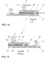
- Fig. 10 shows a schematic view of two components 7 and 9 together with a welding electrode 3 and a dummy electrode 5. Between the components 7 and 9, a band 23 is arranged with insulating properties.
- a band 23 is arranged with insulating properties.
- the invention fixing point 29 or an already welded resistance point 11 In the presentation of the Fig. 10 to the right of the welding electrode 3 and the dummy electrode 5 is a non-embraced by the invention fixing point 29 or an already welded resistance point 11. It can be seen that a preheating of the welding electrode 3 via the not covered by the invention fixing point 29 or the already welded resistance point 11 flows through the first component 7 and the second component 9 to the dummy electrode 5. In this case, the band 23 is heated and melted.
- Fig. 11 shows the in Fig. 10 shown sectional view of the components 7 and 9 together with the welding electrode 3 and the dummy electrode 5.
- Fig. 11 already reduces the distance 13 by pressing the welding electrode 3 to 0, so that the components 7 and 9 are in the region of the resistance point 11 in an electrically conductive contact.
- a total current 35 conducted via the welding electrode 3 and the dummy electrode 5 is divided into a secondary flow 37 and a welding flow 33.
- the secondary current 37 flows over the resistance point 11 already produced.
- the welding current 33 which is substantially greater, flows over the resistance point 11 located below the welding electrode 3 and leads to the melting of the first component 7 and of the second component 9.
- the total current 35 flows as a preheating current 31 via the fixing point 29 not covered by the invention or the resistance point 11 already produced, ie it represents the preheating current 31 or is identical to these.
- the distance hump not included in the invention of the spacer 15 are provided.
- a band 23 is provided in order to arrange the components 7 and 9 at a distance 13 from one another, as shown in FIG Fig. 4 is shown.
- the spacer device 15 has the in the Fig. 5-7 shown band 23 and the further band 27 on.
- the welding current 33 can be concentrated in the resistance point 11 in such a way that more advantageous process windows or larger process windows result and / or certain material combinations of the components 7 and 9 can be added by resistance spot welding.
- current paths of the welding current 33 are constricted to the region of the resistance point 11.
- the protrusions 17 or spacer bosses of the spacer device 15 not encompassed by the invention can be embossed into the first component 7, so that an insulating air gap of the spacing 13 between the components 7 and 9, in particular sheets, can be produced.
- the electrodes 3 and 5 are advantageously positioned at a suitable location, at the resistance point 11, which lies between the projections 17 of the spacer device 15 not covered by the invention.
- the electrode force of the welding electrode 3 shown by means of the arrow 19 deforms the first component 7, this region being pressed in an electrically conductive manner onto the second component 9, whereby the circuit for inducing the welding current 33 is closed.
- a shunt current across the not covered by the invention projections 17 of Distance device 15 are compensated, but this is so small compared to a direct contact contact of the components 7 and 9, that in the region of the resistance point 11, the joining of the components 7 and 9 can be done in a safe and simple manner.
- the projections 17 of the spacer device 15, which are not covered by the invention, can be designed as pointed round bumps, resulting in a high contact resistance, wherein the secondary flow 37 or shunt current can be kept low.
- the spacer device 15 with the projections 17 not covered by the invention advantageously serves only for producing the distance 13, that is to say has no function with regard to heat conduction during resistance spot welding. As in the Fig.
- the number of projections 17 of the spacer device 15 not encompassed by the invention can optionally be varied, for example, a trapezoidal arrangement of a total of 4 distance humps and a width of 16 mm of the overlapping zone 21 can be selected.
- the welding device 1 may have a welding control for regulating the welding current 33.
- the tape 23 as shown in the Fig. 4 is designed as an adhesive tape, which can be glued in a preparatory step in a simple manner on one of the components 7 and 9.
- the tape 23 has adhesively adhesive properties so that it builds up adhesive forces between the components 7 and 9 in addition to the joining by means of resistance spot welding.
- the distance between the belt 23 and the further belt may be about 5 to 30 mm, in particular 10 to 20 mm, preferably about 15 mm.
- the welding electrode 3 can be positioned in the middle, ie between the band 33 and the further band 27, so that a deformation force acts on the first component 7 as a result of the contact force of the welding electrode 3, which is symbolized by the arrow 19 the components 7 and 9 between the belt 23 and the other band 27 to a distance 13 of 0 approach each other.
- the components 7 and 9 are so close to each other that a possible shunt only over already established resistance points 11, as in Fig. 11 shown done.
- the welding current 33 which makes up a major part of the total current 35, is conducted via the resistance point 11 or concentrated therein.
- the majority of the total current 35 in the form of the welding current 33 is passed directly below the welding electrode 3 for joining the components 7 and 9 through it.
- the electrical contact can not be made only by means of the contact force of the welding electrode 3.
- the band 23 is melted, so that it can be displaced to produce the electrically conductive contact contact with deformation of the first component 7.
- a sufficient amount of heat can be generated in the region of the welding electrode 3, so that the tape 23 melts.
- the welding point 29 is set to conduct the preheating current 31. Thereafter, a first welding point can be set at a first resistance point 11. Further welding points at further resistance points 11 can be preheated by means of the already set adjacent resistance points 11.
- the preheating takes place without fixing point 29 due to the electrically conductive property of the strip 23.
- the resistance points 11 are selected by simply pressing the welding electrode 3 at an arbitrary position.
- recesses 25 analogous to the representation of 4 and 5 no consideration has to be taken.
- different distances between the resistance points 11, zigzag arrangements and / or the like are conceivable.
- a welding control can be used.
- the total current 35 first flows as preheating current 31 via an adjacent welding spot already produced and serves for Heating and melting of the belt 23, so the insulating layer between the components 7 and 9.
Landscapes
- Engineering & Computer Science (AREA)
- Mechanical Engineering (AREA)
- Resistance Welding (AREA)
Claims (1)
- Procédé pour joindre une première pièce structurale (7) à une deuxième pièce structurale (9) par soudage unilatéral par points par résistance, comprenant :- la création d'un espace (13) entre la première pièce structurale (7) et la deuxième pièce structurale (9) dans la zone d'un point de résistance (11) du soudage par points par résistance au moyen d'un dispositif d'écartement (15),- l'application unilatérale d'une électrode de soudage (3) sur la zone du point de résistance (11) et ainsi,- le rapprochement des pièces structurales (7, 9) pour créer localement un contact conducteur de l'électricité entre les pièces structurales (7, 9), dans lequel les pièces structurales (7, 9) restent espacées au moins par zones à proximité du point de résistance,- l'établissement d'un contact d'appui électriquement conducteur entre la deuxième pièce structurale (9) et une électrode aveugle (5) de la soudure par points par résistance,- l'application unilatérale de l'électrode de soudage (5) sur la première pièce structurale (7) et ainsi,- la production d'un courant de soudage électrique (33) depuis l'électrode aveugle (5), par l'intermédiaire de la deuxième pièce structurale (9), du point de résistance (11) des pièces structurales (7, 9), de la première pièce structurale (7), jusqu'à l'électrode (3), pour provoquer la fusion du point de résistance (11) des pièces structurales (7, 9),caractérisé en ce que, pour produire une concentration du courant de soudage (33) entre l'électrode de soudage (3) et la zone du point de résistance (11), une bande isolante (23) du dispositif d'écartement (15) est introduite entre les pièces structurales (7, 9),
dans lequel la bande isolante présente au moins un évidement, dans lequel les pièces structurales (7, 9) sont rapprochées localement l'une de l'autre par soudage par points par résistance à travers l'au moins un évidement (25) dans la zone du point de résistance (11) respectif et l'effet isolant de la bande isolante (23) est maintenu autour du point de résistance (11) respectif.
Applications Claiming Priority (2)
| Application Number | Priority Date | Filing Date | Title |
|---|---|---|---|
| DE102010049865A DE102010049865A1 (de) | 2010-10-28 | 2010-10-28 | Fügen eines ersten Bauteils mit einem zweiten Bauteil mittels eines einseitigen Widerstandspunktschweißens |
| PCT/EP2011/004938 WO2012055475A2 (fr) | 2010-10-28 | 2011-10-04 | Jonction d'une première pièce structurale à une deuxième pièce structurale par soudage unilatéral par points par résistance |
Publications (2)
| Publication Number | Publication Date |
|---|---|
| EP2632626A2 EP2632626A2 (fr) | 2013-09-04 |
| EP2632626B1 true EP2632626B1 (fr) | 2018-12-12 |
Family
ID=44759650
Family Applications (1)
| Application Number | Title | Priority Date | Filing Date |
|---|---|---|---|
| EP11764686.9A Active EP2632626B1 (fr) | 2010-10-28 | 2011-10-04 | Jonction d'une première pièce structurale à une deuxième pièce structurale par soudage unilatéral par points par résistance |
Country Status (3)
| Country | Link |
|---|---|
| EP (1) | EP2632626B1 (fr) |
| DE (1) | DE102010049865A1 (fr) |
| WO (1) | WO2012055475A2 (fr) |
Families Citing this family (7)
| Publication number | Priority date | Publication date | Assignee | Title |
|---|---|---|---|---|
| DE102013213110B4 (de) * | 2013-07-04 | 2023-03-09 | Ford Global Technologies, Llc (N.D.Ges.D. Staates Delaware) | Verfahren zum unlösbaren Verbinden von Bauteilen oder Bauteilbereichen sowie unlösbare Verbindung |
| DE102013213109A1 (de) | 2013-07-04 | 2015-01-22 | Ford Global Technologies, Llc | Verfahren zum unlösbaren Verbinden von Bauteilen oder Bauteilbereichen sowie unlösbare Verbindung |
| DE102014019012A1 (de) | 2014-12-18 | 2015-06-25 | Daimler Ag | Anordnung zum Fügen eines ersten Bauteils mit einem zweiten Bauteil |
| CN105108291A (zh) * | 2015-08-12 | 2015-12-02 | 台州市路桥舜力车业有限公司 | 人力电力双动力三轮车制作设备及制作方法 |
| DE102019131093A1 (de) * | 2019-11-18 | 2021-05-20 | Fraunhofer-Gesellschaft zur Förderung der angewandten Forschung e.V. | Schweißverfahren und Schweißvorrichtung |
| DE102020108807A1 (de) | 2020-03-31 | 2021-09-30 | Audi Aktiengesellschaft | Verfahren zum Fügen zweier Bauteile |
| CN114734131A (zh) * | 2022-03-30 | 2022-07-12 | 天津大学 | 一种电阻点焊对接工艺 |
Citations (2)
| Publication number | Priority date | Publication date | Assignee | Title |
|---|---|---|---|---|
| JPS61115687A (ja) * | 1984-11-10 | 1986-06-03 | Kobe Steel Ltd | 複合材料の溶接方法 |
| JPS61202821A (ja) * | 1985-03-06 | 1986-09-08 | Mazda Motor Corp | 積層合板を備えた板材の接合方法 |
Family Cites Families (11)
| Publication number | Priority date | Publication date | Assignee | Title |
|---|---|---|---|---|
| DE1814801A1 (de) * | 1966-09-21 | 1970-09-17 | Becker Dr Otto Alfred | Verfahren zum Widerstandsschweissen und -Loeten von beschichteten Blechen und Maschinen dazu |
| US3768148A (en) * | 1971-12-17 | 1973-10-30 | Gen Electric | Method of joining print characters to high speed printer fingers |
| DE2342575A1 (de) * | 1973-08-23 | 1975-03-06 | Volkswagenwerk Ag | Widerstands-punktschweissverfahren |
| JPH0278541A (ja) * | 1988-06-29 | 1990-03-19 | Kawasaki Steel Corp | 複合金属板 |
| DE19947206B4 (de) | 1999-10-01 | 2004-05-13 | Audi Ag | Verfahren zur Verbindung zweier Bauteile, insbesondere an einem Kraftfahrzeug, durch Buckelschweißen |
| JP3753005B2 (ja) * | 2000-12-06 | 2006-03-08 | トヨタ車体株式会社 | シリーズスポット溶接方法 |
| WO2004087360A1 (fr) | 2003-03-31 | 2004-10-14 | Mitsubishi Denki Kabushiki Kaisha | Dispositif et procede de soudage par bossage |
| US7429713B2 (en) * | 2006-01-27 | 2008-09-30 | Gm Global Technology Operations, Inc. | Method for improving single sided resistance spot welds |
| DE102007063432A1 (de) * | 2007-12-19 | 2009-06-25 | Volkswagen Ag | Schweißkopf einer Punktschweißmaschine zum einseitigen Doppel- oder Mehrpunktschweißen |
| DE102008047800B4 (de) * | 2008-05-09 | 2021-11-18 | Fft Produktionssysteme Gmbh & Co. Kg | Verfahren und Werkzeug zur Herstellung einer Fixierverbindung an formschlüssig gefügten Bauteilen |
| US9180548B2 (en) | 2008-06-06 | 2015-11-10 | GM Global Technology Operations LLC | Method for one-sided, one step joining of a metal sheet stack |
-
2010
- 2010-10-28 DE DE102010049865A patent/DE102010049865A1/de not_active Withdrawn
-
2011
- 2011-10-04 EP EP11764686.9A patent/EP2632626B1/fr active Active
- 2011-10-04 WO PCT/EP2011/004938 patent/WO2012055475A2/fr not_active Ceased
Patent Citations (2)
| Publication number | Priority date | Publication date | Assignee | Title |
|---|---|---|---|---|
| JPS61115687A (ja) * | 1984-11-10 | 1986-06-03 | Kobe Steel Ltd | 複合材料の溶接方法 |
| JPS61202821A (ja) * | 1985-03-06 | 1986-09-08 | Mazda Motor Corp | 積層合板を備えた板材の接合方法 |
Also Published As
| Publication number | Publication date |
|---|---|
| WO2012055475A2 (fr) | 2012-05-03 |
| EP2632626A2 (fr) | 2013-09-04 |
| WO2012055475A3 (fr) | 2012-07-05 |
| DE102010049865A1 (de) | 2012-05-03 |
Similar Documents
| Publication | Publication Date | Title |
|---|---|---|
| EP2632626B1 (fr) | Jonction d'une première pièce structurale à une deuxième pièce structurale par soudage unilatéral par points par résistance | |
| EP3030373B1 (fr) | Procédé et dispositif de soudage par résistance de tôles sandwich | |
| DE102009023792B4 (de) | Verfahren zum einseitigen, einstufigen Fügen eines Metallblechstapels | |
| EP2739427A1 (fr) | Assemblage d'éléments de construction du type tôle comportant une couche intermédiaire en résine synthétique thermoplastique | |
| EP3068573B1 (fr) | Multi-stage soudage par résistance des plaques sandwich | |
| DE69705174T2 (de) | Verbinden eines thermoplastischen Gehäuses mit einem Deckel durch Verschmelzen | |
| DE102015104635B3 (de) | Verfahren und Vorrichtung zum Widerstandsschweißen von Sandwichblechen | |
| DE102013017168A1 (de) | Vorrichtung zum elektrischen Verbinden mehrerer Rundzellen sowie dazugehöriges Batteriemodul und Verfahren | |
| DE60312122T2 (de) | Schweissmaterialsanordnung mit einem flexiblen leitenden trägerblatt und verfahren zum schweissen von rohrförmigen elementen | |
| DE102014204400A1 (de) | Verfahren zur einseitigen Widerstandsschweißung | |
| DE102014111502B4 (de) | Integriertes Widerstandsschweißen von Funktionselement und Hilfselement | |
| DE60314718T2 (de) | Verfahren zum widerstandsschweissen mit zwischenmaterial ohne träger sowie zwischenmaterial | |
| DE102016102195B4 (de) | Punktschweißverfahren unter Verwendung von Schweißhilfselement | |
| DE60219134T2 (de) | Schweißanlage mit inandergreifenden leitenden Endabschnitten | |
| DE102015100849B4 (de) | Verfahren und Vorrichtung zum Widerstandsschweißen eines Sandwichblechs | |
| DE2723072A1 (de) | Verfahren zum verbinden von schichten durch verschweissen | |
| DE102006012821A1 (de) | Verfahren zum Fügen von zwei Bauteilen, insbesondere Blechen | |
| DE69409116T2 (de) | Vorrichtung zum schmelzen von zwei aus blech erzeugten werkstücken | |
| DE19815476C1 (de) | Verfahren zum Verschweißen eines Doppellagenbleches mit einem Fügeblech | |
| WO2016087136A1 (fr) | Procédé et dispositif de soudage par résistance de tôles sandwich | |
| DE10251414A1 (de) | Verfahren und Fügehilfselement zum Punktschweißen oder -löten | |
| DE102014109505A1 (de) | Mehrstufiges Widerstandsschweißen von Sandwichblechen | |
| WO2015000794A1 (fr) | Procédé d'assemblage indémontable d'éléments ou de zones d'éléments, et assemblage indémontable | |
| DE102006005920A1 (de) | Widerstandsschweißverfahren und Widerstandsschweißvorrichtung | |
| DE202013102962U1 (de) | Unlösbare Verbindung |
Legal Events
| Date | Code | Title | Description |
|---|---|---|---|
| PUAI | Public reference made under article 153(3) epc to a published international application that has entered the european phase |
Free format text: ORIGINAL CODE: 0009012 |
|
| 17P | Request for examination filed |
Effective date: 20130528 |
|
| AK | Designated contracting states |
Kind code of ref document: A2 Designated state(s): AL AT BE BG CH CY CZ DE DK EE ES FI FR GB GR HR HU IE IS IT LI LT LU LV MC MK MT NL NO PL PT RO RS SE SI SK SM TR |
|
| DAX | Request for extension of the european patent (deleted) | ||
| 17Q | First examination report despatched |
Effective date: 20160708 |
|
| STAA | Information on the status of an ep patent application or granted ep patent |
Free format text: STATUS: EXAMINATION IS IN PROGRESS |
|
| GRAP | Despatch of communication of intention to grant a patent |
Free format text: ORIGINAL CODE: EPIDOSNIGR1 |
|
| STAA | Information on the status of an ep patent application or granted ep patent |
Free format text: STATUS: GRANT OF PATENT IS INTENDED |
|
| INTG | Intention to grant announced |
Effective date: 20180727 |
|
| GRAS | Grant fee paid |
Free format text: ORIGINAL CODE: EPIDOSNIGR3 |
|
| GRAA | (expected) grant |
Free format text: ORIGINAL CODE: 0009210 |
|
| STAA | Information on the status of an ep patent application or granted ep patent |
Free format text: STATUS: THE PATENT HAS BEEN GRANTED |
|
| AK | Designated contracting states |
Kind code of ref document: B1 Designated state(s): AL AT BE BG CH CY CZ DE DK EE ES FI FR GB GR HR HU IE IS IT LI LT LU LV MC MK MT NL NO PL PT RO RS SE SI SK SM TR |
|
| REG | Reference to a national code |
Ref country code: GB Ref legal event code: FG4D Free format text: NOT ENGLISH |
|
| REG | Reference to a national code |
Ref country code: CH Ref legal event code: EP |
|
| REG | Reference to a national code |
Ref country code: AT Ref legal event code: REF Ref document number: 1075302 Country of ref document: AT Kind code of ref document: T Effective date: 20181215 |
|
| REG | Reference to a national code |
Ref country code: DE Ref legal event code: R096 Ref document number: 502011015159 Country of ref document: DE |
|
| REG | Reference to a national code |
Ref country code: IE Ref legal event code: FG4D Free format text: LANGUAGE OF EP DOCUMENT: GERMAN |
|
| REG | Reference to a national code |
Ref country code: NL Ref legal event code: MP Effective date: 20181212 |
|
| REG | Reference to a national code |
Ref country code: LT Ref legal event code: MG4D |
|
| PG25 | Lapsed in a contracting state [announced via postgrant information from national office to epo] |
Ref country code: ES Free format text: LAPSE BECAUSE OF FAILURE TO SUBMIT A TRANSLATION OF THE DESCRIPTION OR TO PAY THE FEE WITHIN THE PRESCRIBED TIME-LIMIT Effective date: 20181212 Ref country code: HR Free format text: LAPSE BECAUSE OF FAILURE TO SUBMIT A TRANSLATION OF THE DESCRIPTION OR TO PAY THE FEE WITHIN THE PRESCRIBED TIME-LIMIT Effective date: 20181212 Ref country code: LV Free format text: LAPSE BECAUSE OF FAILURE TO SUBMIT A TRANSLATION OF THE DESCRIPTION OR TO PAY THE FEE WITHIN THE PRESCRIBED TIME-LIMIT Effective date: 20181212 Ref country code: BG Free format text: LAPSE BECAUSE OF FAILURE TO SUBMIT A TRANSLATION OF THE DESCRIPTION OR TO PAY THE FEE WITHIN THE PRESCRIBED TIME-LIMIT Effective date: 20190312 Ref country code: LT Free format text: LAPSE BECAUSE OF FAILURE TO SUBMIT A TRANSLATION OF THE DESCRIPTION OR TO PAY THE FEE WITHIN THE PRESCRIBED TIME-LIMIT Effective date: 20181212 Ref country code: FI Free format text: LAPSE BECAUSE OF FAILURE TO SUBMIT A TRANSLATION OF THE DESCRIPTION OR TO PAY THE FEE WITHIN THE PRESCRIBED TIME-LIMIT Effective date: 20181212 Ref country code: NO Free format text: LAPSE BECAUSE OF FAILURE TO SUBMIT A TRANSLATION OF THE DESCRIPTION OR TO PAY THE FEE WITHIN THE PRESCRIBED TIME-LIMIT Effective date: 20190312 |
|
| PG25 | Lapsed in a contracting state [announced via postgrant information from national office to epo] |
Ref country code: SE Free format text: LAPSE BECAUSE OF FAILURE TO SUBMIT A TRANSLATION OF THE DESCRIPTION OR TO PAY THE FEE WITHIN THE PRESCRIBED TIME-LIMIT Effective date: 20181212 Ref country code: RS Free format text: LAPSE BECAUSE OF FAILURE TO SUBMIT A TRANSLATION OF THE DESCRIPTION OR TO PAY THE FEE WITHIN THE PRESCRIBED TIME-LIMIT Effective date: 20181212 Ref country code: GR Free format text: LAPSE BECAUSE OF FAILURE TO SUBMIT A TRANSLATION OF THE DESCRIPTION OR TO PAY THE FEE WITHIN THE PRESCRIBED TIME-LIMIT Effective date: 20190313 Ref country code: AL Free format text: LAPSE BECAUSE OF FAILURE TO SUBMIT A TRANSLATION OF THE DESCRIPTION OR TO PAY THE FEE WITHIN THE PRESCRIBED TIME-LIMIT Effective date: 20181212 |
|
| PG25 | Lapsed in a contracting state [announced via postgrant information from national office to epo] |
Ref country code: NL Free format text: LAPSE BECAUSE OF FAILURE TO SUBMIT A TRANSLATION OF THE DESCRIPTION OR TO PAY THE FEE WITHIN THE PRESCRIBED TIME-LIMIT Effective date: 20181212 |
|
| PG25 | Lapsed in a contracting state [announced via postgrant information from national office to epo] |
Ref country code: CZ Free format text: LAPSE BECAUSE OF FAILURE TO SUBMIT A TRANSLATION OF THE DESCRIPTION OR TO PAY THE FEE WITHIN THE PRESCRIBED TIME-LIMIT Effective date: 20181212 Ref country code: IT Free format text: LAPSE BECAUSE OF FAILURE TO SUBMIT A TRANSLATION OF THE DESCRIPTION OR TO PAY THE FEE WITHIN THE PRESCRIBED TIME-LIMIT Effective date: 20181212 Ref country code: PT Free format text: LAPSE BECAUSE OF FAILURE TO SUBMIT A TRANSLATION OF THE DESCRIPTION OR TO PAY THE FEE WITHIN THE PRESCRIBED TIME-LIMIT Effective date: 20190412 Ref country code: PL Free format text: LAPSE BECAUSE OF FAILURE TO SUBMIT A TRANSLATION OF THE DESCRIPTION OR TO PAY THE FEE WITHIN THE PRESCRIBED TIME-LIMIT Effective date: 20181212 |
|
| PG25 | Lapsed in a contracting state [announced via postgrant information from national office to epo] |
Ref country code: IS Free format text: LAPSE BECAUSE OF FAILURE TO SUBMIT A TRANSLATION OF THE DESCRIPTION OR TO PAY THE FEE WITHIN THE PRESCRIBED TIME-LIMIT Effective date: 20190412 Ref country code: SK Free format text: LAPSE BECAUSE OF FAILURE TO SUBMIT A TRANSLATION OF THE DESCRIPTION OR TO PAY THE FEE WITHIN THE PRESCRIBED TIME-LIMIT Effective date: 20181212 Ref country code: SM Free format text: LAPSE BECAUSE OF FAILURE TO SUBMIT A TRANSLATION OF THE DESCRIPTION OR TO PAY THE FEE WITHIN THE PRESCRIBED TIME-LIMIT Effective date: 20181212 Ref country code: EE Free format text: LAPSE BECAUSE OF FAILURE TO SUBMIT A TRANSLATION OF THE DESCRIPTION OR TO PAY THE FEE WITHIN THE PRESCRIBED TIME-LIMIT Effective date: 20181212 Ref country code: RO Free format text: LAPSE BECAUSE OF FAILURE TO SUBMIT A TRANSLATION OF THE DESCRIPTION OR TO PAY THE FEE WITHIN THE PRESCRIBED TIME-LIMIT Effective date: 20181212 |
|
| REG | Reference to a national code |
Ref country code: DE Ref legal event code: R097 Ref document number: 502011015159 Country of ref document: DE |
|
| PLBE | No opposition filed within time limit |
Free format text: ORIGINAL CODE: 0009261 |
|
| STAA | Information on the status of an ep patent application or granted ep patent |
Free format text: STATUS: NO OPPOSITION FILED WITHIN TIME LIMIT |
|
| PG25 | Lapsed in a contracting state [announced via postgrant information from national office to epo] |
Ref country code: SI Free format text: LAPSE BECAUSE OF FAILURE TO SUBMIT A TRANSLATION OF THE DESCRIPTION OR TO PAY THE FEE WITHIN THE PRESCRIBED TIME-LIMIT Effective date: 20181212 Ref country code: DK Free format text: LAPSE BECAUSE OF FAILURE TO SUBMIT A TRANSLATION OF THE DESCRIPTION OR TO PAY THE FEE WITHIN THE PRESCRIBED TIME-LIMIT Effective date: 20181212 |
|
| 26N | No opposition filed |
Effective date: 20190913 |
|
| PG25 | Lapsed in a contracting state [announced via postgrant information from national office to epo] |
Ref country code: TR Free format text: LAPSE BECAUSE OF FAILURE TO SUBMIT A TRANSLATION OF THE DESCRIPTION OR TO PAY THE FEE WITHIN THE PRESCRIBED TIME-LIMIT Effective date: 20181212 |
|
| PG25 | Lapsed in a contracting state [announced via postgrant information from national office to epo] |
Ref country code: MC Free format text: LAPSE BECAUSE OF FAILURE TO SUBMIT A TRANSLATION OF THE DESCRIPTION OR TO PAY THE FEE WITHIN THE PRESCRIBED TIME-LIMIT Effective date: 20181212 |
|
| REG | Reference to a national code |
Ref country code: CH Ref legal event code: PL |
|
| PG25 | Lapsed in a contracting state [announced via postgrant information from national office to epo] |
Ref country code: LU Free format text: LAPSE BECAUSE OF NON-PAYMENT OF DUE FEES Effective date: 20191004 Ref country code: CH Free format text: LAPSE BECAUSE OF NON-PAYMENT OF DUE FEES Effective date: 20191031 Ref country code: LI Free format text: LAPSE BECAUSE OF NON-PAYMENT OF DUE FEES Effective date: 20191031 |
|
| REG | Reference to a national code |
Ref country code: BE Ref legal event code: MM Effective date: 20191031 |
|
| PG25 | Lapsed in a contracting state [announced via postgrant information from national office to epo] |
Ref country code: BE Free format text: LAPSE BECAUSE OF NON-PAYMENT OF DUE FEES Effective date: 20191031 |
|
| PG25 | Lapsed in a contracting state [announced via postgrant information from national office to epo] |
Ref country code: IE Free format text: LAPSE BECAUSE OF NON-PAYMENT OF DUE FEES Effective date: 20191004 |
|
| REG | Reference to a national code |
Ref country code: AT Ref legal event code: MM01 Ref document number: 1075302 Country of ref document: AT Kind code of ref document: T Effective date: 20191004 |
|
| PG25 | Lapsed in a contracting state [announced via postgrant information from national office to epo] |
Ref country code: AT Free format text: LAPSE BECAUSE OF NON-PAYMENT OF DUE FEES Effective date: 20191004 |
|
| PG25 | Lapsed in a contracting state [announced via postgrant information from national office to epo] |
Ref country code: CY Free format text: LAPSE BECAUSE OF FAILURE TO SUBMIT A TRANSLATION OF THE DESCRIPTION OR TO PAY THE FEE WITHIN THE PRESCRIBED TIME-LIMIT Effective date: 20181212 |
|
| PG25 | Lapsed in a contracting state [announced via postgrant information from national office to epo] |
Ref country code: MT Free format text: LAPSE BECAUSE OF FAILURE TO SUBMIT A TRANSLATION OF THE DESCRIPTION OR TO PAY THE FEE WITHIN THE PRESCRIBED TIME-LIMIT Effective date: 20181212 Ref country code: HU Free format text: LAPSE BECAUSE OF FAILURE TO SUBMIT A TRANSLATION OF THE DESCRIPTION OR TO PAY THE FEE WITHIN THE PRESCRIBED TIME-LIMIT; INVALID AB INITIO Effective date: 20111004 |
|
| PG25 | Lapsed in a contracting state [announced via postgrant information from national office to epo] |
Ref country code: MK Free format text: LAPSE BECAUSE OF FAILURE TO SUBMIT A TRANSLATION OF THE DESCRIPTION OR TO PAY THE FEE WITHIN THE PRESCRIBED TIME-LIMIT Effective date: 20181212 |
|
| P01 | Opt-out of the competence of the unified patent court (upc) registered |
Effective date: 20230523 |
|
| PGFP | Annual fee paid to national office [announced via postgrant information from national office to epo] |
Ref country code: DE Payment date: 20251031 Year of fee payment: 15 |
|
| PGFP | Annual fee paid to national office [announced via postgrant information from national office to epo] |
Ref country code: GB Payment date: 20251021 Year of fee payment: 15 |
|
| PGFP | Annual fee paid to national office [announced via postgrant information from national office to epo] |
Ref country code: FR Payment date: 20251027 Year of fee payment: 15 |