EP2634677A2 - Berührungsanzeigevorrichtung - Google Patents
Berührungsanzeigevorrichtung Download PDFInfo
- Publication number
- EP2634677A2 EP2634677A2 EP12175084.8A EP12175084A EP2634677A2 EP 2634677 A2 EP2634677 A2 EP 2634677A2 EP 12175084 A EP12175084 A EP 12175084A EP 2634677 A2 EP2634677 A2 EP 2634677A2
- Authority
- EP
- European Patent Office
- Prior art keywords
- pad
- ground electrode
- metal wire
- sensing
- electrode
- Prior art date
- Legal status (The legal status is an assumption and is not a legal conclusion. Google has not performed a legal analysis and makes no representation as to the accuracy of the status listed.)
- Withdrawn
Links
Images


Classifications
-
- G—PHYSICS
- G06—COMPUTING OR CALCULATING; COUNTING
- G06F—ELECTRIC DIGITAL DATA PROCESSING
- G06F3/00—Input arrangements for transferring data to be processed into a form capable of being handled by the computer; Output arrangements for transferring data from processing unit to output unit, e.g. interface arrangements
- G06F3/01—Input arrangements or combined input and output arrangements for interaction between user and computer
- G06F3/03—Arrangements for converting the position or the displacement of a member into a coded form
- G06F3/041—Digitisers, e.g. for touch screens or touch pads, characterised by the transducing means
- G06F3/044—Digitisers, e.g. for touch screens or touch pads, characterised by the transducing means by capacitive means
- G06F3/0445—Digitisers, e.g. for touch screens or touch pads, characterised by the transducing means by capacitive means using two or more layers of sensing electrodes, e.g. using two layers of electrodes separated by a dielectric layer
-
- G—PHYSICS
- G06—COMPUTING OR CALCULATING; COUNTING
- G06F—ELECTRIC DIGITAL DATA PROCESSING
- G06F3/00—Input arrangements for transferring data to be processed into a form capable of being handled by the computer; Output arrangements for transferring data from processing unit to output unit, e.g. interface arrangements
- G06F3/01—Input arrangements or combined input and output arrangements for interaction between user and computer
- G06F3/03—Arrangements for converting the position or the displacement of a member into a coded form
- G06F3/041—Digitisers, e.g. for touch screens or touch pads, characterised by the transducing means
- G06F3/044—Digitisers, e.g. for touch screens or touch pads, characterised by the transducing means by capacitive means
- G06F3/0446—Digitisers, e.g. for touch screens or touch pads, characterised by the transducing means by capacitive means using a grid-like structure of electrodes in at least two directions, e.g. using row and column electrodes
-
- G—PHYSICS
- G06—COMPUTING OR CALCULATING; COUNTING
- G06F—ELECTRIC DIGITAL DATA PROCESSING
- G06F2203/00—Indexing scheme relating to G06F3/00 - G06F3/048
- G06F2203/041—Indexing scheme relating to G06F3/041 - G06F3/045
- G06F2203/04107—Shielding in digitiser, i.e. guard or shielding arrangements, mostly for capacitive touchscreens, e.g. driven shields, driven grounds
-
- G—PHYSICS
- G06—COMPUTING OR CALCULATING; COUNTING
- G06F—ELECTRIC DIGITAL DATA PROCESSING
- G06F2203/00—Indexing scheme relating to G06F3/00 - G06F3/048
- G06F2203/041—Indexing scheme relating to G06F3/041 - G06F3/045
- G06F2203/04111—Cross over in capacitive digitiser, i.e. details of structures for connecting electrodes of the sensing pattern where the connections cross each other, e.g. bridge structures comprising an insulating layer, or vias through substrate
Definitions
- the invention relates to a display device. Particularly, the invention relates to a touch display device.
- a phenomenon of electrostatic discharge can be seen everywhere in the daily living environments. Since the electron has different affinities for various objects, when any two objects are separated after contacting, it is easy to produce a phenomenon of charge transfer between the objects, which results in accumulation of static electricity. Once the static electricity in the object is accumulated to a certain degree, when the object carrying the static electricity contacts or approaches to another object with a different potential, the phenomenon of transient charge transfer is occurred, which is the so-called electrostatic discharge.
- a display panel As an example, there is a high possibility that the display panel is subjected to electrostatic discharge damage during a process of fabrication, production, assembly, transportation and even a use process after purchase. For example, when a user touches or wipes a surface of the display panel by a finger, it is easy to cause surface electrostatic charge residues to indirectly produce an electric field, which may influence arrangement of internal display media to cause a mura phenomenon. Moreover, when the components of the display panel suffer a transient high voltage electrostatic discharge, the internal circuit thereof is liable to be permanently damaged, which leads to component failure.
- a touch panel is integrated with a display panel to save a space required by a keyboard or control buttons, so that a configuration area of the screen can be enlarged.
- the display panel itself is a signal generation source, when a high voltage is applied to a data line of the display panel, the data line is probably coupled to a sensing pad in the touch panel, which may severely interfere a sensing signal received by the sensing pad, and lead to a poor sensing capability of the touch panel. Therefore, it is an important issue to effectively resolve the problem of static electricity on the touch panel and the display panel and between the touch panel and the display panel.
- the invention is directed to a touch display device, which is adapted to conduct static electricity on a display panel and a touch panel to ground.
- the invention provides a touch display device including a display panel, a shielding electrode layer, a touch panel, a conductive element and a flexible circuit board.
- the display panel has a top surface.
- the shielding electrode layer is disposed on the display panel, and covers the top surface.
- the touch panel is disposed on the shielding electrode layer, and has a sensing region and a peripheral region surrounding the sensing region.
- the touch panel includes a substrate, a touch control element, at least one ground electrode and at least one metal wire.
- the touch control element is disposed on the substrate, and the touch control element includes at least one sensing electrode, at least one transmission wire and at least two pads.
- the sensing electrode is located in the sensing region, and the transmission wire and the pads are located in the peripheral region, and the transmission wire is located between the sensing electrode and one of the pads, and is electrically connected to the sensing electrode and one of the pads.
- the ground electrode is disposed in the peripheral region of the substrate.
- the meal wire is disposed in the peripheral region of the substrate, where the metal wire is connected between the ground electrode and another one of the pads.
- the conductive element is disposed between the shielding electrode layer and the touch panel, where the shielding electrode layer is electrically connected to the metal wire or the ground electrode of the touch panel through the conductive element.
- the flexible circuit board is disposed on the touch panel, and is located in the peripheral region, where the flexible circuit board is electrically connected to the pads, so that the sensing electrode and the metal wire are electrically connected to the flexible circuit board.
- the at least one ground electrode includes a first ground electrode and a second ground electrode.
- the at least one metal wire includes a first metal wire and a second metal wire.
- the at least two pads include a first pad, a second pad and at least one third pad located between the first pad and the second pad.
- the first metal wire is electrically connected to the first ground electrode and the first pad
- the second metal wire is electrically connected to the second ground electrode and the second pad.
- the transmission wire is connected to the third pad.
- the ground electrode is a ring-shape ground electrode, which surrounds the sensing region and has a first end and a second end opposite to each other.
- the at least one metal wire includes a first metal wire and a second metal wire.
- the at least two pads include a first pad, a second pad and at least one third pad located between the first pad and the second pad.
- the first metal wire is electrically connected to the first end of the ring-shape ground electrode and the first pad
- the second metal wire is electrically connected to the second end of the ring-shape ground electrode and the second pad.
- the transmission wire is connected to the third pad.
- the at least one ground electrode includes a first type ring-shape ground electrode and a second type ring-shape ground electrode.
- the first type ring-shape ground electrode and the second type ring-shape ground electrode surround the sensing region, and the first type ring-shape ground electrode has a first end and a second end opposite to each other, and the second type ring-shape ground electrode has a third end and a fourth end opposite to each other.
- the at least one metal wire includes a first metal wire and a second metal wire.
- the at least two pads include a first pad, a second pad and at least one third pad located between the first pad and the second pad.
- the first metal wire is electrically connected to the first end of the first type ring-shape ground electrode and the first pad
- the second metal wire is electrically connected to the third end of the second type ring-shape ground electrode and the second pad.
- the second end of the first type ring-shape ground electrode is adjacent to the fourth end of the second type ring-shape ground electrode.
- the transmission wire is connected to the third pad.
- the at least one ground electrode includes a first ground electrode and a second ground electrode.
- the at least one metal wire includes a first metal wire, a second metal wire and a third metal wire.
- the at least two pads include a first pad, a second pad and at least one third pad located between the first pad and the second pad.
- the first metal wire is electrically connected to the first ground electrode and the first pad
- the second metal wire is electrically connected to the second ground electrode and the second pad.
- the third metal wire is electrically connected to the first ground electrode and the second ground electrode and surrounds the sensing region.
- the transmission wire is connected to the third pad.
- the at least one sensing electrode includes a plurality of first sensing series and a plurality of second sensing series.
- Each of the first sensing series extends along a first direction and includes a plurality of first sensing electrode pads and a plurality of first bridge electrodes electrically connecting the first sensing electrode pads.
- Each of the second sensing series extends along a second direction and includes a plurality of second sensing electrode pads and a plurality of second bridge electrodes electrically connecting the second sensing electrode pads.
- Each of the second bridge electrodes is insulated from the corresponding first bridge electrode through an insulation layer.
- the first direction is intersected with the second direction, and the first sensing series and the second sensing series are intersected with each other.
- the at least one transmission wire includes a plurality of transmission wires, which are disposed at peripheral of the first sensing series and the second sensing series. Each of the transmission wires is connected to one of the first sensing series and the second sensing series.
- the first sensing electrode pads, the second sensing electrode pads and the ground electrode belong to a same film layer
- the second bridge electrodes, the transmission wires and the metal wire belong to a same film layer
- the touch display device further includes an adhesive glue disposed between the touch panel and the shielding electrode layer, where the touch panel is fixed on the display panel through the adhesive glue.
- the display panel includes a transmissive display panel, a trans-reflective display panel, a reflective display panel, a vertical alignment (VA) display panel, an in plane switch (IPS) display panel, a multi-domain vertical alignment (MVA) display panel, a twist nematic (TN) display panel, a fringe field switching (FFS) display panel or an organic light-emitting diode (OLED) display panel.
- VA vertical alignment
- IPS in plane switch
- MVA multi-domain vertical alignment
- TN twist nematic
- FFS fringe field switching
- OLED organic light-emitting diode
- the touch panel includes a capacitive touch panel, an acoustic wave touch panel, an infrared touch panel or an optical touch panel.
- the shielding electrode layer is disposed between the touch panel and the display panel, which may mitigate signal interference between the touch panel and the display panel. Moreover, the shielding electrode layer can transmit the static electricity between the touch panel and the display panel to the ground electrode or the metal wire of the touch panel through the conductive element, and the metal wire transmits the static electricity generated between the touch panel and the display panel to the ground through the electrical connection between the pad and the ground terminal of the flexible circuit board. In this way, not only sensing capability of the touch display device is effectively improved, but also the static electricity is effectively discharged to protect the electronic components inside the touch display device.
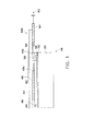
- FIG. 1 is a cross-sectional view of a touch display device according to an embodiment of the invention.
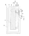
- FIG. 2A is a bottom view of a touch panel and a flexible circuit board of FIG. 1 .
- FIG. 2B is a partial enlarged bottom view of a touch control element of the touch panel of FIG. 2A according to another embodiment.
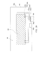
- FIG. 2C is a cross-sectional view of FIG. 2B along a line I-I.
- FIG. 3 is a bottom view of a touch panel and a flexible circuit board of FIG. 1 according to another embodiment.
- FIG. 4 is a bottom view of a touch panel and a flexible circuit board of FIG. 1 according to still another embodiment.
- FIG. 5 is a bottom view of a touch panel and a flexible circuit board of FIG. 1 according to yet another embodiment.
- FIG. 6 is a bottom view of a touch panel and a flexible circuit board of FIG. 1 according to still another embodiment.
- FIG. 1 is a cross-sectional view of a touch display device according to an embodiment of the invention.
- FIG. 2A is a bottom view of a touch panel and a flexible circuit board of FIG. 1 .
- the touch display device 100 includes a display panel 200, a shielding electrode layer 300, a touch panel 400a, a conductive element 500 and a flexible circuit board 600.
- the display panel 200 has a top surface 202.
- the display panel 200 is, for example, a transmissive display panel, a trans-reflective display panel, a reflective display panel, a vertical alignment (VA) display panel, an in plane switch (IPS) display panel, a multi-domain vertical alignment (MVA) display panel, a twist nematic (TN) display panel, a fringe field switching (FFS) display panel or an organic light-emitting diode (OLED) display panel, which is not limited by the invention.
- VA vertical alignment
- IPS in plane switch
- MVA multi-domain vertical alignment
- TN twist nematic
- FFS fringe field switching
- OLED organic light-emitting diode
- the shielding electrode layer 300 is disposed on the display panel 200, and covers the top surface 202 of the display panel 200, where a material of the shielding electrode layer 300 is, for example, a transparent conductive material, for example, indium tin oxide (ITO) or indium zinc oxide (IZO).
- a transparent conductive material for example, indium tin oxide (ITO) or indium zinc oxide (IZO).
- the touch panel 400a is disposed on the shielding electrode layer 300, and has a sensing region 402 and a peripheral region 404 surrounding the sensing region 402.
- the touch panel 400a includes a substrate 410, a touch control element 420a, at least one ground electrode 430a (only one ground electrode is schematically illustrated in FIG. 2A ) and at least one metal wire 440a (only one metal wire is schematically illustrated in FIG. 2A ).
- the touch control element 420a is disposed on an insulation layer 460 (referring to FIG.
- the touch control element 420a includes at least one sensing electrode 422 (a plurality of sensing electrodes is schematically illustrated in FIG. 2A ), at least one transmission wire 424 (a plurality of transmission wires is schematically illustrated in FIG. 2A ) and at least two pads 426a, where the pads 426a are a first pad 426a1 and at least one second pad 426a2 (a plurality of second pads is schematically illustrated in FIG. 2A ).
- the sensing electrodes 422 are located in the sensing region 402, and the transmission wires 424 and the pads 426a are located in the peripheral region 404, and the transmission wires 424 are located between the sensing electrodes 422 and the second pads 426a2, and are structurally and electrically connected to the sensing electrodes 422 and the second pads 426a2.
- the ground electrode 430a is disposed in the peripheral region 404 of the substrate 410.
- the meal wire 440a is disposed in the peripheral region 404 of the substrate 410, where the metal wire 440a is connected between the ground electrode 430a and the first pad 426a1.
- sensing electrodes 422 and a plurality of transmission wires 424 are illustrated in FIG. 2A , in other embodiments that are not illustrated, a single sensing electrode 422 or a single transmission wire 424 can also be used to construct the touch control element 420a of the touch panel 400a. Namely, the numbers of the sensing electrodes 422 and the transmission wires 424 are not limited to be one or plural. Moreover, a shape of the sensing electrode 422 is not limited to that illustrated in FIG. 2A .
- FIG. 2B is a partial bottom enlarged view of the touch control element of the touch panel of FIG. 2A according to another embodiment.
- FIG. 2C is a cross-sectional view of FIG. 2B along a line I-I.
- the sensing electrode 422a includes a plurality of first sensing series 423a (only one first sensing series is schematically illustrated in FIG. 2B ) and a plurality of second sensing series 425a (only one second sensing series is schematically illustrated in FIG. 2B ).
- Each of the first sensing series 423a extends along a first direction D1 and includes a plurality of first sensing electrode pads 423a1 and a plurality of first bridge electrodes 423a2 electrically connecting the first sensing electrode pads 423a1.
- Each of the second sensing series 425a extends along a second direction D2 and includes a plurality of second sensing electrode pads 425a1 and a plurality of second bridge electrodes 425a2 electrically connecting the second sensing electrode pads 425a1.
- Each of the second bridge electrodes 425a2 is insulated from the corresponding first bridge electrode 423a2 through an insulation layer 427.
- the first direction D1 is intersected with the second direction D2, and the first sensing series 423a and the second sensing series 425a are intersected with each other.
- a plurality of transmission wires 424a is disposed at peripheral of the first sensing series 423a and the second sensing series 425a, and each of the transmission wires 424a is connected to one of the first sensing series 423a and the second sensing series 425a, where the transmission wires 424a can be shielded by a light shielding layer 429.
- the ground electrode 430a (referring to FIG. 2A )
- the first sensing electrode pads 423a1 and the second sensing electrode pads 425a1 belong to a same film layer, i.e.
- the metal wire 440a (referring to FIG. 2A ), the second bridge electrodes 425a2, and the transmission wires 424a belong to a same film layer, i.e. the metal wire 440a, the second bridge electrodes 425a2 and the transmission wires 424a are simultaneously formed in a same fabricating process. In this way, fabrication cost is effectively saved.
- the sensing electrodes 422 can be a whole electrode layer formed in the sensing region 402, or can be electrode series formed by a plurality of diamond, rectangular and polygonal electrodes. Certainly, the sensing electrodes 422 can also be bar-shape electrodes formed in the sensing region 402.
- the touch panel 400a is, for example, a capacitive touch panel, an acoustic wave touch panel, an infrared touch panel or an optical touch panel, which is not limited by the invention.
- the conductive element 500 is disposed between the shielding electrode layer 300 and the touch panel 400a, where the shielding electrode layer 300 is structurally and electrically connected to the metal wire 440a or the ground electrode 430a of the touch panel 400a through the conductive element 500.
- the shielding electrode layer 300 is structurally and electrically connected to the metal wire 440a of the touch panel 400a through the conductive element 500.
- the conductive element 500 is, for example, a silver adhesive layer or a conductive adhesive tape.
- the flexible circuit board 600 is disposed on the touch panel 400a, and is located in the peripheral region 404, where the flexible circuit board 600 is electrically connected to the pads 426a of the touch control element 420a, so that the sensing electrode 422 and the metal wire 440a are electrically connected to the flexible circuit board 600 (referring to FIG. 2A ).
- the touch display device 100 of the present embodiment further includes an adhesive glue 700 disposed between the touch panel 400a and the shielding electrode layer 300, where a pattern of the adhesive glue 700 is, for example, a closed ring shape glue, and the touch panel 400a is fixed on the display panel 400a through the adhesion glue 700.
- the display panel 200 is coupled to the shielding electrode layer 300, so as to prevent the display panel 200 from coupling to the sensing electrode 422 in the touch panel 400a. In this way, an interference signal generated by the display panel 200 is prevented from influencing a touch signal sensed by the sensing electrode 422, so that sensing capability of the touch display device 100 is improved.
- the shielding electrode layer 300 of the present embodiment can transmit the static electricity between the touch panel 400a and the display panel 200 to the ground electrode 430a or the metal wire 440a of the touch panel 400a through the conductive element 500, and the metal wire 440a transmits the static electricity generated between the touch panel 400a and the display panel 200 to the ground through the electrical connection between the pad 426a and a ground terminal 602 of the flexible circuit board 600.
- the static electricity is effectively discharged to protect the electronic components (not shown) inside the touch display device 100.
- the numbers and patterns of the ground electrodes 430a and the metal wires 440a of the touch panel 400a are not limited by the invention, and in the present embodiment, the number of the ground electrode 430a is one and a shape thereof is a rectangle, and the number of the metal wire 440a is one and the metal wire 440a is only located between the ground electrode 430a and the pad 426a.
- a plurality of embodiments is provided below to describe touch panels 400b, 400c, 400d and 400e. It should be noticed that the referential numbers and a part of content of the aforementioned embodiment are adopted in the following embodiments, in which the same reference numbers denote the same or like components, and descriptions of the same technical contents are omitted. The aforementioned embodiment can be referred for descriptions of the omitted part, and details thereof are not repeated.
- FIG. 3 is a bottom view of the touch panel and the flexible circuit board of FIG. 1 according to another embodiment.
- the touch panel 400b of the present embodiment is similar to the touch panel 400a of FIG. 2A , and a main difference there between is that a ground electrode 430b of the touch panel 400b of the present embodiment includes a first ground electrode 432b and a second ground electrode 434b, the metal wire 440b includes a first metal wire 442b and a second metal wire 444b, and the pads 426b includes a first pad 426b1. a second pad 426b2 and at least one third pad 426b3 (a plurality of the third pad is schematically illustrated in FIG.
- the first metal wire 442b is electrically connected to the first ground electrode 432b and the first pad 426b1
- the second metal wire 444b is electrically connected to the second ground electrode 434b and the second pad 426b2.
- the transmission lines 424 of the touch control element 420b are electrically connected to the third pads 426b3.
- FIG. 4 is a bottom view of the touch panel and the flexible circuit board of FIG. 1 according to still another embodiment.
- the touch panel 400c of the present embodiment is similar to the touch panel 400a of FIG. 2A , and a main difference there between is that a ground electrode 430c of the touch panel 400c of the present embodiment is a ring-shape electrode, which surrounds the sensing region 402 and has a first end 433c and a second end 435c opposite to each other.
- the metal wire 440c includes a first metal wire 442c and a second metal wire 444c.
- the pads 426c include a first pad 426c1, a second pad 426c2 and at least one third pad 426c3 (a plurality of the third pad is schematically illustrated in FIG. 4 ) located between the first pad 426c1 and the second pad 426c2.
- the first metal wire 442c is electrically connected to the first end 433c of the ring-shape ground electrode 430c and the first pad 426c1
- the second metal wire 444c is electrically connected to the second end 435c of the ring-shape ground electrode 430c and the second pad 426c2.
- the transmission wires 424 of the touch control element 420c are connected to the third pads 426c3.
- FIG. 5 is a bottom view of the touch panel and the flexible circuit board of FIG. 1 according to yet another embodiment.
- the touch panel 400d of the present embodiment is similar to the touch panel 400a of FIG. 2A , and a main difference there between is that a ground electrode 430d of the touch panel 400d of the present embodiment includes a first type ring-shape ground electrode 432d and a second type ring-shape ground electrode 434d.
- the first type ring-shape ground electrode 432d and the second type ring-shape ground electrode 434d surround the sensing region 402, and the first type ring-shape ground electrode 432d has a first end 433d and a second end 435d opposite to each other, and the second type ring-shape ground electrode 434d has a third end 437d and a fourth end 439d opposite to each other.
- the metal wire 440d includes a first metal wire 442d and a second metal wire 444d.
- the pads 426d include a first pad 426d1, a second pad 426d2 and at least one third pad 426d3 (a plurality of the third pad is schematically illustrated in FIG.
- the first metal wire 442d is electrically connected to the first end 433d of the first type ring-shape ground electrode 432d and the first pad 426d1
- the second metal wire 444d is electrically connected to the third end 437d of the second type ring-shape ground electrode 434d and the second pad 426d2.
- the second end 435d of the first type ring-shape ground electrode 432d is adjacent to the fourth end 439d of the second type ring-shape ground electrode 434d.
- the transmission wires 424 of the touch control element 420d are connected to the third pads 426d3.
- FIG. 6 is a bottom view of the touch panel and the flexible circuit board of FIG. 1 according to still another embodiment.
- the touch panel 400e of the present embodiment is similar to the touch panel 400a of FIG. 2A , and a main difference there between is that a ground electrode 430e of the touch panel 400e of the present embodiment includes a first ground electrode 432e and a second ground electrode 434e.
- the metal wire 440e includes a first metal wire 442e, a second metal wire 444e and a third metal wire 446e.
- the pads 426e include a first pad 426e1, a second pad 426e2 and at least one third pad 426e3 (a plurality of the third pad is schematically illustrated in FIG.
- the first metal wire 442e is electrically connected to the first ground electrode 432e and the first pad 426e1
- the second metal wire 444e is electrically connected to the second ground electrode 434e and the second pad 426e2.
- the third metal wire 446e is electrically connected to the first ground electrode 432e and the second ground electrode 434e and surrounds the sensing region 404.
- the transmission wires 424 of the touch control element 420e are connected to the third pads 426e3.
- the shielding electrode layer is disposed between the touch panel and the display panel, which may mitigate signal interference between the touch panel and the display panel. Moreover, the shielding electrode layer can transmit the static electricity between the touch panel and the display panel to the ground electrode or the metal wire of the touch panel through the conductive element, and the metal wire transmits the static electricity generated between the touch panel and the display panel to the ground through the electrical connection between the pad and the ground terminal of the flexible circuit board. In this way, not only sensing capability of the touch display device is effectively improved, but also the static electricity is effectively discharged to protect the electronic components inside the touch display device.
Landscapes
- Engineering & Computer Science (AREA)
- General Engineering & Computer Science (AREA)
- Theoretical Computer Science (AREA)
- Human Computer Interaction (AREA)
- Physics & Mathematics (AREA)
- General Physics & Mathematics (AREA)
- Position Input By Displaying (AREA)
- Devices For Indicating Variable Information By Combining Individual Elements (AREA)
Applications Claiming Priority (1)
| Application Number | Priority Date | Filing Date | Title |
|---|---|---|---|
| CN2012100520651A CN103294238A (zh) | 2012-03-01 | 2012-03-01 | 触控显示装置 |
Publications (2)
| Publication Number | Publication Date |
|---|---|
| EP2634677A2 true EP2634677A2 (de) | 2013-09-04 |
| EP2634677A3 EP2634677A3 (de) | 2016-07-13 |
Family
ID=46639306
Family Applications (1)
| Application Number | Title | Priority Date | Filing Date |
|---|---|---|---|
| EP12175084.8A Withdrawn EP2634677A3 (de) | 2012-03-01 | 2012-07-05 | Berührungsanzeigevorrichtung |
Country Status (3)
| Country | Link |
|---|---|
| US (1) | US20130229364A1 (de) |
| EP (1) | EP2634677A3 (de) |
| CN (1) | CN103294238A (de) |
Families Citing this family (36)
| Publication number | Priority date | Publication date | Assignee | Title |
|---|---|---|---|---|
| KR101960532B1 (ko) * | 2012-04-19 | 2019-03-20 | 엘지디스플레이 주식회사 | 표시장치용 정전용량 방식 터치 스크린 패널 및 그 제조방법 |
| US9609736B2 (en) * | 2012-06-29 | 2017-03-28 | Lg Innotek Co., Ltd. | Touch panel and method of manufacturing the same |
| TWI492111B (zh) * | 2012-10-02 | 2015-07-11 | 傑聖科技股份有限公司 | 觸控面板及其製造方法 |
| CN103809796B (zh) * | 2012-11-09 | 2018-03-16 | 宝宸(厦门)光学科技有限公司 | 触控感应电极结构及其制造方法 |
| US9348453B2 (en) * | 2013-02-04 | 2016-05-24 | Nokia Technologies Oy | Touch sensing arrangement with first and second shield electrodes |
| TWM457919U (zh) * | 2013-02-08 | 2013-07-21 | Liyitec Inc | 觸控面板 |
| WO2014192336A1 (ja) * | 2013-05-29 | 2014-12-04 | シャープ株式会社 | タッチパネル基板 |
| TW201447666A (zh) * | 2013-06-13 | 2014-12-16 | Wintek Corp | 觸控面板 |
| TWI485598B (zh) * | 2013-07-02 | 2015-05-21 | Au Optronics Corp | 觸控面板及其製造方法 |
| TW201508568A (zh) * | 2013-08-16 | 2015-03-01 | Wintek Corp | 觸控顯示裝置 |
| US9367155B2 (en) * | 2013-10-01 | 2016-06-14 | Htc Corporation | Touch panel assembly and electronic device |
| KR102175563B1 (ko) * | 2013-11-13 | 2020-11-06 | 엘지이노텍 주식회사 | 터치 패널 |
| KR102275876B1 (ko) * | 2014-04-01 | 2021-07-12 | 엘지이노텍 주식회사 | 터치 패널 및 이를 포함하는 터치 디바이스 |
| KR102187807B1 (ko) * | 2014-04-17 | 2020-12-07 | 엘지이노텍 주식회사 | 터치 패널 및 이를 포함하는 터치 디바이스 |
| CN103955312A (zh) * | 2014-05-06 | 2014-07-30 | 山东华芯富创电子科技有限公司 | 一种触控面板防静电结构及其制作方法 |
| US9535521B2 (en) * | 2014-11-21 | 2017-01-03 | Interface Optoelectronics Corporation | Touch panel |
| CN105700725B (zh) * | 2014-11-27 | 2018-11-02 | 林志忠 | 触控面板结构 |
| KR20160092360A (ko) | 2015-01-27 | 2016-08-04 | 삼성전자주식회사 | 스타일러스 펜 및 터치 패널 |
| CN105093607B (zh) * | 2015-05-08 | 2018-01-09 | 上海天马微电子有限公司 | 阵列基板、触控显示面板以及触控显示装置 |
| CN105117073B (zh) | 2015-09-29 | 2019-02-26 | 京东方科技集团股份有限公司 | 一种触控显示面板和触控显示装置 |
| KR20170039025A (ko) * | 2015-09-30 | 2017-04-10 | 삼성디스플레이 주식회사 | 표시 장치 |
| CN111399681B (zh) * | 2015-12-16 | 2023-06-16 | 瀚宇彩晶股份有限公司 | 触控面板与电子装置 |
| CN105607780B (zh) * | 2016-03-14 | 2019-02-26 | 京东方科技集团股份有限公司 | 静电放电电路、具有静电放电电路的显示面板和静电放电方法 |
| CN106371669B (zh) * | 2016-09-28 | 2020-01-21 | 厦门天马微电子有限公司 | 触控显示面板和触控显示装置 |
| CN107783699B (zh) * | 2017-10-16 | 2021-05-04 | 业成科技(成都)有限公司 | 触控面板结构与其制造方法 |
| KR102467874B1 (ko) * | 2017-10-16 | 2022-11-16 | 삼성디스플레이 주식회사 | 표시 장치 |
| CN109023849B (zh) * | 2018-09-28 | 2023-09-15 | 重庆海尔滚筒洗衣机有限公司 | 一种控制面板及洗衣机 |
| CN109508115B (zh) | 2018-12-04 | 2020-12-04 | 武汉华星光电半导体显示技术有限公司 | 触控面板及显示装置 |
| CN110703931B (zh) * | 2019-04-16 | 2023-06-06 | 光宝电子(广州)有限公司 | 滑鼠 |
| TWI704482B (zh) * | 2019-12-06 | 2020-09-11 | 友達光電股份有限公司 | 顯示裝置 |
| CN110928078B (zh) * | 2019-12-12 | 2022-07-12 | 厦门天马微电子有限公司 | 一种显示面板及其制备方法、显示装置 |
| CN110888558B (zh) * | 2020-01-02 | 2024-01-02 | 业成科技(成都)有限公司 | 触控面板和触控装置 |
| JP7321112B2 (ja) * | 2020-02-10 | 2023-08-04 | 三菱電機株式会社 | タッチパネルおよびこれを備えた表示装置 |
| CN113301710B (zh) * | 2020-02-24 | 2022-09-09 | 京东方科技集团股份有限公司 | 显示装置及其制备方法 |
| CN116643666A (zh) * | 2022-02-16 | 2023-08-25 | 川奇光电科技(扬州)有限公司 | 触控显示装置 |
| TWI810817B (zh) * | 2022-02-16 | 2023-08-01 | 元太科技工業股份有限公司 | 觸控顯示裝置 |
Family Cites Families (7)
| Publication number | Priority date | Publication date | Assignee | Title |
|---|---|---|---|---|
| JP2009086184A (ja) * | 2007-09-28 | 2009-04-23 | Casio Comput Co Ltd | タッチパネル付き液晶表示装置 |
| CN101452128B (zh) * | 2007-12-05 | 2012-03-14 | 群康科技(深圳)有限公司 | 触控显示装置和电子装置 |
| KR101237640B1 (ko) * | 2008-01-29 | 2013-02-27 | (주)멜파스 | 기생 캐패시턴스 방지 구조를 구비한 터치스크린 장치 |
| KR101706232B1 (ko) * | 2010-06-29 | 2017-02-15 | 엘지디스플레이 주식회사 | 터치 패널 |
| TW201205398A (en) * | 2010-07-30 | 2012-02-01 | Chimei Innolux Corp | Display system having capacitive touch panel and manufacturing method thereof |
| US8923014B2 (en) * | 2010-08-19 | 2014-12-30 | Lg Display Co., Ltd. | Display device having touch panel |
| US20120326992A1 (en) * | 2011-06-27 | 2012-12-27 | Silicon Integrated Systems Corp. | Touch Panel for Providing a Shield Against Noise |
-
2012
- 2012-03-01 CN CN2012100520651A patent/CN103294238A/zh active Pending
- 2012-06-15 US US13/523,908 patent/US20130229364A1/en not_active Abandoned
- 2012-07-05 EP EP12175084.8A patent/EP2634677A3/de not_active Withdrawn
Non-Patent Citations (1)
| Title |
|---|
| None |
Also Published As
| Publication number | Publication date |
|---|---|
| EP2634677A3 (de) | 2016-07-13 |
| US20130229364A1 (en) | 2013-09-05 |
| CN103294238A (zh) | 2013-09-11 |
Similar Documents
| Publication | Publication Date | Title |
|---|---|---|
| EP2634677A2 (de) | Berührungsanzeigevorrichtung | |
| TWI471642B (zh) | Touch panel structure and its touch display panel | |
| US8730195B2 (en) | Touch-sensitive device and touch-sensitive display device | |
| JP5300684B2 (ja) | 静電容量型入力装置、静電容量型入力装置の製造方法、および入力機能付き電気光学装置 | |
| JP5300640B2 (ja) | 静電容量型入力装置および入力装置付き電気光学装置 | |
| US9239656B2 (en) | Touch display device and method of manufacturing the same | |
| TWI390280B (zh) | 觸控面板顯示器與觸控顯示裝置 | |
| CN102446012B (zh) | 电容式触控面板结构及触控显示面板 | |
| CN103927032B (zh) | 触控显示装置 | |
| TW201403171A (zh) | 觸控感測結構 | |
| TWI550483B (zh) | Anti-static touch panel | |
| TWI665592B (zh) | 觸控顯示裝置 | |
| TWI630537B (zh) | 具有壓力感測的觸控顯示系統 | |
| TW201530400A (zh) | 觸控裝置 | |
| KR102119827B1 (ko) | 터치 패널 | |
| CN104111755A (zh) | 一种触控结构、触控面板及触控装置 | |
| US20170025480A1 (en) | In-cell touch panel | |
| US20130069892A1 (en) | Touch-sensitive device and touch-sensitive display device | |
| US9188803B2 (en) | Touch panel | |
| KR101900333B1 (ko) | 연성 회로기판 및 이를 이용한 자기-정전용량형 터치 패널 | |
| CN106886325B (zh) | 触控面板与电子装置 | |
| TWI567613B (zh) | 壓力感測模組以及壓力觸控感測顯示模組 | |
| CN103699250A (zh) | 触控显示模块及手持电子装置 | |
| TWI396004B (zh) | 電子裝置 | |
| TW201723776A (zh) | 觸控面板與電子裝置 |
Legal Events
| Date | Code | Title | Description |
|---|---|---|---|
| PUAI | Public reference made under article 153(3) epc to a published international application that has entered the european phase |
Free format text: ORIGINAL CODE: 0009012 |
|
| AK | Designated contracting states |
Kind code of ref document: A2 Designated state(s): AL AT BE BG CH CY CZ DE DK EE ES FI FR GB GR HR HU IE IS IT LI LT LU LV MC MK MT NL NO PL PT RO RS SE SI SK SM TR |
|
| AX | Request for extension of the european patent |
Extension state: BA ME |
|
| PUAL | Search report despatched |
Free format text: ORIGINAL CODE: 0009013 |
|
| AK | Designated contracting states |
Kind code of ref document: A3 Designated state(s): AL AT BE BG CH CY CZ DE DK EE ES FI FR GB GR HR HU IE IS IT LI LT LU LV MC MK MT NL NO PL PT RO RS SE SI SK SM TR |
|
| AX | Request for extension of the european patent |
Extension state: BA ME |
|
| RIC1 | Information provided on ipc code assigned before grant |
Ipc: G06F 3/044 20060101AFI20160603BHEP |
|
| STAA | Information on the status of an ep patent application or granted ep patent |
Free format text: STATUS: THE APPLICATION HAS BEEN PUBLISHED |
|
| STAA | Information on the status of an ep patent application or granted ep patent |
Free format text: STATUS: THE APPLICATION IS DEEMED TO BE WITHDRAWN |
|
| 18D | Application deemed to be withdrawn |
Effective date: 20170114 |