EP2634813A1 - Electrode et son procédé de fabrication - Google Patents
Electrode et son procédé de fabrication Download PDFInfo
- Publication number
- EP2634813A1 EP2634813A1 EP11833584.3A EP11833584A EP2634813A1 EP 2634813 A1 EP2634813 A1 EP 2634813A1 EP 11833584 A EP11833584 A EP 11833584A EP 2634813 A1 EP2634813 A1 EP 2634813A1
- Authority
- EP
- European Patent Office
- Prior art keywords
- electrode
- thin film
- film layer
- metallic thin
- micro
- Prior art date
- Legal status (The legal status is an assumption and is not a legal conclusion. Google has not performed a legal analysis and makes no representation as to the accuracy of the status listed.)
- Withdrawn
Links
- 238000004519 manufacturing process Methods 0.000 title description 5
- 239000010409 thin film Substances 0.000 claims abstract description 80
- 238000002834 transmittance Methods 0.000 claims abstract description 16
- 238000000034 method Methods 0.000 claims description 43
- 239000004005 microsphere Substances 0.000 claims description 43
- 230000031700 light absorption Effects 0.000 claims description 33
- 239000000463 material Substances 0.000 claims description 29
- 239000000758 substrate Substances 0.000 claims description 26
- VYPSYNLAJGMNEJ-UHFFFAOYSA-N Silicium dioxide Chemical compound O=[Si]=O VYPSYNLAJGMNEJ-UHFFFAOYSA-N 0.000 claims description 19
- 239000004793 Polystyrene Substances 0.000 claims description 16
- 239000002184 metal Substances 0.000 claims description 16
- 229910052751 metal Inorganic materials 0.000 claims description 16
- 229920002223 polystyrene Polymers 0.000 claims description 16
- 235000012239 silicon dioxide Nutrition 0.000 claims description 15
- 238000000151 deposition Methods 0.000 claims description 9
- 238000005530 etching Methods 0.000 claims description 6
- 238000001459 lithography Methods 0.000 claims description 6
- 230000003746 surface roughness Effects 0.000 claims description 6
- 239000000377 silicon dioxide Substances 0.000 claims description 4
- 229910004613 CdTe Inorganic materials 0.000 claims description 3
- 229910001218 Gallium arsenide Inorganic materials 0.000 claims description 3
- BERDEBHAJNAUOM-UHFFFAOYSA-N copper(I) oxide Inorganic materials [Cu]O[Cu] BERDEBHAJNAUOM-UHFFFAOYSA-N 0.000 claims description 3
- KRFJLUBVMFXRPN-UHFFFAOYSA-N cuprous oxide Chemical compound [O-2].[Cu+].[Cu+] KRFJLUBVMFXRPN-UHFFFAOYSA-N 0.000 claims description 3
- 238000000059 patterning Methods 0.000 claims description 2
- 230000005540 biological transmission Effects 0.000 claims 1
- 239000010408 film Substances 0.000 abstract description 33
- 230000005693 optoelectronics Effects 0.000 abstract description 4
- 239000010410 layer Substances 0.000 description 86
- 239000010453 quartz Substances 0.000 description 11
- 238000010586 diagram Methods 0.000 description 10
- XLOMVQKBTHCTTD-UHFFFAOYSA-N Zinc monoxide Chemical compound [Zn]=O XLOMVQKBTHCTTD-UHFFFAOYSA-N 0.000 description 8
- 238000002835 absorbance Methods 0.000 description 8
- 238000010521 absorption reaction Methods 0.000 description 8
- XUIMIQQOPSSXEZ-UHFFFAOYSA-N Silicon Chemical compound [Si] XUIMIQQOPSSXEZ-UHFFFAOYSA-N 0.000 description 6
- 238000000206 photolithography Methods 0.000 description 6
- 229910052710 silicon Inorganic materials 0.000 description 6
- 239000010703 silicon Substances 0.000 description 6
- 239000006096 absorbing agent Substances 0.000 description 5
- 238000005516 engineering process Methods 0.000 description 5
- 239000010931 gold Substances 0.000 description 5
- 238000001883 metal evaporation Methods 0.000 description 5
- 229910021417 amorphous silicon Inorganic materials 0.000 description 4
- 239000002077 nanosphere Substances 0.000 description 4
- 238000000054 nanosphere lithography Methods 0.000 description 4
- 238000001020 plasma etching Methods 0.000 description 4
- 239000004065 semiconductor Substances 0.000 description 4
- XLYOFNOQVPJJNP-UHFFFAOYSA-N water Substances O XLYOFNOQVPJJNP-UHFFFAOYSA-N 0.000 description 4
- 239000011787 zinc oxide Substances 0.000 description 4
- 239000013078 crystal Substances 0.000 description 3
- 229910021424 microcrystalline silicon Inorganic materials 0.000 description 3
- 230000003287 optical effect Effects 0.000 description 3
- 238000001878 scanning electron micrograph Methods 0.000 description 3
- 238000006243 chemical reaction Methods 0.000 description 2
- 229910021419 crystalline silicon Inorganic materials 0.000 description 2
- 230000007547 defect Effects 0.000 description 2
- 230000008021 deposition Effects 0.000 description 2
- 230000002542 deteriorative effect Effects 0.000 description 2
- 230000000694 effects Effects 0.000 description 2
- 239000011521 glass Substances 0.000 description 2
- PCHJSUWPFVWCPO-UHFFFAOYSA-N gold Chemical compound [Au] PCHJSUWPFVWCPO-UHFFFAOYSA-N 0.000 description 2
- 229910052737 gold Inorganic materials 0.000 description 2
- 238000012986 modification Methods 0.000 description 2
- 230000004048 modification Effects 0.000 description 2
- 238000009304 pastoral farming Methods 0.000 description 2
- 229910021420 polycrystalline silicon Inorganic materials 0.000 description 2
- 239000002994 raw material Substances 0.000 description 2
- 238000011946 reduction process Methods 0.000 description 2
- 239000000126 substance Substances 0.000 description 2
- 239000011701 zinc Substances 0.000 description 2
- MARUHZGHZWCEQU-UHFFFAOYSA-N 5-phenyl-2h-tetrazole Chemical compound C1=CC=CC=C1C1=NNN=N1 MARUHZGHZWCEQU-UHFFFAOYSA-N 0.000 description 1
- ZOXJGFHDIHLPTG-UHFFFAOYSA-N Boron Chemical compound [B] ZOXJGFHDIHLPTG-UHFFFAOYSA-N 0.000 description 1
- MCEWYIDBDVPMES-UHFFFAOYSA-N [60]pcbm Chemical compound C123C(C4=C5C6=C7C8=C9C%10=C%11C%12=C%13C%14=C%15C%16=C%17C%18=C(C=%19C=%20C%18=C%18C%16=C%13C%13=C%11C9=C9C7=C(C=%20C9=C%13%18)C(C7=%19)=C96)C6=C%11C%17=C%15C%13=C%15C%14=C%12C%12=C%10C%10=C85)=C9C7=C6C2=C%11C%13=C2C%15=C%12C%10=C4C23C1(CCCC(=O)OC)C1=CC=CC=C1 MCEWYIDBDVPMES-UHFFFAOYSA-N 0.000 description 1
- 239000011358 absorbing material Substances 0.000 description 1
- 229910052796 boron Inorganic materials 0.000 description 1
- 239000003245 coal Substances 0.000 description 1
- 150000001875 compounds Chemical class 0.000 description 1
- UIPVMGDJUWUZEI-UHFFFAOYSA-N copper;selanylideneindium Chemical compound [Cu].[In]=[Se] UIPVMGDJUWUZEI-UHFFFAOYSA-N 0.000 description 1
- 230000003247 decreasing effect Effects 0.000 description 1
- 230000002939 deleterious effect Effects 0.000 description 1
- 230000006866 deterioration Effects 0.000 description 1
- 230000005684 electric field Effects 0.000 description 1
- 238000001704 evaporation Methods 0.000 description 1
- 229910010272 inorganic material Inorganic materials 0.000 description 1
- 239000011147 inorganic material Substances 0.000 description 1
- 238000005259 measurement Methods 0.000 description 1
- 229910021421 monocrystalline silicon Inorganic materials 0.000 description 1
- 239000003208 petroleum Substances 0.000 description 1
- 239000002096 quantum dot Substances 0.000 description 1
- 230000005855 radiation Effects 0.000 description 1
- 238000005215 recombination Methods 0.000 description 1
- 230000006798 recombination Effects 0.000 description 1
- 239000002356 single layer Substances 0.000 description 1
- 238000001228 spectrum Methods 0.000 description 1
- 238000003860 storage Methods 0.000 description 1
- 235000012431 wafers Nutrition 0.000 description 1
Images


Classifications
-
- H—ELECTRICITY
- H10—SEMICONDUCTOR DEVICES; ELECTRIC SOLID-STATE DEVICES NOT OTHERWISE PROVIDED FOR
- H10F—INORGANIC SEMICONDUCTOR DEVICES SENSITIVE TO INFRARED RADIATION, LIGHT, ELECTROMAGNETIC RADIATION OF SHORTER WAVELENGTH OR CORPUSCULAR RADIATION
- H10F71/00—Manufacture or treatment of devices covered by this subclass
-
- H—ELECTRICITY
- H10—SEMICONDUCTOR DEVICES; ELECTRIC SOLID-STATE DEVICES NOT OTHERWISE PROVIDED FOR
- H10F—INORGANIC SEMICONDUCTOR DEVICES SENSITIVE TO INFRARED RADIATION, LIGHT, ELECTROMAGNETIC RADIATION OF SHORTER WAVELENGTH OR CORPUSCULAR RADIATION
- H10F77/00—Constructional details of devices covered by this subclass
- H10F77/20—Electrodes
- H10F77/244—Electrodes made of transparent conductive layers, e.g. transparent conductive oxide [TCO] layers
- H10F77/254—Electrodes made of transparent conductive layers, e.g. transparent conductive oxide [TCO] layers comprising a metal, e.g. transparent gold
-
- H—ELECTRICITY
- H10—SEMICONDUCTOR DEVICES; ELECTRIC SOLID-STATE DEVICES NOT OTHERWISE PROVIDED FOR
- H10F—INORGANIC SEMICONDUCTOR DEVICES SENSITIVE TO INFRARED RADIATION, LIGHT, ELECTROMAGNETIC RADIATION OF SHORTER WAVELENGTH OR CORPUSCULAR RADIATION
- H10F71/00—Manufacture or treatment of devices covered by this subclass
- H10F71/138—Manufacture of transparent electrodes, e.g. transparent conductive oxides [TCO] or indium tin oxide [ITO] electrodes
-
- H—ELECTRICITY
- H10—SEMICONDUCTOR DEVICES; ELECTRIC SOLID-STATE DEVICES NOT OTHERWISE PROVIDED FOR
- H10F—INORGANIC SEMICONDUCTOR DEVICES SENSITIVE TO INFRARED RADIATION, LIGHT, ELECTROMAGNETIC RADIATION OF SHORTER WAVELENGTH OR CORPUSCULAR RADIATION
- H10F77/00—Constructional details of devices covered by this subclass
- H10F77/20—Electrodes
-
- H—ELECTRICITY
- H10—SEMICONDUCTOR DEVICES; ELECTRIC SOLID-STATE DEVICES NOT OTHERWISE PROVIDED FOR
- H10K—ORGANIC ELECTRIC SOLID-STATE DEVICES
- H10K30/00—Organic devices sensitive to infrared radiation, light, electromagnetic radiation of shorter wavelength or corpuscular radiation
- H10K30/80—Constructional details
- H10K30/81—Electrodes
- H10K30/82—Transparent electrodes, e.g. indium tin oxide [ITO] electrodes
- H10K30/83—Transparent electrodes, e.g. indium tin oxide [ITO] electrodes comprising arrangements for extracting the current from the cell, e.g. metal finger grid systems to reduce the serial resistance of transparent electrodes
-
- Y—GENERAL TAGGING OF NEW TECHNOLOGICAL DEVELOPMENTS; GENERAL TAGGING OF CROSS-SECTIONAL TECHNOLOGIES SPANNING OVER SEVERAL SECTIONS OF THE IPC; TECHNICAL SUBJECTS COVERED BY FORMER USPC CROSS-REFERENCE ART COLLECTIONS [XRACs] AND DIGESTS
- Y02—TECHNOLOGIES OR APPLICATIONS FOR MITIGATION OR ADAPTATION AGAINST CLIMATE CHANGE
- Y02E—REDUCTION OF GREENHOUSE GAS [GHG] EMISSIONS, RELATED TO ENERGY GENERATION, TRANSMISSION OR DISTRIBUTION
- Y02E10/00—Energy generation through renewable energy sources
- Y02E10/50—Photovoltaic [PV] energy
Definitions
- the present invention relates to fields of photovoltaic applications and optoelectronic applications, and more particularly, to an electrode for photovoltaic applications or optoelectronic applications and a fabricating method thereof.
- the core of a solar cell is P-N junction. Electron-hole pairs are generated when sunlight with energy higher than semiconductor's band gap energy is incident on the P-N junction of a solar cell. With the electric field generated on the P-N junction, electrons are transported to N layer, and holes are transported to P layer at the same time, thereby resulting in photoelectric effect between the P and N layers. When two terminals of the solar cell are connected to a load or system, electric energy in the form of current will be generated.
- Solar cells are classified into various types in terms of materials for forming intrinsic layers, i.e., light absorption layers.
- silicon solar cells with intrinsic layers made from silicon are the most common type.
- CIS, CuInSe 2 copper-indium-selenium
- III-V materials based solar cells dye-sensitized solar cells and organic solar cells, etc.
- Solar cells with a single-crystalline silicon substrate have significantly higher conversion efficiency compared to other types of solar cells.
- their fatal defect is a high fabricating cost due to use of single-crystalline silicon wafers.
- polycrystalline silicon solar cells may be produced with relatively low fabricating cost, however, polycrystalline silicon solar cells and monocrystalline silicon solar cells do not differ significantly, since these two types of solar cells are both made from a large amount of raw materials. Therefore, their high price of raw material and complex fabricating process make it difficult to reduce fabricating cost.
- thin film silicon solar cells As one solution for addressing the defects of these crystal solar cells, thin film silicon solar cells have obtained much attention because of their very low fabricating cost, since they are fabricated by depositing silicon films on glass as the absorption layers. In fact, thin film silicon solar cells may be made 100 times thinner than crystal ones.
- Thin film solar cells are fabricated by sequentially performing the following steps: forming a front (back) electrode on a substrate made of glass, forming a semiconductor layer on the front (back) electrode and forming a back (front) electrode on the semiconductor layer.
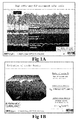
- Fig.1A shows a scanning electron microscope (SEM) image of a solar cell which employs this technology and a schematics view of the solar cell.
- Fig. 1B shows an image of a ⁇ c -Si:H film grown on a textured ZnO film.
- Fig. 1A gray regions in the SEM image indicate highly textured ZnO:B (boron doped zinc oxide) film.
- the two black regions indicate two PIN junctions (a-Si:H on the top, and ⁇ c-Si:H at the bottom). It is clear from Fig, 1A that surfaces of both PIN junction films are uneven, resulting in a rough and textured surface of the lower layer. With this regard, it can be more clearly seen from Fig. 1B .
- This texture-induced roughness of junction surface has a deleterious influence on the junction quality, such as a low shunt resistance, a high dark current, a high carrier recombination rate, a low fill factor and a low open circuit voltage, and therefore lowers the energy conversion efficiency and reliability of the solar cells.
- this light trapping scheme is not efficient in the frequency ranges closely above the band gap energy of the absorber (i.e. near infrared frequencies), making light in these frequency ranges mainly being absorbed by the absorber.
- SWE optical radiation induced performance deterioration
- deposition of textured TCO films also involves a high temperature and a high cost.
- an object of the present invention is to provide an electrode and a manufacturing method thereof, which may not use or use little transparent conductive oxide films while manufacturing the electrode, and doesn't need a piling process, thereby preventing junction quality from deteriorating due to the piled conductive oxide thick film.
- the planar electrode may be used as a window superstrate, allowing for a high quality planar PV junction to be deposited over it.
- Another object of the present invention is to provide another electrode and a fabricating method thereof, with which texturing process for back electrodes is not required when manufacturing solar cells.
- an electrode including a substantially planar metallic thin film layer with a patterned structure, which is configured to transmit an incident light through the metallic thin film layer.
- the patterned structure may be an Escheric series of patterns.
- the patterned structure may include an array of circular holes.
- circular holes in the array of circular holes may be periodically distributed or randomly distributed.
- the patterned structure may include a plurality of parallel lines.
- the patterned structure may include a plurality of crossed lines.
- the parallel lines or crossed lines may be periodically distributed or randomly distributed.
- the metallic thin film layer may be transmittable for a visible light, a near infrared light or an infrared light.
- the planar metallic thin film layer may have a surface roughness less than 1 ⁇ m, 100nm, 10nm or 1nm.
- a material for forming the planar metallic thin film layer may have a resistivity less than 0.005, 0.002 or 0.001 ⁇ m .
- the metallic thin film layer may be fabricated with a microsphere lithography process.
- a sheet resistance of the metallic thin film layer may be given by: R sq ⁇ ⁇ d ⁇ 1 - r R - 1 wherein, R sq is the sheet resistance of the metallic thin film layer, ⁇ is a resistivity of the material for forming the metallic thin film layer, d is a thickness of the metallic thin film layer, R is a radius of the microspheres prior to the microsphere lithography process, and r is a microsphere radius after the microsphere radius reduction.
- the microspheres may be made from polystyrene, or may be made from inorganic materials such as silicon dioxide.
- d has a value ranging from 5 ⁇ 1000nm
- R has a value ranging from 10nm ⁇ 10 ⁇ m
- r ⁇ R has a value ranging from 5 ⁇ 1000nm
- d has a value ranging from 5 ⁇ 1000nm
- R has a value ranging from 10nm ⁇ 10 ⁇ m
- r ⁇ R has a value ranging from 10nm ⁇ 10 ⁇ m
- a method for fabricating an electrode comprising: depositing organic microspheres on a substrate; etching back the organic microspheres to expose a portion of a surface of the substrate; depositing metal on the microspheres and the exposed substrate surface; peeling off the microspheres to form a metallic conductive thin film layer with a patterned structure, wherein the metallic conductive thin film layer is configured to transmit an incident light through the metallic conductive thin film layer.
- the patterned structure may include an array of circular holes, a plurality of parallel lines or a plurality of crossed lines.
- an electrode laminated on a light absorption layer comprising a planar metallic thin film layer pattern comprising at least a first micro-strip array with a first size and a first shape, wherein the planar metallic thin film layer pattern is configured to transmit an incident light in a first wavelength range into the light absorption layer, and wherein the first wavelength range is determined at least partly based on the first size and the first shape of the first micro-strip array.
- the planar metallic thin film layer pattern may further include a second micro-strip array with a second size and a second shape, and a third micro-strip array with a third size and a third shape, wherein the planar metallic thin film layer pattern is configured to transmit an incident light in a second wavelength range and an incident light in a third wavelength range into the light absorption layer, and wherein the second wavelength range is determined at least partly based on the second size and the second shape of the second micro-strip array, and the third wavelength range is determined at least partly based on the third size and the third shape of the third micro-strip array.
- the light absorption material layer may include a PN junction, a PIN junction or a plurality of junctions.
- the light absorption material may include a photovoltaic material.
- the light absorption material may include one of Si, CIGS, CIS, CdTe, GaAs, Cu 2 O, Zn 3 P 2 and SiC.
- the micro-strip may be of rectangle.
- planar metallic thin film layer may have a surface roughness less than 1 ⁇ m, 100nm, 10nm or 1nm.
- the material for forming the planar metallic thin film layer may have a resistivity less than 0.005, 0.002 or 0.001 ⁇ m .
- a method for fabricating an electrode comprising: depositing a metal layer on a light absorption layer; patterning the metallic layer to form a planar metallic thin film layer pattern comprising at least a first micro-strip array with a first size and a first shape, wherein the planar metallic thin film layer pattern is configured to transmit an incident light in a first wavelength range into the light absorption layer, and wherein the first wavelength range is determined at least partly based on the first size and the first shape of the first micro-strip array.
- Fig.1A shows a scanning electron microscope (SEM) image of a solar cell which employs prior technology and a schematics view of the solar cell;
- Fig. 1B shows an image of a ⁇ c-Si:H film grown on a textured ZnO film
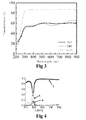
- Fig. 3 shows a graph of transmittance of measured samples 1 and 2 (including quartz substrates) and quartz substrates versus light wavelength;
- Fig. 5 shows the process of metal evaporation in fabrication with the microsphere photolithographic process and a SEM image of an electrode patterned into multiple parallel lines according to the first embodiment of the present invention
- Fig. 6 shows a graph of transmittance versus light wavelength, in case of having a substrate, when the patterned structure is crossing lines and the inter-line distance are 390, 400, 410 and 420 nm;
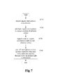
- Fig. 7 shows a flow chart of the method for fabricating the electrode according to the first embodiment of the present invention
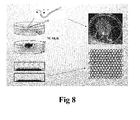
- Fig. 8 shows a mask fabricating process in NSL
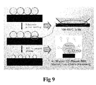
- Fig. 9 shows an RIE process of the mask in Fig. 8 ;
- Fig. 10 shows a diagram of a single-peak electrode according to the second embodiment of the present invention.
- Fig. 11 shows a graph of absorbance versus light frequency for the single-peak electrode in Fig. 10 when the strip lengths are 150nm, 160nm, 170nm and 180nm respectively;
- Fig. 12 shows a diagram of a three-peak electrode according to the second embodiment of the present invention.
- Fig. 13 shows a graph of absorbance versus light frequency for the 5-peak electrode according to the second embodiment of the present invention.
- Fig. 14 shows a flow chart of a method for fabricating the electrode according to the second embodiment of the present invention.
- the electrode according to the first embodiment of the present invention may include a substantially planar metallic thin film layer with a patterned structure, and the metallic thin film layer is configured to transmit an incident light through the metallic thin film layer.
- the metallic thin film layer has a patterned structure of an array of circular holes, and circular holes in the array are regularly distributed in the metallic thin film layer.
- circular holes in the array may be randomly distributed in the metallic thin film layer.
- the patterned structure may also be any one of the Escheric series of patterns.
- the patterned structure may include a plurality of parallel lines.
- the patterned structure may include a plurality of crossed lines.
- the parallel lines or crossed lines may be regularly distributed in the metallic thin film layer, or may also be randomly distributed in the metallic thin film layer.
- the planar metallic thin film layer with a patterned structure according to the first embodiment of the present invention may transmit a visible light, a near infrared light or an infrared light, and the transmittance may be 80%, 90%, 95% or higher.
- the metallic thin film layer in the electrode according to the first embodiment of the present invention may preferably have a surface roughness smaller than 1 ⁇ m, 100nm, 10nm or 1nm.
- materials for forming the metallic thin film layer may have a resistivity smaller than 0.005, 0.002 or 0.001 ⁇ •m
- a sheet resistance of the metallic thin film layer which is fabricated with the microsphere photolithographic process, with an array of circular holes as the patterned structure is given by the following equation: R sq ⁇ ⁇ d ⁇ 1 - r R - 1 wherein R sq is the sheet resistance of the metallic thin film layer, ⁇ is the resistivity of the material for forming the metallic thin film layer, d is the thickness of the metallic thin film layer, R is the microsphere radius prior to the microsphere lithography and r is the microsphere radius after sphere reduction process.
- the microspheres are made from polystyrene. Alternatively, the microspheres may be made from any other suitable organic substances or materials known in the art, such as silicon dioxide.
- d has a value range of 5 ⁇ 1000 nm
- R has a value range of 10nm ⁇ 10 ⁇ m
- the R sq of the electrode sample 200-1 may be obtained as 4.4 ⁇ / sq , and about 8 ⁇ / sq for R sq of the electrode sample 200-2, which agree well with the experimental results obtained by measuring electrode samples 200-1 and 200-2 formed as described above.
- optical characteristics of the electrode samples 200-1 and 200-2 fabricated as above may also be measured, and the obtained results are shown in Fig. 3 .
- the horizontal axis represents light wavelength
- the vertical axis represents transmittance.
- the gray line represents the graph of transmittance of the quartz substrate versus light wavelength
- the dotted line represents the graph of transmittance of electrode sample 200-1 versus light wavelength
- the black line represents the graph of the transmittance of electrode sample 200-2 versus light wavelength.
- Fig. 4 shows a graph of transmittance (T), absorbance (A) and reflectance (R) versus light wavelength of the electrode sample 400 with optimal structure according to the first embodiment of the present invention.
- the measured transmittance is almost 100%.
- a-Si:H dielectric constant
- the electrode's transmittance of T > 97% and sheet resistance R sq of about 8 ⁇ / sq in Fig. 4 the performance of the electrode in Fig. 4 is well above the performance of ITO.
- the patterned structure may include a plurality of parallel lines.
- the right part of Fig. 5 shows a SEM image of the electrode according to the first embodiment of the present invention fabricated with the microsphere photolithographic process, wherein the patterned structure in the electrode is a plurality of lines parallel with the selected direction, which may be an anisotropic system.
- the left part in Fig. 5 shows the process of metal evaporation at a grazing angle from 20 to 35 degree when fabricating the metallic thin film layer in which the patterned structure is a plurality of parallel lines.
- the patterned structure may also include a plurality of crossed lines.
- Fig. 6 shows a graph of transmittance versus light wavelength when the patterned structure is crossed lines (i.e. square holes) with a substrate and the inter-line distance is 390, 400, 410 and 420nm.
- the crossed lines are made from Ag with a film thickness of 40nm.
- corresponding sheet resistances are 9.3, 6.23, 4.68 and 3.74 ⁇ / sq , respectively.
- Fig. 7 shows a flow chart of a method for fabricating the electrode according to the first embodiment of the present invention.
- a substrate is, for example, a quartz substrate.
- the microspheres are made from polystyrene.
- other suitable materials known in the art such as silicon dioxide may be used.
- step S720 the microspheres are subjected to an etching back process such as a reactive ion etching (RIE) process to expose a part of a surface of the substrate.
- RIE reactive ion etching
- step S730 metal is deposited on the microspheres and the exposed surface of the substrate.
- step S740 the microspheres are peeled off to form a metallic thin film layer with a patterned structure, wherein the metallic thin film layer is configured to transmit an incident light through the metallic thin film layer.
- the patterned structure may be an array of circular holes, a plurality of parallel lines or a plurality of crossed lines.
- Fig. 8 and Fig. 9 show a processing procedure when the patterned structure is an array of circular holes, which may, for example, use a nanosphere lithography (NSL) technology.
- Fig. 8 shows processing steps in the NSL process. As shown in the left part of Fig. 8 , first of all, polystyrene microspheres are deposited on water surface, which then form a densely packed monolayer. After evaporating the water, an array of nanospheres deposits on a substrate. The deposited nanosphere array is then used as a mask for metal evaporation.
- the top diagram in the right part of Fig. 8 shows an optical image of the water surface with nanospheres floating on the water surface, and the bottom diagram shows the densely packed nanosphere array.
- the array pattern obtained as described above is that of isolated quasi-triangles, and thus non-conducting.
- Fig. 9 diameters of microspheres in the densely packed array are reduced by RIE. Thereafter, the array of microspheres with reduced diameters is used as a mask to evaporate metal. After completing metal evaporation, the microspheres are peeled off to form a metallic thin film layer with a patterned structure that is an array of circular holes.
- the processing procedure is substantially identical to that of an array of circular holes, and the only difference lies in that the metal evaporation process is carried out with grazing angles from 20 to 35 degree, as shown in the left part of Fig. 5 .
- the structure and fabricating method of the electrode according to the first embodiment of the present invention have been described as above.
- no transparent conductive oxide film or little transparent conductive oxide film may be used while fabricating the electrode, and piling process is not required, thereby preventing junctions quality from deteriorating due to the piled conductive oxide thick film.
- properly designing the size and structure of the patterned structure in the electrode according to the first embodiment of the present invention may ensure that the electrode have a high conductivity and a high transmittance.
- the planar electrode may be used as a window superstrate, allowing for a high quality planar PV junction to be deposited over it.
- Fig. 10 shows a structure diagram of a single-peak electrode 1000 according to the second embodiment of the present invention.
- the single-peak electrode 1000 is laminated on a light absorption layer 1010, which is laminated on an underlying metal film 1020, such as the metal back electrode.
- the single-peak electrode 1000 includes a planar metallic thin film layer pattern including a first micro-strip array with a first size and a first shape.
- the planar metallic thin film layer pattern is configured to transmit an incident light in a first wavelength range to the light absorption layer, wherein the first wavelength range is determined at least partly based on the first size and the first shape of the first micro-strip array.
- the micro-strip is of rectangle.
- the micro-strip may also take other proper shapes such as micro-strip holes or other forms of holes or islands.
- Fig. 11 shows a graph of absorbance and reflectance versus light frequency for the single-peak electrode in Fig. 10 when the strip lengths are 150nm, 160nm, 170nm and 180nm.
- the horizontal axis represents frequency in eV and the vertical axis represents the percentage.
- the broad absorption peak at 2.7eV is due to the intrinsic inter-band absorption of a-Si.
- the satellite peak e.g. the peak at 2.2eV for 180nm
- the relationship between its frequency (namely, wavelength) and strip length 1 follows the above equation (2).
- the absorption peak corresponds to an absorbance of about 70%, which is not ideal. However, the strip-to-strip distance may be reduced to improve the absorbance.
- the light absorption material layer may include a PN junction, a PIN junction or a plurality of junctions.
- the light absorption material includes a photovoltaic material.
- the light absorption material includes one of Si, CIGS, CIS, CdTe, GaAs, Cu 2 O, Zn 3 P 2 and SiC.
- the light absorption layer may also be a quantum dot layer.
- the light absorption layer may be a organic semiconductor film, such as PF10TBT:[C60] PCBM.
- the underlying metal film may not be patterned, or the underlying metal film may be patterned.
- planar metallic film layer has a surface roughness less than 1 ⁇ m, 100nm, 10nm or 1nm.
- the material for forming the planar metallic thin film layer has a resistivity less than 0.005, 0.002 or 0.001 ⁇ m .
- the electrode according to the second embodiment may be a multi-peak electrode.
- Fig. 12 shows the 3-peak electrode 1200 according to the second embodiment of the present invention, in which, in addition to the first micro-strip array 1201 with the first size and the first shape, the planar metallic thin film layer pattern 1200 may further include a second micro-strip array 1202 with a second size and a second shape and a third micro-strip array 1203 with a third size and a third shape, wherein the planar metallic thin film layer pattern is configured to not only transmit a light of the first wavelength range into the light absorption layer, but also transmit an incident light of a second and third wavelength range into the light absorption layer.
- the second wavelength range is determined at least partly based on the second size and the second shape of the second micro-strip array
- the third wavelength range is determined at least partly based on the third size and the third shape of the third micro-strip array.
- the 3-peak electrode 1200 is laminated on the light absorption layer 1210, and the light absorption layer 1210 is laminated on the underlying metal film 1220, such as the metallic back electrode.
- the electrode according to the second embodiment may be a 5-peak electrode.
- Fig. 13 shows a graph of absorbance versus light frequency of the 5-peak electrode according to the second embodiment of the present invention, which operates under an infrared light.
- the 5-peak electrode has 5 microstrip elements with different sizes such as lengths, and each peak corresponds to one microstrip element with a given length.
- low loss dielectric is used as the absorber for obtaining a very narrow absorption peak. Such light absorption may be realized in the visible light frequency range.
- Fig. 14 shows a flow chart of a method for fabricating the electrode according to the second embodiment of the present invention.
- a metal layer is deposited on a light absorption layer.
- a metallic layer is patterned to form a planar metallic thin film layer pattern at least including a first micro-strip array with a first size and a first shape, wherein the planar metallic film layer is configured to transmit an incident light in a first wavelength range into the light absorption layer, and wherein the first wavelength range is determined at least partly based on the first size and the first shape of the micro-strip array.
- electrodes according to embodiments of the present invention may be applicable not only to photovoltaic applications, i.e., solar cells, but also to optoelectronic applications, such as in LEDs.
Landscapes
- Photovoltaic Devices (AREA)
- Hybrid Cells (AREA)
Applications Claiming Priority (2)
| Application Number | Priority Date | Filing Date | Title |
|---|---|---|---|
| CN2010105249347A CN102082186B (zh) | 2010-10-29 | 2010-10-29 | 电极及其制造方法 |
| PCT/CN2011/079481 WO2012055302A1 (fr) | 2010-10-29 | 2011-09-08 | Electrode et son procédé de fabrication |
Publications (1)
| Publication Number | Publication Date |
|---|---|
| EP2634813A1 true EP2634813A1 (fr) | 2013-09-04 |
Family
ID=44088033
Family Applications (1)
| Application Number | Title | Priority Date | Filing Date |
|---|---|---|---|
| EP11833584.3A Withdrawn EP2634813A1 (fr) | 2010-10-29 | 2011-09-08 | Electrode et son procédé de fabrication |
Country Status (6)
| Country | Link |
|---|---|
| US (1) | US8698267B2 (fr) |
| EP (1) | EP2634813A1 (fr) |
| JP (1) | JP2013544024A (fr) |
| KR (1) | KR20140001729A (fr) |
| CN (1) | CN102082186B (fr) |
| WO (1) | WO2012055302A1 (fr) |
Cited By (1)
| Publication number | Priority date | Publication date | Assignee | Title |
|---|---|---|---|---|
| CN109553162A (zh) * | 2018-11-27 | 2019-04-02 | 昆明理工大学 | 一种以有序多孔ZnO为模板的不锈钢基纳米阵列β-PbO2电极的制备方法 |
Families Citing this family (11)
| Publication number | Priority date | Publication date | Assignee | Title |
|---|---|---|---|---|
| CN102082186B (zh) * | 2010-10-29 | 2013-05-08 | 华南师范大学 | 电极及其制造方法 |
| CN103474483B (zh) * | 2013-09-13 | 2017-10-17 | 南开大学 | 一种周期性结构的背反射电极及其制备方法 |
| KR101441607B1 (ko) * | 2014-02-13 | 2014-09-24 | 인천대학교 산학협력단 | 고효율 광전소자 및 그 제조방법 |
| CN104134736A (zh) * | 2014-07-28 | 2014-11-05 | 中国科学院半导体研究所 | 半导体器件、透明金属网状电极及其制作方法 |
| KR101602922B1 (ko) * | 2014-11-10 | 2016-03-14 | 한밭대학교 산학협력단 | 투명 컬러 태양전지 |
| CN105225728B (zh) * | 2015-09-29 | 2017-01-04 | 惠州易晖光电材料股份有限公司 | 一种低电阻透明导电薄膜及其制备方法 |
| CN106876261B (zh) * | 2015-12-10 | 2020-05-01 | 昆山工研院新型平板显示技术中心有限公司 | 一种柔性导电线,及其制备方法和应用 |
| CN105803500B (zh) * | 2016-04-05 | 2018-04-10 | 华南师范大学 | 一种花瓣状氧化亚铜及其制备方法和应用 |
| CN106082113A (zh) * | 2016-07-12 | 2016-11-09 | 中国科学院深圳先进技术研究院 | 一种利用微加工在电极表面制备三维微结构的方法 |
| KR101778723B1 (ko) * | 2016-11-17 | 2017-09-25 | 한국에너지기술연구원 | Cigs계 태양전지 셀의 제조방법 및 cigs계 태양전지 셀 |
| CN109545883B (zh) * | 2019-01-10 | 2023-12-26 | 中国科学院上海技术物理研究所 | 一种低暗电流台面型雪崩单光子探测器及制备方法 |
Family Cites Families (12)
| Publication number | Priority date | Publication date | Assignee | Title |
|---|---|---|---|---|
| US6441298B1 (en) * | 2000-08-15 | 2002-08-27 | Nec Research Institute, Inc | Surface-plasmon enhanced photovoltaic device |
| US7373034B2 (en) * | 2004-09-02 | 2008-05-13 | Nec Corporation | Optoelectronic hybrid integrated module |
| US7466269B2 (en) * | 2006-05-24 | 2008-12-16 | Wavebender, Inc. | Variable dielectric constant-based antenna and array |
| JP5571870B2 (ja) | 2007-09-21 | 2014-08-13 | 株式会社東芝 | 極微細構造を有する光透過型金属電極およびその製造方法 |
| US20100175749A1 (en) * | 2008-03-24 | 2010-07-15 | Tsutsumi Eishi | Solar cell and method for manufacturing metal electrode layer to be used in the solar cell |
| EP2109147A1 (fr) * | 2008-04-08 | 2009-10-14 | FOM Institute for Atomic and Molueculair Physics | Cellule photovoltaïque avec nano-structures à génération de résonance à plasmons de surface |
| CN101323504A (zh) * | 2008-06-13 | 2008-12-17 | 天津大学 | 大孔-介孔纳米晶二氧化钛薄膜的制备方法 |
| US8298852B2 (en) * | 2008-12-29 | 2012-10-30 | Jusung Engineering Co., Ltd. | Thin film type solar cell and method for manufacturing the same |
| JP2010219407A (ja) * | 2009-03-18 | 2010-09-30 | Toshiba Corp | メッシュ構造を有する電極を具備した太陽電池及びその製造方法 |
| JP5667748B2 (ja) * | 2009-03-18 | 2015-02-12 | 株式会社東芝 | 光透過型太陽電池およびその製造方法 |
| CN101807613B (zh) * | 2010-03-29 | 2011-05-25 | 哈尔滨工业大学 | 三维光子晶体为背反射层的非晶硅太阳电池及其制备方法 |
| CN102082186B (zh) * | 2010-10-29 | 2013-05-08 | 华南师范大学 | 电极及其制造方法 |
-
2010
- 2010-10-29 CN CN2010105249347A patent/CN102082186B/zh not_active Expired - Fee Related
-
2011
- 2011-09-08 KR KR1020127010957A patent/KR20140001729A/ko not_active Withdrawn
- 2011-09-08 EP EP11833584.3A patent/EP2634813A1/fr not_active Withdrawn
- 2011-09-08 WO PCT/CN2011/079481 patent/WO2012055302A1/fr not_active Ceased
- 2011-09-08 US US13/503,903 patent/US8698267B2/en not_active Expired - Fee Related
- 2011-09-08 JP JP2013535251A patent/JP2013544024A/ja active Pending
Non-Patent Citations (1)
| Title |
|---|
| See references of WO2012055302A1 * |
Cited By (2)
| Publication number | Priority date | Publication date | Assignee | Title |
|---|---|---|---|---|
| CN109553162A (zh) * | 2018-11-27 | 2019-04-02 | 昆明理工大学 | 一种以有序多孔ZnO为模板的不锈钢基纳米阵列β-PbO2电极的制备方法 |
| CN109553162B (zh) * | 2018-11-27 | 2021-08-20 | 昆明理工大学 | 一种以有序多孔ZnO为模板的不锈钢基纳米阵列β-PbO2电极的制备方法 |
Also Published As
| Publication number | Publication date |
|---|---|
| US8698267B2 (en) | 2014-04-15 |
| JP2013544024A (ja) | 2013-12-09 |
| KR20140001729A (ko) | 2014-01-07 |
| CN102082186A (zh) | 2011-06-01 |
| WO2012055302A1 (fr) | 2012-05-03 |
| CN102082186B (zh) | 2013-05-08 |
| US20120273915A1 (en) | 2012-11-01 |
Similar Documents
| Publication | Publication Date | Title |
|---|---|---|
| US8698267B2 (en) | Electrode and fabricating method thereof | |
| KR101008274B1 (ko) | 적층형 광전 변환 장치 | |
| US7847180B2 (en) | Nanostructure and photovoltaic cell implementing same | |
| KR101247916B1 (ko) | 텐덤 반도체 층 스택을 구비한 광전지 모듈 및 광전지 모듈의 제작 방법 | |
| EP4531113B1 (fr) | Cellule solaire et module photovoltaïque | |
| EP1100130A1 (fr) | Dispositif photoelectrique a couches minces et a base de silicium | |
| CN101562207A (zh) | 晶体硅太阳能电池 | |
| Pudasaini et al. | Aluminum oxide passivated radial junction sub-micrometre pillar array textured silicon solar cells | |
| Yin et al. | Rear point contact structures for performance enhancement of semi-transparent ultrathin Cu (In, Ga) Se2 solar cells | |
| CN103872153B (zh) | 一种以金属微纳结构作为中间电极的级联太阳能电池 | |
| CN216624297U (zh) | 异质结太阳能电池和光伏组件 | |
| Hsueh et al. | Crystalline-Si photovoltaic devices with ZnO nanowires | |
| KR101194243B1 (ko) | 탠덤형 광기전력 장치 및 이의 제조 방법 | |
| US20100212721A1 (en) | Thin film type solar cell and method for manufacturing the same | |
| US20110011448A1 (en) | Thin film solar cell and method of manufacturing the same | |
| US20140209154A1 (en) | Embedded Nanopatterns for Optical Absorbance and Photovoltaics | |
| Yamamoto | Thin-film crystalline silicon solar cells | |
| Massiot | Design and fabrication of nanostructures for light-trapping in ultra-thin solar cells | |
| Terukov et al. | Investigation of the characteristics of heterojunction solar cells based on thin single-crystal silicon wafers | |
| Jia et al. | Conductive white back reflector and scatter based on ZnO nanostructure arrays for harvesting solar energy | |
| US20230402558A1 (en) | Hot carrier solar cell and tandem solar cell | |
| JP2003142705A (ja) | 光起電力素子 | |
| HK1155275A (en) | Super-electrode and the manufacturing method thereof | |
| Yin | Nanocomposite thin films for solar energy conversion | |
| CN117855293A (zh) | 太阳能电池及其制备方法和光伏组件 |
Legal Events
| Date | Code | Title | Description |
|---|---|---|---|
| PUAI | Public reference made under article 153(3) epc to a published international application that has entered the european phase |
Free format text: ORIGINAL CODE: 0009012 |
|
| 17P | Request for examination filed |
Effective date: 20120426 |
|
| AK | Designated contracting states |
Kind code of ref document: A1 Designated state(s): AL AT BE BG CH CY CZ DE DK EE ES FI FR GB GR HR HU IE IS IT LI LT LU LV MC MK MT NL NO PL PT RO RS SE SI SK SM TR |
|
| DAX | Request for extension of the european patent (deleted) | ||
| STAA | Information on the status of an ep patent application or granted ep patent |
Free format text: STATUS: THE APPLICATION IS DEEMED TO BE WITHDRAWN |
|
| 18D | Application deemed to be withdrawn |
Effective date: 20160401 |