EP2634823B1 - Led-beleuchtungsschaltung, led-beleuchtungsvorrichtung und buchse für eine led-beleuchtungseinheit - Google Patents
Led-beleuchtungsschaltung, led-beleuchtungsvorrichtung und buchse für eine led-beleuchtungseinheit Download PDFInfo
- Publication number
- EP2634823B1 EP2634823B1 EP11836498.3A EP11836498A EP2634823B1 EP 2634823 B1 EP2634823 B1 EP 2634823B1 EP 11836498 A EP11836498 A EP 11836498A EP 2634823 B1 EP2634823 B1 EP 2634823B1
- Authority
- EP
- European Patent Office
- Prior art keywords
- led
- circuit
- capacitor
- terminal voltage
- control unit
- Prior art date
- Legal status (The legal status is an assumption and is not a legal conclusion. Google has not performed a legal analysis and makes no representation as to the accuracy of the status listed.)
- Not-in-force
Links
- 239000003990 capacitor Substances 0.000 claims description 101
- 238000005286 illumination Methods 0.000 claims description 69
- 230000010355 oscillation Effects 0.000 claims description 41
- 230000000903 blocking effect Effects 0.000 claims description 20
- 229910052715 tantalum Inorganic materials 0.000 claims description 11
- GUVRBAGPIYLISA-UHFFFAOYSA-N tantalum atom Chemical group [Ta] GUVRBAGPIYLISA-UHFFFAOYSA-N 0.000 claims description 10
- 238000010586 diagram Methods 0.000 description 23
- 229910052736 halogen Inorganic materials 0.000 description 15
- 150000002367 halogens Chemical class 0.000 description 15
- 239000003985 ceramic capacitor Substances 0.000 description 13
- 238000013016 damping Methods 0.000 description 5
- 230000000694 effects Effects 0.000 description 4
- 238000009499 grossing Methods 0.000 description 4
- 239000000758 substrate Substances 0.000 description 4
- 230000015556 catabolic process Effects 0.000 description 3
- 230000017525 heat dissipation Effects 0.000 description 2
- 230000001629 suppression Effects 0.000 description 2
- 238000006243 chemical reaction Methods 0.000 description 1
- 238000010276 construction Methods 0.000 description 1
- 230000007423 decrease Effects 0.000 description 1
- 230000007812 deficiency Effects 0.000 description 1
- 238000006731 degradation reaction Methods 0.000 description 1
- 230000001419 dependent effect Effects 0.000 description 1
- 239000003792 electrolyte Substances 0.000 description 1
- 238000005516 engineering process Methods 0.000 description 1
- 230000002708 enhancing effect Effects 0.000 description 1
- 230000020169 heat generation Effects 0.000 description 1
- 238000010438 heat treatment Methods 0.000 description 1
- 230000001939 inductive effect Effects 0.000 description 1
- 230000000977 initiatory effect Effects 0.000 description 1
- 230000007257 malfunction Effects 0.000 description 1
- 238000012544 monitoring process Methods 0.000 description 1
- 230000002093 peripheral effect Effects 0.000 description 1
- 230000000630 rising effect Effects 0.000 description 1
- 239000004065 semiconductor Substances 0.000 description 1
- 239000013589 supplement Substances 0.000 description 1
- 150000003481 tantalum Chemical class 0.000 description 1
Images





Classifications
-
- H—ELECTRICITY
- H02—GENERATION; CONVERSION OR DISTRIBUTION OF ELECTRIC POWER
- H02M—APPARATUS FOR CONVERSION BETWEEN AC AND AC, BETWEEN AC AND DC, OR BETWEEN DC AND DC, AND FOR USE WITH MAINS OR SIMILAR POWER SUPPLY SYSTEMS; CONVERSION OF DC OR AC INPUT POWER INTO SURGE OUTPUT POWER; CONTROL OR REGULATION THEREOF
- H02M1/00—Details of apparatus for conversion
- H02M1/32—Means for protecting converters other than automatic disconnection
-
- H—ELECTRICITY
- H02—GENERATION; CONVERSION OR DISTRIBUTION OF ELECTRIC POWER
- H02M—APPARATUS FOR CONVERSION BETWEEN AC AND AC, BETWEEN AC AND DC, OR BETWEEN DC AND DC, AND FOR USE WITH MAINS OR SIMILAR POWER SUPPLY SYSTEMS; CONVERSION OF DC OR AC INPUT POWER INTO SURGE OUTPUT POWER; CONTROL OR REGULATION THEREOF
- H02M7/00—Conversion of AC power input into DC power output; Conversion of DC power input into AC power output
- H02M7/02—Conversion of AC power input into DC power output without possibility of reversal
- H02M7/04—Conversion of AC power input into DC power output without possibility of reversal by static converters
- H02M7/06—Conversion of AC power input into DC power output without possibility of reversal by static converters using discharge tubes without control electrode or semiconductor devices without control electrode
-
- H—ELECTRICITY
- H02—GENERATION; CONVERSION OR DISTRIBUTION OF ELECTRIC POWER
- H02M—APPARATUS FOR CONVERSION BETWEEN AC AND AC, BETWEEN AC AND DC, OR BETWEEN DC AND DC, AND FOR USE WITH MAINS OR SIMILAR POWER SUPPLY SYSTEMS; CONVERSION OF DC OR AC INPUT POWER INTO SURGE OUTPUT POWER; CONTROL OR REGULATION THEREOF
- H02M7/00—Conversion of AC power input into DC power output; Conversion of DC power input into AC power output
- H02M7/42—Conversion of DC power input into AC power output without possibility of reversal
- H02M7/44—Conversion of DC power input into AC power output without possibility of reversal by static converters
- H02M7/48—Conversion of DC power input into AC power output without possibility of reversal by static converters using discharge tubes with control electrode or semiconductor devices with control electrode
- H02M7/53—Conversion of DC power input into AC power output without possibility of reversal by static converters using discharge tubes with control electrode or semiconductor devices with control electrode using devices of a triode or transistor type requiring continuous application of a control signal
- H02M7/537—Conversion of DC power input into AC power output without possibility of reversal by static converters using discharge tubes with control electrode or semiconductor devices with control electrode using devices of a triode or transistor type requiring continuous application of a control signal using semiconductor devices only, e.g. single switched pulse inverters
- H02M7/5383—Conversion of DC power input into AC power output without possibility of reversal by static converters using discharge tubes with control electrode or semiconductor devices with control electrode using devices of a triode or transistor type requiring continuous application of a control signal using semiconductor devices only, e.g. single switched pulse inverters in a self-oscillating arrangement
-
- H—ELECTRICITY
- H05—ELECTRIC TECHNIQUES NOT OTHERWISE PROVIDED FOR
- H05B—ELECTRIC HEATING; ELECTRIC LIGHT SOURCES NOT OTHERWISE PROVIDED FOR; CIRCUIT ARRANGEMENTS FOR ELECTRIC LIGHT SOURCES, IN GENERAL
- H05B45/00—Circuit arrangements for operating light-emitting diodes [LED]
- H05B45/30—Driver circuits
- H05B45/37—Converter circuits
-
- F—MECHANICAL ENGINEERING; LIGHTING; HEATING; WEAPONS; BLASTING
- F21—LIGHTING
- F21K—NON-ELECTRIC LIGHT SOURCES USING LUMINESCENCE; LIGHT SOURCES USING ELECTROCHEMILUMINESCENCE; LIGHT SOURCES USING CHARGES OF COMBUSTIBLE MATERIAL; LIGHT SOURCES USING SEMICONDUCTOR DEVICES AS LIGHT-GENERATING ELEMENTS; LIGHT SOURCES NOT OTHERWISE PROVIDED FOR
- F21K9/00—Light sources using semiconductor devices as light-generating elements, e.g. using light-emitting diodes [LED] or lasers
- F21K9/20—Light sources comprising attachment means
- F21K9/23—Retrofit light sources for lighting devices with a single fitting for each light source, e.g. for substitution of incandescent lamps with bayonet or threaded fittings
-
- F—MECHANICAL ENGINEERING; LIGHTING; HEATING; WEAPONS; BLASTING
- F21—LIGHTING
- F21Y—INDEXING SCHEME ASSOCIATED WITH SUBCLASSES F21K, F21L, F21S and F21V, RELATING TO THE FORM OR THE KIND OF THE LIGHT SOURCES OR OF THE COLOUR OF THE LIGHT EMITTED
- F21Y2115/00—Light-generating elements of semiconductor light sources
- F21Y2115/10—Light-emitting diodes [LED]
-
- Y—GENERAL TAGGING OF NEW TECHNOLOGICAL DEVELOPMENTS; GENERAL TAGGING OF CROSS-SECTIONAL TECHNOLOGIES SPANNING OVER SEVERAL SECTIONS OF THE IPC; TECHNICAL SUBJECTS COVERED BY FORMER USPC CROSS-REFERENCE ART COLLECTIONS [XRACs] AND DIGESTS
- Y02—TECHNOLOGIES OR APPLICATIONS FOR MITIGATION OR ADAPTATION AGAINST CLIMATE CHANGE
- Y02B—CLIMATE CHANGE MITIGATION TECHNOLOGIES RELATED TO BUILDINGS, e.g. HOUSING, HOUSE APPLIANCES OR RELATED END-USER APPLICATIONS
- Y02B20/00—Energy efficient lighting technologies, e.g. halogen lamps or gas discharge lamps
- Y02B20/30—Semiconductor lamps, e.g. solid state lamps [SSL] light emitting diodes [LED] or organic LED [OLED]
Definitions
- the present invention relates to an LED lighting circuit that can properly light an LED even with a power supply obtained from an inverter circuit, and also relates to an LED illumination device and an LED illumination unit socket.
- Halogen lamps that operate at a rated voltage of 12 V are in widespread use.
- the power supply for such halogen lamps is often produced by stepping down a line supply voltage.
- a conventional step-down transformer is bulky, a device (hereinafter referred to as an electronic transformer) is employed that converts the AC line supply voltage to a high-frequency voltage by using an inverter circuit and then converts the voltage to a lower voltage by using a high-frequency transformer.
- the inverter circuit to be used in the electronic transformer is one of two types, a self-excited oscillation type or an externally excited oscillation type, refer, for example, to Figure 6 in laid-open publication JP H02-66890 A (patent document 1).
- FIG. 12 is a diagram showing a lighting device equipped with a self-excited inverter as presented in the description of the prior art in patent document 1.
- the lighting device comprises an AC power supply 1, a full-wave rectifier 2, a halogen lamp 14, a half-bridge inverter circuit, and other circuit elements, and the entire circuitry, excluding the AC power supply 1 and the halogen lamp 14, corresponds to the electronic transformer.
- a circuit comprising a resistor 5, a capacitor 6, and a triggering device 7 outputs an oscillation initiating trigger when a predetermined voltage is reached.
- Self-excited oscillation occurs within a circuit comprising capacitors 3 and 4, transistors 8 and 9, and a current feedback transformer 13.
- a high-frequency step-down transformer 12 produces an AC drive voltage for the halogen lamp 14.
- Diodes 10 and 11 are protection diodes for providing protection against back electromotive force.
- the lighting device depicted in Figure 12 shows the operating principle of the half-bridge inverter circuit.
- patent document 1 The invention disclosed in patent document 1 is intended to suppress the rush current that occurs during startup, and for that purpose, a soft start circuit A and a voltage feedback circuit B are provided as shown in Figure 1 included in patent document 1.
- LED illumination devices have begun to be used widely, replacing not only incandescent lamps but also halogen lamps.
- Conventional halogen lamps have power ratings of 20 to 40 W but, in the case of LED illumination devices, brightness comparable to halogen lamps can be obtained at 4W which is about one-fifths of the above power rating.
- the self-excited electronic transformer is inserted between the AC line power supply and the halogen lamp bayonet base (MR16 or MR11 in the case of 12-V halogen lamps), as described above, the LED illumination device may not light (or may turn on and off erratically).
- Electronic transformers widely used for halogen lamps range from small ones for driving single halogen lamps to large ones rated for 100 to 300 W capable of driving several halogen lamps.
- the minimum operating power necessary for startup is specified in order to produce a stable output of 12 VAC, and generally a circuit load of 10 to 30 W is required.
- the output of the electronic transformer may become unstable due to an insufficient load, causing the LED illumination device to malfunction by failing to light or turning on and off erratically.
- Figure 13 is a diagram redrawn from Figure 2 from patent document 2.
- the output of a self-excited electronic transformer inverter-type voltage conversion circuit
- a lighting circuit 40 first supplies current to a startup assisting circuit 42, inducing self-excited oscillation in the electronic transformer.
- a constant-current load circuit 43 draws a constant current from the electronic transformer to stabilize the oscillation.
- the lighting circuit 40 causes the LED 22 to light, while at the same time, stopping the operation of the constant-current load circuit 43.
- the constant-current load circuit 43 supplements the power consumed by the LED 22 and thereby provides the power necessary for the electronic transformer to continue to operate. That is, since the power for driving the constant-current load circuit 43 becomes necessary in addition to the power necessary for driving the LED 22 itself, a large amount of power is required as a whole, thus partially defeating the purpose of the LED illumination device that features low-power operation. Furthermore, when a halogen lamp having a small external size is replaced by an LED illumination device, there arises a need to take account of not only the limitation on the heat dissipation capability of the LED illumination device itself but also the heat dissipation of the constant-current load circuit. In this case, heat generation has to be reduced by reducing the power of the LED.
- Laid-open publication US 2009/0122580 A1 discloses a thyristor power control circuit configured to prevent electromagnetic interference (EMI) and to this end comprises a thyristor, a rectifier, a power converter, and a damping circuit, where this thyristor power control circuit may be used in a power supply circuit for an LED lighting device.
- the damping circuit may be formed by an RC network connected in parallel to an output terminal of the rectifier so as to eliminate ringing current and to maintain a necessary holding current in the thyristor during a ON period of the thyristor for preventing flickering of the LED device.
- a diode may be coupled in parallel to the resistor of the damping RC network to prevent power loss at the damping resistor when the capacitor of the RC network is discharged.
- the invention achieves these and other objects by providing an LED lighting circuit having the features of claim 1, an LED illumination device having the features of claim 9, and an LED illumination unit socket having the features of claim 10.
- Advantageous embodiments of the invention are mentioned in the dependent claims.
- the terminal voltage control unit is a parallel circuit which includes a capacitor and a resistor.
- the capacitor in the terminal voltage control unit is a tantalum capacitor or an electrolytic capacitor.
- the terminal voltage control unit includes a second resistor which is connected in series with the capacitor.
- the terminal voltage control unit includes a Zener diode which is connected in parallel with the capacitor.
- the terminal voltage control unit includes a second capacitor which is connected in parallel with the capacitor and the second resistor.
- the capacitor is discharged with a time constant that is set longer than two cycles of the AC output of the AC power supply.
- the reverse current blocking unit comprises at least one diode.
- An LED illumination unit socket with which is connected an LED illumination unit having an LED driving unit for driving an LED includes a rectifier circuit which takes as input an AC output from an AC power supply, and which supplies a rectified output to the LED driving unit, a reverse current blocking unit provided between the rectifier circuit and the LED driving unit; and a terminal voltage control unit which operates to reduce an output terminal voltage of the rectifier circuit when the AC output from the AC power supply becomes unstable or stops.
- the problem that the LED does not light or turns on and off erratically can be avoided, regardless of whether the electronic transformer for the AC power supply is of a self-excited oscillation type or an externally excited oscillation type.
- the present inventor has discovered that when the electronic transformer stops due to an insufficient load, if the output terminal voltage of the rectifier circuit is reduced, the electronic transformer resumes oscillation.
- the present invention has been devised by utilizing this phenomenon.
- the terminal voltage control unit Upon detecting that the output of the AC power supply has stopped (or has become unstable), the terminal voltage control unit operates to reduce the output terminal voltage of the rectifier circuit.
- the reverse current blocking unit acts to block the current flowing from the LED driving unit back to the output terminal side of the rectifier circuit.
- the reverse current blocking unit electrically isolates the LED driving unit from the terminal voltage control unit; as a result, the voltage at the output terminal side of the rectifier circuit quickly drops, and thus the electronic transformer quickly resumes oscillation.
- the LED lighting circuit, the LED illumination device, and the apparatus constructed by connecting the LED illumination unit with the LED illumination unit socket are allowed to continue to operate in a stable manner.
- the provision of the terminal voltage control unit in conjunction with the revere current blocking unit serves to reduce the number of circuit components and minimize the power not relevant to lighting.
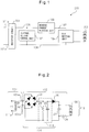
- Figure 1 is a schematic block diagram showing the configuration of an LED lighting circuit 100.
- the LED lighting circuit 100 comprises a rectifier circuit 101, a terminal voltage control unit 102, a reverse current blocking unit 103, and an LED driving unit 104.
- three LEDs 105 are shown as being connected to the LED lighting circuit 100.
- the rectifier circuit 101 has terminals 101a and 101b at which power is supplied from an AC power supply, and thus the output of the AC power supply is supplied as input to the rectifier circuit 101.
- the output of the rectifier circuit 101 is coupled via a wiring line 106 to both the terminal voltage control unit 102 and the reverse current blocking unit 103.
- the output of the reverse current blocking unit 103 is coupled via a wiring line 107 to the LED driving unit 104.
- the LED driving unit 104 drives the three LEDs 105 connected in series. Current from the terminal voltage control unit 102 and the LED driving unit 104 is returned to the rectifier circuit 101 via a wiring line 108.
- the terminal voltage control unit 102 operates to reduce the output terminal voltage of the rectifier circuit 101 (the voltage on the wiring line 106).
- the reverse current blocking unit 103 acts to block the current flowing from the LED driving unit 104 back to the output terminal side of the rectifier circuit 101.
- FIG. 2 is a detailed circuit diagram showing a circuit incorporating the LED lighting circuit 100 of Figure 1 .
- the secondary side n2 of a high-frequency step-down transformer 111a in the AC power supply 111 is connected to the terminals 101a and 101b.
- the primary side n1 is inserted in a path through which flows a high-frequency alternating current output from an inverter circuit contained in the AC power supply 111.
- the LED lighting circuit 100 in Figure 1 corresponds to the portion 112 shown in Figure 2 .
- the rectifier circuit 101 in Figure 1 is constructed from a diode bridge circuit comprising four diodes 23.
- the terminal voltage control unit 102 in Figure 1 is constructed from a parallel circuit 115 comprising a resistor 24 and a capacitor 25.
- the reverse current blocking unit 103 in Figure 1 is constructed from a diode 26.
- the LED driving unit 104 in Figure 1 is constructed from a combination of a capacitor 27 and a resistor 28.
- the LED lighting circuit 100 includes the terminals 101a and 101b, and the secondary side n2 of the high-frequency step-down transformer 111a is connected to the diode bridge circuit via the terminals 101a and 101b.
- the current output terminal of the diode bridge circuit is connected to the positive terminal of the resistor 24, the positive terminal of the capacitor 25, and the anode of the diode 26.
- the cathode of the diode 26 and the positive terminal of the capacitor 27 are together connected to the positive terminal of the LED array 113 constructed from the three LEDs 105 connected in series.
- the negative terminal of the LED array 113 is connected to the current limiting resistor 28.
- the negative terminals of the resistor 24, capacitors 25 and 27, and resistor 28, respectively, are connected to a wiring line through which current is returned via the diode bridge circuit to the AC power supply 111 (the secondary side n2 of the high-frequency step-down transformer 111a.)
- the capacitor 27 in the LED driving unit 104 is a smoothing capacitor for smoothing the current to be supplied to the LED array 113, while the resistor 28 is a current limiting resistor for limiting the current flowing to the LED array 113.
- That the output of the AC power supply becomes unstable means that the oscillation of the inverter in the AC power supply becomes weaker and the amplitude of the AC power supply output decreases (for example, to 50% or less of the normal amplitude level) or that such a situation is beginning to occur.
- the rectifier circuit 101 is not limited to the diode bridge configuration, but may be constructed from a single diode.
- the terminal voltage control unit 102 may be constructed from a circuit comprising a switching device such as an FET or a bipolar transistor, since it is only required to reduce the output terminal voltage of the rectifier circuit 101. In that case, the oscillating state of the AC power supply 111 is monitored, and the switching device is turned on based on the monitoring information. For example, when the output of the AC power supply is unstable or stops, the terminal voltage control unit 102 operates to reduce the output terminal voltage of the rectifier circuit 101 to about 5 to 7 V. This helps to restore the oscillation of the inverter in the AC power supply 111.
- a switching device such as an FET or a bipolar transistor
- the reverse current blocking unit 103 is not limited to a diode, but instead, use may be made of a switching device. In that case, the oscillating state of the AC power supply 111 or the result of a comparison made between the magnitude of the drive voltage of the LED driving unit 104 and the magnitude of the output terminal voltage of the rectifier circuit 101 is monitored to control the on/off operation of the switching device.
- the LED driving unit 104 may be constructed using a known voltage step-up circuit, voltage step-down circuit, or constant-current circuit.
- the resistor 28 may be replaced by a known constant-current circuit. If stray capacitance can be used, the capacitor 25 may be omitted.
- the value of the resistor 24 is 160 ⁇
- the value of the capacitor 25 is 10 ⁇ F
- the value of the capacitor 27 is 220 ⁇ F, though these values may vary depending on the rating of the electronic transformer and the current consumption of the LED array.
- the time constant of the parallel circuit of the resistor 24 and capacitor 25 is 1.6 ms; since the oscillation frequency of the inverter is about 30 kHz to 80 kHz, it follows that the time constant is several to several tens of times as long as the oscillation period. If the time constant is at least about twice the oscillation period, erroneous oscillation of the inverter contained in the electronic transformer can be prevented. Further, since the power supply is a 12-V power supply, three LEDs 105, each with a forward voltage of about 3 V, are connected in series.
- Figure 3 is a diagram showing voltage waveforms taken at various parts in the circuit of Figure 2 .
- Figure 3(a) shows one cycle of the AC waveform of the AC line power supply in order to provide a general idea of the time relationship.
- Figure 3(b) shows the voltage waveform taken at the cathode of the diode 26. That is, Figure 3(b) shows the drive voltage of the LED driving unit 104, which is also the voltage applied to the positive side of the LED array 3.
- This voltage waveform rises with a short delay relative to the rising of the AC line power supply, has a peak near the peak of the AC line power supply, and thereafter gradually falls.
- the voltage (in absolute value) of the AC line power supply rises above a certain level, the oscillation of the inverter circuit contained in the electronic transformer continues to persist, as will be described later, and extra power is available to charge the capacitor 27, as a result of which the voltage waveform shown in Figure 3(b) rises.
- Figure 3(c) shows a voltage waveform applied to the terminal 101a.
- Each pentagonal portion corresponds to the period during which the oscillation output is produced.
- the period defined by the parallel top and bottom sides represents the full oscillation period
- the period defined by the sloping sides represents the decay period. That is, in the lighting circuit shown in Figure 2 , the oscillation of the electronic transformer rises rapidly, and decays after a certain period of oscillation.
- Figure 3(c) also shows that the oscillation period is short when the AC line supply voltage is low, and long when the AC line supply voltage is high.
- Figure 3(c) further shows that when the AC line supply voltage exceeds a given value (in absolute value), the inverter circuit begins to oscillate, and also that the oscillation is intermittent.
- Figure 3(d) shows, in enlarged form, the periods corresponding to two pentagonal portions in Figure 3(c) .
- One oscillation period corresponding to one pentagonal portion in Figure 3(c) is shown as containing AC pulses for four cycles, but actually, it contains ten to several tens of AC pulses.
- the AC pulses are distorted and generally appear as a square wave.
- the frequency is about 30 to 80 kHz, as earlier noted.
- the oscillation is shown as decaying in two cycles, but it decays relatively quickly in a few cycles. That is, the oscillation of the inverter circuit continues for a certain period, and then decays and stops.
- the terminal voltage control unit 102 reduces the output voltage of the diode bridge circuit by detecting the above situation, the inverter circuit resumes oscillation. This operation is repeated.
- Figure 3(e) shows the voltage waveform taken at the output terminal of the diode bridge circuit.
- the voltage rises to its maximum value almost simultaneously with the start of the oscillation, and the maximum voltage is maintained during the oscillation period; then, when the oscillation ends, the voltage decays. Actually, some ripple occurs during the oscillation period, but such ripple is not shown here.
- the inverter circuit resumes oscillation, and the above operation is repeated.
- the waveform is closely observed, it is seen that the oscillation resumes when the output terminal voltage drops to a given fraction of the maximum voltage maintained during the oscillation period.
- Figure 4 is a cross-sectional view schematically illustrating a cross section of an LED illumination device 140.
- Two pins 144 protruding from the bottom of the outer casing 141 of the LED illumination device 140 correspond to the terminals 101a and 101b in Figure 2 and are connected to a lighting circuit block 143.
- the LED lighting circuit 112 shown in Figure 2 is contained in the lighting circuit block 143.
- Three LEDs 105 are mounted on a substrate 142 disposed above the lighting circuit block 143.
- the lighting circuit 143 is connected to the substrate 142 via interconnecting lines 145.
- the sloping face in the upper part of the outer casing 141 is formed in the shape of a reflecting mirror.
- the LED illumination device 140 shown here is compatible with a pin socket (MR16 bayonet base), but the first and second terminals 101a and 101b may be designed so as to be compatible with a screw-in socket.
- Figure 5 is a diagram showing a construction in which an LED illumination unit 150 and an LED illumination unit socket 160 are separated from each other.
- Figure 5(a) is a cross-sectional view schematically illustrating the LED illumination unit 150
- Figure 5(b) is a cross-sectional view schematically illustrating the LED illumination unit socket 160.
- the difference between the LED illumination device 140 shown in Figure 4 and the LED illumination unit 150 to be fitted into the LED illumination unit socket 160 shown in Figure 5 is that the lighting circuit block 143 of the LED illumination device 140 is replaced by an LED driving unit 153 in the LED illumination unit 150.
- the LED driving unit 153 corresponds to the LED driving unit 104 in Figure 1 , and may be constructed from a smoothing circuit or a constant-current circuit or the like.
- a substrate 152 on which three LEDs 105 are mounted is connected via interconnecting lines 155 to the LED driving unit 153 to which pins 154 are also connected. Since the LED illumination unit socket 160 outputs DC, as will be described later, the pins 154 connected to the LED driving unit 153 have polarities.
- Recesses 161 to accommodate the pins 154 for electrical connections are formed in the upper part of a mold 162 of the LED illumination unit socket 160 shown in Figure 5(b) .
- the electrodes of the recesses 161 are connected to a lighting circuit block 163 via interconnecting lines 165.
- the rectifier circuit 101, terminal voltage control circuit 102, and reverse current blocking circuit 103 shown in Figure 1 are contained in the lighting circuit block 163.
- the lighting circuit block 163 corresponds to a portion shown as an LED illumination device socket circuit 114 in Figure 2 . Accordingly, when the LED illumination unit 150 is connected to the LED illumination unit socket 160, the configuration is the same as that shown in Figure 1 and thus the entire circuit operates properly when connected to an electronic transformer.
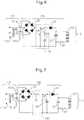
- Figure 6 is a detailed circuit diagram showing a circuit incorporating an alternative LED lighting circuit 170.
- the capacitor 25 may oscillate and generate noise through the mounting substrate. It is believed that the noise is associated with the intermittent operation of the electronic transformer.
- the resistor 67 By connecting the resistor 67 in series of the capacitor 68 as shown in the LED lighting circuit 170, it becomes possible to reduce the noise that may be generated when the capacitor 68 is formed from a ceramic capacitor. It is believed that the resistor 67 serves to smooth changes in the voltage developed across the terminals of the capacitor 68 and thus contributes to reducing the noise. However, the resistance value of the resistor 67 must be held to a minimum necessary value in order to not interfere with the induced oscillation of the electronic transformer.
- the noise from the capacitor 68 can be further reduced. This is presumably because the electrode structure of a tantalum capacitor or electrolytic capacitor is not a rigid structure such as that of a ceramic capacitor and the noise (chatter) is suppressed due to the damping of an electrolyte contained in the tantalum capacitor or electrolytic capacitor. That is, by not only inserting the resistor 67 but also using a tantalum capacitor or electrolytic capacitor as the capacitor 68, the effect of suppressing the noise can be further enhanced.
- the circuit shown in Figure 6 can be incorporated in the LED illumination device shown in Figure 4 .
- the circuit shown in Figure 6 can also be incorporated in the illumination device/socket combination shown in Figure 5 .
- Figure 7 is a detailed circuit diagram showing a circuit incorporating another alternative LED lighting circuit 180.
- the resistor 72 is connected in series with the resistor 24, the capacitor 25, and the diode 26 (series-parallel connection). By inserting the resistor 72, the noise from the capacitor 25 can be reduced when a ceramic capacitor is used as the capacitor 25.
- the resistor 72 serves to smooth changes in the voltage developed across the terminals of the capacitor 25 and thus contributes to reducing the noise. Further, the resistor 72 can be made smaller in value than the resistor 24, and if a fusible resistor is used as the resistor 72, the circuit safety can be further increased. By not only inserting the resistor 72 but also using a tantalum capacitor or electrolytic capacitor as the capacitor 25, the effect of suppressing the noise can be further enhanced.
- the circuit shown in Figure 7 can be incorporated in the LED illumination device shown in Figure 4 .
- the circuit shown in Figure 7 can also be incorporated in the illumination device/socket combination shown in Figure 5 .
- Figure 8 is a detailed circuit diagram showing a circuit incorporating still another alternative LED lighting circuit 190.
- the LED driving unit 104a (the suffix "a" is appended to distinguish it from the LED driving unit 104 shown in Figure 1 ) includes a buck converter (DC converter) 192. That is, the LED driving unit 104a is constructed from a combination of the smoothing capacitor 27 and the buck converter 192.
- the back converter 192 is a step-down voltage converter, and converts the voltage developed across the terminals of the capacitor 27 into a lower voltage which is applied to an LED 191.
- the buck converter 192 comprises a resistor 194, a coil 193, an IC 195, and a diode 196.
- the resistor 194 is provided to detect current flowing to the LED 191, and has a resistance value not larger than 1 ⁇ .
- the diode 196 acts to return to the capacitor 27 the current that the coil 193 tries to continue to flow when the switch circuit is turned off.
- the IC 195 which takes power from the voltage developed across the terminals of the capacitor 27, includes an oscillation circuit and performs control so that desired current flows to the LED 191.
- the LED driving unit (see Figure 1 ) is a simple one constructed from a combination of the capacitor 25 and the resistor 26.
- the voltage across the terminals of the capacitor 27 has to be maintained at about 9 V or higher in order for the LED array 113 to continue to operate. That is, as far as the voltage across the terminals of the capacitor 27 is concerned, the lighting circuit 112 including the LED array 113 cannot be said to have a wide operating range.
- the voltage across the terminals of the capacitor 27 is high (for example, 12 V)
- power loss due to the resistor 28 increases.
- the voltage across the terminals of the capacitor 27 changes, the brightness of the LEDs 105 also changes.
- the circuit operates properly as long as the voltage across the terminals of the capacitor 27 is maintained at 6V or higher, for example, though it may depend on the specification of the IC 195. In this way, by using the buck converter 192, the operating range associated with the voltage across the terminals of the capacitor 27 can be increased.
- the IC 195 performs switching to control the current flowing from the LED 191 to the coil 193 and, when the current flowing to the LED 191 increases, shuts off the current flowing from the coil 193 within the IC 195. In this case, the energy stored across the coil 193 is returned via the diode 196 to the capacitor 27. During this time, the LED 191 operates at a constant current.
- the LED driving unit 104a of Figure 8 is thus free from the energy loss that occurs due to the heating of the resistor 28 in Figure 2 . Furthermore, the amount of light emission from the LED 191 is maintained constant even when the voltage across the terminals of the capacitor 27 changes to a certain extent.
- the IC 195 is used to control the lighting of the LED 191, it is easy to add a dimming function (brightness control) and a protection function against temperature and overvoltage.
- Examples of such ICs include ZD850 by Zywyn Corporation, AL8805 by Diodes Inc., LM3405 by National Semiconductor Corporation, and RT8453 by Richtek Technology Corporation. Buck converters constructed using these ICs are provided with a current measuring resistor, a coil, and a diode, though the connections of the peripheral circuitry may differ for each IC ( Figure 8 depicts the circuitry for ZD850 in simplified form).
- a step-up voltage converter may be used as the DC converter.
- the supply voltage range for the step-up voltage converter is wide, and the high energy efficiency for light emission and the constant-current driving of LEDs are ensured.
- the number of LED series connection stages has to be increased.
- the circuit shown in Figure 8 can be incorporated in the LED illumination device shown in Figure 4 .
- the circuit shown in Figure 8 can also be incorporated in the illumination device/socket combination shown in Figure 5 .
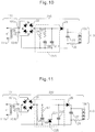
- Figure 9 is a detailed circuit diagram showing a circuit incorporating yet another alternative LED lighting circuit 200.
- the capacitor 68 when the capacitor 68 is formed from a tantalum capacitor, the effect of suppressing the noise can be further enhanced. However, since the rated voltage of a tantalum capacitor is low, there arises the possibility that the rated voltage may momentarily be exceeded. To address this, in the LED lighting circuit 200 shown in Figure 9 , the Zener diode 201 is inserted in parallel with the capacitor 68, a tantalum capacitor, to provide protection so that a voltage greater than the rated voltage will not be applied to the capacitor 68 momentarily.
- the Zener diode 201 may be inserted if it is required to reduce the overall circuit size, requiring the use of a capacitor with a low breakdown strength; in this case also, the provision of the Zener diode 201 offers the advantage of being able to achieve the effect of enhancing the breakdown strength and noise suppression.
- the circuit shown in Figure 9 can be incorporated in the LED illumination device shown in Figure 4 .
- the circuit shown in Figure 9 can also be incorporated in the illumination device/socket combination shown in Figure 5 .
- FIG. 10 is a detailed circuit diagram showing a circuit incorporating a further alternative LED lighting circuit 210.
- the ceramic capacitor 211 is inserted in parallel with the capacitor 68 so that the parallel circuit can operate stably as intended.
- the capacitance of the ceramic capacitor 211 is large, the ceramic capacitor 211 itself may cause noise. It is therefore preferable that the capacitance of the ceramic capacitor 211 is held to several tens of nanofarads.
- the circuit shown in Figure 10 can be incorporated in the LED illumination device shown in Figure 4 .
- the circuit shown in Figure 10 can also be incorporated in the illumination device/socket combination shown in Figure 5 .
- Figure 11 is a detailed circuit diagram showing a circuit incorporating a still further alternative LED lighting circuit 220.
- Zener diode 221 is inserted in parallel with the capacitor 68, a tantalum capacitor, is to provide protection so that a voltage greater than the rated voltage will not be applied to the capacitor 68 momentarily, as earlier described with reference to the circuit of Figure 9 .
- the reason that the ceramic capacitor 222 is inserted in parallel with the series connection of the resistor 67 and capacitor 68 is to ensure that the parallel circuit will operate stably as intended, as earlier described with reference to the circuit of Figure 10 . It is preferable that the capacitance of the ceramic capacitor 222 is held to several tens of nanofarads.
- the circuit shown in Figure 11 can be incorporated in the LED illumination device shown in Figure 4 .
- the circuit shown in Figure 11 can also be incorporated in the illumination device/socket combination shown in Figure 5 .
Landscapes
- Engineering & Computer Science (AREA)
- Power Engineering (AREA)
- Circuit Arrangement For Electric Light Sources In General (AREA)
Claims (10)
- Leuchtdioden(LED)-Beleuchtungsschaltung (100) zum Anschalten einer LED (105), umfassend:einen Gleichrichterschaltkreis (101) zum Gleichrichten einer Wechselstrom(AC)-Ausgabe von einer Wechselstromversorgung,eine LED-Treibereinheit (104), die als Eingabe eine gleichgerichtete Ausgabe von dem Gleichrichterschaltkreis aufnimmt und die LED treibt,eine Rückstromblockiereinheit (103), die zwischen dem Gleichrichterschaltkreis und der LED-Treibereinheit vorgesehen ist, undeine Anschlussspannung-Steuerungseinheit (102) mit einem Kondensator (25),dadurch gekennzeichnet, dassdie Wechselstromversorgung einen Wechselrichter aufweist,die Anschlussspannung-Steuerungseinheit dazu ausgebildet ist, eine Ausgangsanschlussspannung des Gleichrichterschaltkreises zu verringern, um eine Oszillation des Wechselrichters durch Freisetzen von Ladung, die im Kondensator gespeichert ist, wiederherzustellen, wenn eine Wechselstromausgabe von der Wechselstromversorgung instabil oder unterbrochen wird, undwobei die Rückstromblockiereinheit von der LED-Treibereinheit zum Gleichrichterschaltkreis fließenden Strom blockiert, wenn die Anschlussspannung-Steuerungseinheit zur Verringerung einer Ausgangsanschlussspannung des Gleichrichterschaltkreises wirksam ist.
- LED-Beleuchtungsschaltung nach Anspruch 1, wobei die Anschlussspannung-Steuerungseinheit als Parallelschaltung ausgebildet ist, die den Kondensator (25) und einen Widerstand (24) aufweist.
- LED-Beleuchtungsschaltung nach Anspruch 1 oder 2, wobei der Kondensator (25) in der Anschlussspannung-Steuerungseinheit als Tantal-Kondensator oder als Elektrolyt-Kondensator ausgebildet ist.
- LED-Beleuchtungsschaltung nach Anspruch 3, wobei die Anschlussspannung-Steuerungseinheit einen Widerstand (67, 72) aufweist, der mit dem Kondensator (68, 25) in Reihe geschaltet ist.
- LED-Beleuchtungsschaltung nach einem der Ansprüche 1 bis 4, wobei die Anschlussspannung-Steuerungseinheit eine Zener-Diode (201, 221) aufweist, die mit dem Kondensator (68) parallel geschaltet ist.
- LED-Beleuchtungsschaltung nach Anspruch 4, wobei die Anschlussspannung-Steuerungseinheit einen zweiten Kondensator (27) aufweist, der parallel geschaltet ist mit dem Kondensator und dem Widerstand, der mit dem Kondensator in Reihe geschaltet ist.
- LED-Beleuchtungsschaltung nach einem der Ansprüche 1 bis 6, wobei, wenn die Ausgabe des Gleichrichterschaltkreises unterbrochen wird, der Kondensator mit einer Zeitkonstante entladen wird, die länger als zwei Perioden der Wechselstromausgabe der Wechselstromversorgung eingestellt ist.
- LED-Beleuchtungsschaltung nach einem der Ansprüche 1 bis 7, wobei die Rückstromblockiereinheit eine Diode (26) aufweist.
- LED-Beleuchtungsvorrichtung versehen mit einer LED-Beleuchtungsschaltung nach einem der Ansprüche 1 bis 8.
- Buchse (160) für eine Leuchtdioden(LED)-Beleuchtungseinheit, wobei die Buchse mit einer LED-Beleuchtungseinheit (150) verbindbar ist und die LED-Beleuchtungseinheit eine LED-Treibereinheit (104) zum Treiben einer LED (105) aufweist, wobei die Buchse für eine LED-Beleuchtungseinheit umfasst:einen Gleichrichterschaltkreis (101) zum Gleichrichten einer Wechselstrom(AC)-Ausgabe von einer Wechselstromversorgung und Zuführen einer gleichgerichteten Ausgabe zu der LED-Treibereinheit,eine Rückstromblockiereinheit (103), die zwischen dem Gleichrichterschaltkreis und der LED-Treibereinheit vorgesehen ist, undeine Anschlussspannung-Steuerungseinheit (102) mit einem Kondensator (25),dadurch gekennzeichnet, dassdie Wechselstromversorgung einen Wechselrichter aufweist,die Anschlussspannung-Steuerungseinheit dazu ausgebildet ist, eine Ausgangsanschlussspannung des Gleichrichterschaltkreises zu verringern, um eine Oszillation des Wechselrichters durch Freisetzen von Ladung, die im Kondensator gespeichert ist, wiederherzustellen, wenn eine Wechselstromausgabe von der Wechselstromversorgung instabil oder unterbrochen wird, undwobei die Rückstromblockiereinheit von der LED-Treibereinheit zum Gleichrichterschaltkreis fließenden Strom blockiert, wenn die Anschlussspannung-Steuerungseinheit zur Verringerung einer Ausgangsanschlussspannung des Gleichrichterschaltkreises wirksam ist.
Applications Claiming Priority (4)
| Application Number | Priority Date | Filing Date | Title |
|---|---|---|---|
| JP2010241943 | 2010-10-28 | ||
| JP2010263492 | 2010-11-26 | ||
| JP2010269223 | 2010-12-02 | ||
| PCT/JP2011/075368 WO2012057369A1 (ja) | 2010-10-28 | 2011-10-27 | Led点灯回路、led照明装置、及びled照明部用ソケット |
Publications (3)
| Publication Number | Publication Date |
|---|---|
| EP2634823A1 EP2634823A1 (de) | 2013-09-04 |
| EP2634823A4 EP2634823A4 (de) | 2017-06-21 |
| EP2634823B1 true EP2634823B1 (de) | 2019-05-08 |
Family
ID=45994066
Family Applications (1)
| Application Number | Title | Priority Date | Filing Date |
|---|---|---|---|
| EP11836498.3A Not-in-force EP2634823B1 (de) | 2010-10-28 | 2011-10-27 | Led-beleuchtungsschaltung, led-beleuchtungsvorrichtung und buchse für eine led-beleuchtungseinheit |
Country Status (5)
| Country | Link |
|---|---|
| US (1) | US9226364B2 (de) |
| EP (1) | EP2634823B1 (de) |
| JP (1) | JP5921438B2 (de) |
| CN (1) | CN103190002B (de) |
| WO (1) | WO2012057369A1 (de) |
Families Citing this family (15)
| Publication number | Priority date | Publication date | Assignee | Title |
|---|---|---|---|---|
| CN102858076B (zh) * | 2012-10-24 | 2014-09-10 | 东莞健达照明有限公司 | 一种可兼容电子变压器的led射灯电路 |
| KR101559986B1 (ko) * | 2013-08-01 | 2015-10-14 | 주식회사 파워넷 | 조명장치를 구동하는 장치 |
| JP6164413B2 (ja) * | 2013-08-12 | 2017-07-19 | ウシオ電機株式会社 | 電源装置及び電源装置の改良方法 |
| US20150173150A1 (en) * | 2013-12-17 | 2015-06-18 | Altoran Chips & Systems | Balanced AC Direct Driver Lighting System with a Valley Fill Circuit and a Light Balancer |
| CN104093255B (zh) * | 2014-07-23 | 2016-03-09 | 深圳市凯信光电有限公司 | Led智能照明系统的控制方法 |
| ES2644863T3 (es) * | 2015-06-04 | 2017-11-30 | Philips Lighting Holding B.V. | Fuente de luz LED con reducción de luminiscencia mejorada |
| JP6823917B2 (ja) * | 2015-07-31 | 2021-02-03 | アール・ビー・コントロールズ株式会社 | Led照明装置 |
| JP6542604B2 (ja) * | 2015-08-07 | 2019-07-10 | ウシオ電機株式会社 | Ledランプ |
| CN105430810A (zh) * | 2015-12-25 | 2016-03-23 | 电子科技大学 | 一种led照明驱动系统 |
| CN105392240A (zh) * | 2015-12-25 | 2016-03-09 | 电子科技大学 | 一种led照明驱动系统 |
| CN105592598B (zh) * | 2016-03-21 | 2018-02-13 | 上海路傲电子科技有限公司 | 高功率因数、无频闪的led驱动电路 |
| JP6786060B2 (ja) * | 2016-06-20 | 2020-11-18 | 株式会社キルトプランニングオフィス | 有機el発光システム |
| US10674585B1 (en) * | 2019-04-30 | 2020-06-02 | Ledvance Llc | Reliability of hardware reset process for smart light emitting diode (LED) bulbs |
| CN114189958B (zh) * | 2021-11-01 | 2024-10-29 | 广州市浩洋电子股份有限公司 | 一种利用抑振模块减少光源低亮抖动的装置和灯具 |
| KR102382016B1 (ko) | 2021-11-02 | 2022-04-04 | 주식회사 웰랑 | 높은 led 활용도를 제공하는 장치 및 이를 포함하는 조명 기기 |
Family Cites Families (20)
| Publication number | Priority date | Publication date | Assignee | Title |
|---|---|---|---|---|
| JP2770337B2 (ja) | 1988-08-31 | 1998-07-02 | 岩崎電気株式会社 | 点灯装置 |
| US5373215A (en) * | 1993-07-07 | 1994-12-13 | The United States Of America As Represented By The United States Department Of Energy | Ionization tube simmer current circuit |
| JP4353667B2 (ja) * | 1999-12-14 | 2009-10-28 | 株式会社タキオン | Ledランプ装置 |
| JP4449333B2 (ja) * | 2003-04-30 | 2010-04-14 | 東芝ライテック株式会社 | Led点灯装置およびled標識灯 |
| US7978485B2 (en) * | 2007-05-04 | 2011-07-12 | Stmicroelectronics, Inc. | Thyristor power control circuit with damping circuit maintaining thyristor holding current |
| US20100207536A1 (en) * | 2007-10-26 | 2010-08-19 | Lighting Science Group Corporation | High efficiency light source with integrated ballast |
| JP2009302017A (ja) | 2008-06-17 | 2009-12-24 | Toshiba Lighting & Technology Corp | 発光ダイオード点灯装置および照明装置 |
| JP5345810B2 (ja) * | 2008-08-12 | 2013-11-20 | ローム株式会社 | 駆動装置 |
| JP5401937B2 (ja) * | 2008-11-12 | 2014-01-29 | 東芝ライテック株式会社 | 点灯装置および照明器具 |
| JP2010135139A (ja) | 2008-12-03 | 2010-06-17 | Ushio Inc | Led点灯回路及びledランプ並びにledランプ点灯用変換ソケット |
| KR101018114B1 (ko) * | 2008-12-22 | 2011-02-25 | 삼성전기주식회사 | 액정 표시 장치의 전원 공급 장치 |
| JP4630930B2 (ja) * | 2009-01-29 | 2011-02-09 | 極光電気株式会社 | Led駆動回路及びそれを用いたled照明装置 |
| KR101659715B1 (ko) * | 2009-06-18 | 2016-09-26 | 코닌클리케 필립스 엔.브이. | Triac 디머를 위한 led들을 갖는 파워 인터페이스 |
| CN101640966B (zh) * | 2009-09-07 | 2012-11-21 | 江阴瑞福得电器有限公司 | 一种荧光灯的供电电路 |
| JP5198405B2 (ja) * | 2009-10-22 | 2013-05-15 | フェニックス電機株式会社 | 電源回路 |
| JP5564239B2 (ja) * | 2009-12-14 | 2014-07-30 | ミネベア株式会社 | Led駆動回路 |
| JP2011233450A (ja) * | 2010-04-30 | 2011-11-17 | On Semiconductor Trading Ltd | 発光素子の制御回路 |
| CN103313472B (zh) * | 2010-05-19 | 2016-02-03 | 成都芯源系统有限公司 | 一种具有调光功能的led驱动电路及灯具 |
| KR20120056162A (ko) * | 2010-11-24 | 2012-06-01 | 삼성엘이디 주식회사 | Led 구동장치 |
| KR101065709B1 (ko) * | 2011-06-15 | 2011-09-19 | 엘지전자 주식회사 | 조명 제어 방법, 조명 장치 및 조명 시스템 |
-
2011
- 2011-10-27 US US13/881,724 patent/US9226364B2/en not_active Expired - Fee Related
- 2011-10-27 EP EP11836498.3A patent/EP2634823B1/de not_active Not-in-force
- 2011-10-27 WO PCT/JP2011/075368 patent/WO2012057369A1/ja not_active Ceased
- 2011-10-27 CN CN201180052559.3A patent/CN103190002B/zh not_active Expired - Fee Related
- 2011-10-27 JP JP2012540997A patent/JP5921438B2/ja not_active Expired - Fee Related
Non-Patent Citations (1)
| Title |
|---|
| None * |
Also Published As
| Publication number | Publication date |
|---|---|
| CN103190002A (zh) | 2013-07-03 |
| EP2634823A4 (de) | 2017-06-21 |
| JPWO2012057369A1 (ja) | 2014-05-12 |
| US20130221864A1 (en) | 2013-08-29 |
| EP2634823A1 (de) | 2013-09-04 |
| CN103190002B (zh) | 2016-02-17 |
| JP5921438B2 (ja) | 2016-05-24 |
| WO2012057369A1 (ja) | 2012-05-03 |
| US9226364B2 (en) | 2015-12-29 |
Similar Documents
| Publication | Publication Date | Title |
|---|---|---|
| EP2634823B1 (de) | Led-beleuchtungsschaltung, led-beleuchtungsvorrichtung und buchse für eine led-beleuchtungseinheit | |
| JP5632664B2 (ja) | 半導体発光素子の点灯装置およびそれを用いた照明器具 | |
| CN207124784U (zh) | 一种安装侦测模块的电路以及led直管灯 | |
| US8482214B2 (en) | Apparatus and methods of operation of passive LED lighting equipment | |
| JP5364897B2 (ja) | 電源装置及び照明器具 | |
| JP2008235530A (ja) | 発光ダイオード駆動装置、及びそれを用いた照明装置 | |
| CN211297077U (zh) | 一种安装状态的检测电路 | |
| CN102740555A (zh) | 用于固态光源的点亮装置和包括该点亮装置的照明设备 | |
| JP2011049527A (ja) | Led照明装置 | |
| JP5980107B2 (ja) | 電源装置及び照明装置 | |
| WO2011148590A1 (ja) | Ledの点灯回路、ランプおよび照明装置 | |
| JP2009302017A (ja) | 発光ダイオード点灯装置および照明装置 | |
| CN103546027A (zh) | 电源装置、固体发光元件点灯装置及照明装置 | |
| EP2710860A2 (de) | Nachrüstbare led-treiberschaltung und betriebsverfahren dafür | |
| US20100270930A1 (en) | Apparatus and methods of operation of passive led lighting equipment | |
| US9544959B2 (en) | Solid-state lighting compatible with ballasts and operable with AC mains | |
| CN103959915A (zh) | 用于降压转换器的起动电路 | |
| US20100270931A1 (en) | Apparatus and methods of operation of passive led lighting equipment | |
| CN1615066B (zh) | 具有灯故障时继续工作的转换器的电子镇流器及工作方法 | |
| CN211959612U (zh) | 一种led直管灯及其电源模块和一种led照明系统 | |
| KR20140049841A (ko) | Led 조명등용 전원 공급 장치 및 그 방법과 그를 이용한 led 조명 장치 | |
| JP2013229975A (ja) | スイッチング電源装置および発光装置 | |
| JP5857252B2 (ja) | 点灯回路およびこれを備えたランプ | |
| CN211481558U (zh) | 一种led直管灯、电源模块及其滤波电路与安装侦测模块 | |
| JP2012169183A (ja) | 調光型点灯回路 |
Legal Events
| Date | Code | Title | Description |
|---|---|---|---|
| PUAI | Public reference made under article 153(3) epc to a published international application that has entered the european phase |
Free format text: ORIGINAL CODE: 0009012 |
|
| 17P | Request for examination filed |
Effective date: 20130416 |
|
| AK | Designated contracting states |
Kind code of ref document: A1 Designated state(s): AL AT BE BG CH CY CZ DE DK EE ES FI FR GB GR HR HU IE IS IT LI LT LU LV MC MK MT NL NO PL PT RO RS SE SI SK SM TR |
|
| DAX | Request for extension of the european patent (deleted) | ||
| RAP1 | Party data changed (applicant data changed or rights of an application transferred) |
Owner name: CITIZEN WATCH CO., LTD. Owner name: CITIZEN ELECTRONICS CO., LTD. |
|
| RA4 | Supplementary search report drawn up and despatched (corrected) |
Effective date: 20170523 |
|
| RIC1 | Information provided on ipc code assigned before grant |
Ipc: H02M 7/06 20060101ALI20170517BHEP Ipc: H05B 33/08 20060101AFI20170517BHEP |
|
| REG | Reference to a national code |
Ref country code: DE Ref legal event code: R079 Ref document number: 602011058862 Country of ref document: DE Free format text: PREVIOUS MAIN CLASS: H01L0033000000 Ipc: H05B0033080000 |
|
| GRAP | Despatch of communication of intention to grant a patent |
Free format text: ORIGINAL CODE: EPIDOSNIGR1 |
|
| STAA | Information on the status of an ep patent application or granted ep patent |
Free format text: STATUS: GRANT OF PATENT IS INTENDED |
|
| RIC1 | Information provided on ipc code assigned before grant |
Ipc: H02M 7/5383 20070101ALI20181102BHEP Ipc: H05B 33/08 20060101AFI20181102BHEP Ipc: H02M 7/06 20060101ALI20181102BHEP |
|
| INTG | Intention to grant announced |
Effective date: 20181203 |
|
| RIN1 | Information on inventor provided before grant (corrected) |
Inventor name: AKIYAMA, TAKASHI Inventor name: FUKASAWA, HISASHI |
|
| GRAS | Grant fee paid |
Free format text: ORIGINAL CODE: EPIDOSNIGR3 |
|
| GRAA | (expected) grant |
Free format text: ORIGINAL CODE: 0009210 |
|
| STAA | Information on the status of an ep patent application or granted ep patent |
Free format text: STATUS: THE PATENT HAS BEEN GRANTED |
|
| AK | Designated contracting states |
Kind code of ref document: B1 Designated state(s): AL AT BE BG CH CY CZ DE DK EE ES FI FR GB GR HR HU IE IS IT LI LT LU LV MC MK MT NL NO PL PT RO RS SE SI SK SM TR |
|
| REG | Reference to a national code |
Ref country code: GB Ref legal event code: FG4D |
|
| REG | Reference to a national code |
Ref country code: CH Ref legal event code: EP Ref country code: AT Ref legal event code: REF Ref document number: 1132260 Country of ref document: AT Kind code of ref document: T Effective date: 20190515 |
|
| REG | Reference to a national code |
Ref country code: DE Ref legal event code: R096 Ref document number: 602011058862 Country of ref document: DE Ref country code: IE Ref legal event code: FG4D |
|
| REG | Reference to a national code |
Ref country code: NL Ref legal event code: MP Effective date: 20190508 |
|
| REG | Reference to a national code |
Ref country code: LT Ref legal event code: MG4D |
|
| PG25 | Lapsed in a contracting state [announced via postgrant information from national office to epo] |
Ref country code: NO Free format text: LAPSE BECAUSE OF FAILURE TO SUBMIT A TRANSLATION OF THE DESCRIPTION OR TO PAY THE FEE WITHIN THE PRESCRIBED TIME-LIMIT Effective date: 20190808 Ref country code: FI Free format text: LAPSE BECAUSE OF FAILURE TO SUBMIT A TRANSLATION OF THE DESCRIPTION OR TO PAY THE FEE WITHIN THE PRESCRIBED TIME-LIMIT Effective date: 20190508 Ref country code: LT Free format text: LAPSE BECAUSE OF FAILURE TO SUBMIT A TRANSLATION OF THE DESCRIPTION OR TO PAY THE FEE WITHIN THE PRESCRIBED TIME-LIMIT Effective date: 20190508 Ref country code: HR Free format text: LAPSE BECAUSE OF FAILURE TO SUBMIT A TRANSLATION OF THE DESCRIPTION OR TO PAY THE FEE WITHIN THE PRESCRIBED TIME-LIMIT Effective date: 20190508 Ref country code: PT Free format text: LAPSE BECAUSE OF FAILURE TO SUBMIT A TRANSLATION OF THE DESCRIPTION OR TO PAY THE FEE WITHIN THE PRESCRIBED TIME-LIMIT Effective date: 20190908 Ref country code: SE Free format text: LAPSE BECAUSE OF FAILURE TO SUBMIT A TRANSLATION OF THE DESCRIPTION OR TO PAY THE FEE WITHIN THE PRESCRIBED TIME-LIMIT Effective date: 20190508 Ref country code: AL Free format text: LAPSE BECAUSE OF FAILURE TO SUBMIT A TRANSLATION OF THE DESCRIPTION OR TO PAY THE FEE WITHIN THE PRESCRIBED TIME-LIMIT Effective date: 20190508 Ref country code: NL Free format text: LAPSE BECAUSE OF FAILURE TO SUBMIT A TRANSLATION OF THE DESCRIPTION OR TO PAY THE FEE WITHIN THE PRESCRIBED TIME-LIMIT Effective date: 20190508 Ref country code: ES Free format text: LAPSE BECAUSE OF FAILURE TO SUBMIT A TRANSLATION OF THE DESCRIPTION OR TO PAY THE FEE WITHIN THE PRESCRIBED TIME-LIMIT Effective date: 20190508 |
|
| REG | Reference to a national code |
Ref country code: DE Ref legal event code: R079 Ref document number: 602011058862 Country of ref document: DE Free format text: PREVIOUS MAIN CLASS: H05B0033080000 Ipc: H05B0045000000 |
|
| PG25 | Lapsed in a contracting state [announced via postgrant information from national office to epo] |
Ref country code: LV Free format text: LAPSE BECAUSE OF FAILURE TO SUBMIT A TRANSLATION OF THE DESCRIPTION OR TO PAY THE FEE WITHIN THE PRESCRIBED TIME-LIMIT Effective date: 20190508 Ref country code: BG Free format text: LAPSE BECAUSE OF FAILURE TO SUBMIT A TRANSLATION OF THE DESCRIPTION OR TO PAY THE FEE WITHIN THE PRESCRIBED TIME-LIMIT Effective date: 20190808 Ref country code: RS Free format text: LAPSE BECAUSE OF FAILURE TO SUBMIT A TRANSLATION OF THE DESCRIPTION OR TO PAY THE FEE WITHIN THE PRESCRIBED TIME-LIMIT Effective date: 20190508 Ref country code: GR Free format text: LAPSE BECAUSE OF FAILURE TO SUBMIT A TRANSLATION OF THE DESCRIPTION OR TO PAY THE FEE WITHIN THE PRESCRIBED TIME-LIMIT Effective date: 20190809 |
|
| REG | Reference to a national code |
Ref country code: AT Ref legal event code: MK05 Ref document number: 1132260 Country of ref document: AT Kind code of ref document: T Effective date: 20190508 |
|
| PG25 | Lapsed in a contracting state [announced via postgrant information from national office to epo] |
Ref country code: RO Free format text: LAPSE BECAUSE OF FAILURE TO SUBMIT A TRANSLATION OF THE DESCRIPTION OR TO PAY THE FEE WITHIN THE PRESCRIBED TIME-LIMIT Effective date: 20190508 Ref country code: SK Free format text: LAPSE BECAUSE OF FAILURE TO SUBMIT A TRANSLATION OF THE DESCRIPTION OR TO PAY THE FEE WITHIN THE PRESCRIBED TIME-LIMIT Effective date: 20190508 Ref country code: DK Free format text: LAPSE BECAUSE OF FAILURE TO SUBMIT A TRANSLATION OF THE DESCRIPTION OR TO PAY THE FEE WITHIN THE PRESCRIBED TIME-LIMIT Effective date: 20190508 Ref country code: AT Free format text: LAPSE BECAUSE OF FAILURE TO SUBMIT A TRANSLATION OF THE DESCRIPTION OR TO PAY THE FEE WITHIN THE PRESCRIBED TIME-LIMIT Effective date: 20190508 Ref country code: EE Free format text: LAPSE BECAUSE OF FAILURE TO SUBMIT A TRANSLATION OF THE DESCRIPTION OR TO PAY THE FEE WITHIN THE PRESCRIBED TIME-LIMIT Effective date: 20190508 Ref country code: CZ Free format text: LAPSE BECAUSE OF FAILURE TO SUBMIT A TRANSLATION OF THE DESCRIPTION OR TO PAY THE FEE WITHIN THE PRESCRIBED TIME-LIMIT Effective date: 20190508 |
|
| PGFP | Annual fee paid to national office [announced via postgrant information from national office to epo] |
Ref country code: DE Payment date: 20191023 Year of fee payment: 9 |
|
| REG | Reference to a national code |
Ref country code: DE Ref legal event code: R097 Ref document number: 602011058862 Country of ref document: DE |
|
| PG25 | Lapsed in a contracting state [announced via postgrant information from national office to epo] |
Ref country code: IT Free format text: LAPSE BECAUSE OF FAILURE TO SUBMIT A TRANSLATION OF THE DESCRIPTION OR TO PAY THE FEE WITHIN THE PRESCRIBED TIME-LIMIT Effective date: 20190508 Ref country code: SM Free format text: LAPSE BECAUSE OF FAILURE TO SUBMIT A TRANSLATION OF THE DESCRIPTION OR TO PAY THE FEE WITHIN THE PRESCRIBED TIME-LIMIT Effective date: 20190508 |
|
| PLBE | No opposition filed within time limit |
Free format text: ORIGINAL CODE: 0009261 |
|
| STAA | Information on the status of an ep patent application or granted ep patent |
Free format text: STATUS: NO OPPOSITION FILED WITHIN TIME LIMIT |
|
| PG25 | Lapsed in a contracting state [announced via postgrant information from national office to epo] |
Ref country code: TR Free format text: LAPSE BECAUSE OF FAILURE TO SUBMIT A TRANSLATION OF THE DESCRIPTION OR TO PAY THE FEE WITHIN THE PRESCRIBED TIME-LIMIT Effective date: 20190508 |
|
| 26N | No opposition filed |
Effective date: 20200211 |
|
| PG25 | Lapsed in a contracting state [announced via postgrant information from national office to epo] |
Ref country code: PL Free format text: LAPSE BECAUSE OF FAILURE TO SUBMIT A TRANSLATION OF THE DESCRIPTION OR TO PAY THE FEE WITHIN THE PRESCRIBED TIME-LIMIT Effective date: 20190508 |
|
| PG25 | Lapsed in a contracting state [announced via postgrant information from national office to epo] |
Ref country code: SI Free format text: LAPSE BECAUSE OF FAILURE TO SUBMIT A TRANSLATION OF THE DESCRIPTION OR TO PAY THE FEE WITHIN THE PRESCRIBED TIME-LIMIT Effective date: 20190508 Ref country code: MC Free format text: LAPSE BECAUSE OF FAILURE TO SUBMIT A TRANSLATION OF THE DESCRIPTION OR TO PAY THE FEE WITHIN THE PRESCRIBED TIME-LIMIT Effective date: 20190508 |
|
| REG | Reference to a national code |
Ref country code: CH Ref legal event code: PL |
|
| PG25 | Lapsed in a contracting state [announced via postgrant information from national office to epo] |
Ref country code: LI Free format text: LAPSE BECAUSE OF NON-PAYMENT OF DUE FEES Effective date: 20191031 Ref country code: CH Free format text: LAPSE BECAUSE OF NON-PAYMENT OF DUE FEES Effective date: 20191031 Ref country code: LU Free format text: LAPSE BECAUSE OF NON-PAYMENT OF DUE FEES Effective date: 20191027 |
|
| REG | Reference to a national code |
Ref country code: BE Ref legal event code: MM Effective date: 20191031 |
|
| PG25 | Lapsed in a contracting state [announced via postgrant information from national office to epo] |
Ref country code: BE Free format text: LAPSE BECAUSE OF NON-PAYMENT OF DUE FEES Effective date: 20191031 |
|
| GBPC | Gb: european patent ceased through non-payment of renewal fee |
Effective date: 20191027 |
|
| PG25 | Lapsed in a contracting state [announced via postgrant information from national office to epo] |
Ref country code: FR Free format text: LAPSE BECAUSE OF NON-PAYMENT OF DUE FEES Effective date: 20191031 Ref country code: GB Free format text: LAPSE BECAUSE OF NON-PAYMENT OF DUE FEES Effective date: 20191027 Ref country code: IE Free format text: LAPSE BECAUSE OF NON-PAYMENT OF DUE FEES Effective date: 20191027 |
|
| REG | Reference to a national code |
Ref country code: DE Ref legal event code: R119 Ref document number: 602011058862 Country of ref document: DE |
|
| PG25 | Lapsed in a contracting state [announced via postgrant information from national office to epo] |
Ref country code: CY Free format text: LAPSE BECAUSE OF FAILURE TO SUBMIT A TRANSLATION OF THE DESCRIPTION OR TO PAY THE FEE WITHIN THE PRESCRIBED TIME-LIMIT Effective date: 20190508 |
|
| PG25 | Lapsed in a contracting state [announced via postgrant information from national office to epo] |
Ref country code: IS Free format text: LAPSE BECAUSE OF FAILURE TO SUBMIT A TRANSLATION OF THE DESCRIPTION OR TO PAY THE FEE WITHIN THE PRESCRIBED TIME-LIMIT Effective date: 20190908 |
|
| PG25 | Lapsed in a contracting state [announced via postgrant information from national office to epo] |
Ref country code: HU Free format text: LAPSE BECAUSE OF FAILURE TO SUBMIT A TRANSLATION OF THE DESCRIPTION OR TO PAY THE FEE WITHIN THE PRESCRIBED TIME-LIMIT; INVALID AB INITIO Effective date: 20111027 Ref country code: MT Free format text: LAPSE BECAUSE OF FAILURE TO SUBMIT A TRANSLATION OF THE DESCRIPTION OR TO PAY THE FEE WITHIN THE PRESCRIBED TIME-LIMIT Effective date: 20190508 Ref country code: DE Free format text: LAPSE BECAUSE OF NON-PAYMENT OF DUE FEES Effective date: 20210501 |
|
| PG25 | Lapsed in a contracting state [announced via postgrant information from national office to epo] |
Ref country code: MK Free format text: LAPSE BECAUSE OF FAILURE TO SUBMIT A TRANSLATION OF THE DESCRIPTION OR TO PAY THE FEE WITHIN THE PRESCRIBED TIME-LIMIT Effective date: 20190508 |