EP2634864A2 - Dispositif à plaquettes et agencement électrique correspondant - Google Patents
Dispositif à plaquettes et agencement électrique correspondant Download PDFInfo
- Publication number
- EP2634864A2 EP2634864A2 EP13153090.9A EP13153090A EP2634864A2 EP 2634864 A2 EP2634864 A2 EP 2634864A2 EP 13153090 A EP13153090 A EP 13153090A EP 2634864 A2 EP2634864 A2 EP 2634864A2
- Authority
- EP
- European Patent Office
- Prior art keywords
- circuit board
- spring element
- printed circuit
- plug
- force
- Prior art date
- Legal status (The legal status is an assumption and is not a legal conclusion. Google has not performed a legal analysis and makes no representation as to the accuracy of the status listed.)
- Granted
Links
- 239000004020 conductor Substances 0.000 claims abstract description 30
- 239000000758 substrate Substances 0.000 claims abstract description 15
- 229910052751 metal Inorganic materials 0.000 claims abstract description 6
- 239000002184 metal Substances 0.000 claims abstract description 6
- 229910001092 metal group alloy Inorganic materials 0.000 claims abstract description 4
- 210000002105 tongue Anatomy 0.000 claims 1
- 239000004033 plastic Substances 0.000 description 4
- 229920003023 plastic Polymers 0.000 description 4
- 238000004519 manufacturing process Methods 0.000 description 3
- 230000007423 decrease Effects 0.000 description 2
- 238000009826 distribution Methods 0.000 description 2
- 239000000463 material Substances 0.000 description 2
- 239000010935 stainless steel Substances 0.000 description 2
- 229910001220 stainless steel Inorganic materials 0.000 description 2
- 230000007704 transition Effects 0.000 description 2
- 229910045601 alloy Inorganic materials 0.000 description 1
- 239000000956 alloy Substances 0.000 description 1
- 239000000919 ceramic Substances 0.000 description 1
- 230000003247 decreasing effect Effects 0.000 description 1
- 230000001419 dependent effect Effects 0.000 description 1
- 239000004744 fabric Substances 0.000 description 1
- 239000003365 glass fiber Substances 0.000 description 1
- 238000003780 insertion Methods 0.000 description 1
- 230000037431 insertion Effects 0.000 description 1
- 239000011810 insulating material Substances 0.000 description 1
- 238000005304 joining Methods 0.000 description 1
- 150000002739 metals Chemical class 0.000 description 1
- 238000002360 preparation method Methods 0.000 description 1
- 238000005476 soldering Methods 0.000 description 1
- 239000003053 toxin Substances 0.000 description 1
- 231100000765 toxin Toxicity 0.000 description 1
- 108700012359 toxins Proteins 0.000 description 1
- 238000003466 welding Methods 0.000 description 1
Images


Classifications
-
- H—ELECTRICITY
- H01—ELECTRIC ELEMENTS
- H01R—ELECTRICALLY-CONDUCTIVE CONNECTIONS; STRUCTURAL ASSOCIATIONS OF A PLURALITY OF MUTUALLY-INSULATED ELECTRICAL CONNECTING ELEMENTS; COUPLING DEVICES; CURRENT COLLECTORS
- H01R12/00—Structural associations of a plurality of mutually-insulated electrical connecting elements, specially adapted for printed circuits, e.g. printed circuit boards [PCB], flat or ribbon cables, or like generally planar structures, e.g. terminal strips, terminal blocks; Coupling devices specially adapted for printed circuits, flat or ribbon cables, or like generally planar structures; Terminals specially adapted for contact with, or insertion into, printed circuits, flat or ribbon cables, or like generally planar structures
- H01R12/70—Coupling devices
- H01R12/71—Coupling devices for rigid printing circuits or like structures
- H01R12/72—Coupling devices for rigid printing circuits or like structures coupling with the edge of the rigid printed circuits or like structures
- H01R12/721—Coupling devices for rigid printing circuits or like structures coupling with the edge of the rigid printed circuits or like structures cooperating directly with the edge of the rigid printed circuits
-
- H—ELECTRICITY
- H01—ELECTRIC ELEMENTS
- H01R—ELECTRICALLY-CONDUCTIVE CONNECTIONS; STRUCTURAL ASSOCIATIONS OF A PLURALITY OF MUTUALLY-INSULATED ELECTRICAL CONNECTING ELEMENTS; COUPLING DEVICES; CURRENT COLLECTORS
- H01R12/00—Structural associations of a plurality of mutually-insulated electrical connecting elements, specially adapted for printed circuits, e.g. printed circuit boards [PCB], flat or ribbon cables, or like generally planar structures, e.g. terminal strips, terminal blocks; Coupling devices specially adapted for printed circuits, flat or ribbon cables, or like generally planar structures; Terminals specially adapted for contact with, or insertion into, printed circuits, flat or ribbon cables, or like generally planar structures
- H01R12/70—Coupling devices
- H01R12/82—Coupling devices connected with low or zero insertion force
- H01R12/85—Coupling devices connected with low or zero insertion force contact pressure producing means, contacts activated after insertion of printed circuits or like structures
Definitions
- direct plug-in connectors or connectors are contacted directly on the printed circuit board without additional pin headers.
- the plugs are usually attached to the edge-mounted contact pads on the circuit boards.
- the contact pads can be integrated on the PCB top side as well as on the underside of the PCB in the PCB layout.
- the contact pads are usually formed from the mechanically firmly connected to an electrically insulating substrate of the circuit board interconnects.
- the plug consist essentially of a plug housing and a contact element, wherein in the attached state, the contact element is pressed by a spring force against the contact pad.
- the contact element is in this case usually resilient, so that the contact element for applying the spring force to the conductor track, respectively on the contact pad on which made of an insulating material, usually made of plastic, plug housing of the plug is supported.
- a printed circuit board device comprising a printed circuit board with an electrically insulating substrate and at least one electrically conductive conductor track.
- the conductor track is firmly connected to the substrate.
- the conductor extends along a longitudinal direction of the substrate.
- a plug having a plug housing and an electrical contact element arranged in the plug housing can be electrically conductively connected to the printed circuit board.
- a spring element is firmly connected. When the plug is connected to the printed circuit board, the spring element exerts a force on the plug housing substantially perpendicular to the printed circuit board in order to press the electrical contact element onto the printed conductor.
- the contact element may be resilient or designed only as a rigid plate.
- the contact element when the contact element is resilient, the relaxation of the plug housing and thus decreasing the conductor track pressure force is compensated for by the fact that the spring element presses the plug housing and thus the contact element to the circuit board.
- the spring element is thus ensured that the contact element is secured to the conductor over the calculated lifetime of the PCB-connector connection.
- the printed circuit board can be made of resin-impregnated glass fiber fabric in a quality of FR4 or higher.
- the electrically non-conductive substrate may be made of ceramic.
- the conductor can also be formed as a stamped grid. The force acting perpendicular to the circuit board of the spring element does not necessarily have to be introduced into the circuit board.
- the force introduced into the spring element can be supported on a carrier element, wherein the circuit board may be connected to the carrier element without supporting the carrier element.
- the spring element can also be connected to the printed circuit board in such a way that the force acting on the spring element is conducted into the printed circuit board.
- the connector housing has a groove.
- the plug When the plug is connected to the circuit board, a portion of the circuit board is covered by the groove.
- the electrical contact element can be supported on the connector housing to be resiliently pressed against the conductor track.
- the spring element can be arranged with respect to the circuit board such that the contact elements are already connected to the conductor track before the spring element is in engagement with the connector housing. This can be avoided in an advantageous manner, damage to the surface of the contact elements and / or the conductor, which is often due to the high pressure force of the contact elements of the known direct connector, which already acts upon pushing of these contact elements on the conductor track. It may therefore, for example, the contact element be designed to be slightly resilient so as to perform a pre-positioning of the plug housing when pushed onto the conductor track, while the contact pressure for reliable electrical contacting of the contact elements is effected by the spring element.
- the spring element has at least in a partial area substantially a Z-shape with a first leg member, a second leg member and a first leg member and the second leg member with each other inseparably connecting first web element.
- the first leg member is connected to the circuit board.
- the second leg member exerts the force on the plug.
- the circuit board may be designed such that the forces acting on the circuit board in the longitudinal direction of the circuit board or perpendicular to the Printed circuit board, are absorbed by the circuit board.
- the circuit board may also be designed such that only a force in the longitudinal direction of the circuit board is received.
- the spring element can in this case be arranged on a first side of the printed circuit board, whereas the force acting through the plug on the spring element perpendicular to the longitudinal direction of the circuit board force can be introduced into a receiving element, wherein the receiving element on one of the first side of the circuit board opposite second side of Printed circuit board can be arranged.
- the circuit board may be fixed to the receiving element such that no forces must be absorbed by the spring element through the circuit board.
- the circuit board can be free from the forces generated by the spring element.
- the second leg member is formed substantially S-shaped with a first bay and a second bay.
- the first bay is firmly connected to the web element.
- the second bay exerts the force on the plug.
- the force is applied linearly to the connector housing.
- the second leg member is connected by means of a first bay to the web element, the force is entered by the second leg member in the web element arcuate.
- the second leg element has at least one cut, so that the second leg element has at least two independent resilient spring lamellae.
- the circuit board device further comprises a second spring element.
- the first spring element and the second spring element are firmly connected to one another such that when the plug is connected to the printed circuit board, the second spring element exerts a second force on the plug substantially perpendicular to the printed circuit board.
- the second spring element is configured such that the first force and the second force are substantially equal.
- the plug housing is encompassed and pressed the contact elements to the respective conductor tracks.
- the connector housing can be configured reversibly elastically deformable, so that the connector housing is deformed by the two counteracting forces such that the electrical contact element are pressed by the two spring elements to the conductor track.
- the conductor tracks are arranged both on a first side of the electrically insulating substrate and a second side of the substrate opposite the first side, it is achieved by such an arrangement that both the first side facing contact elements and those facing the second side Contact elements of the connector are pressed against the conductor tracks.
- the first spring element and the second spring element may be connected to one another by soldering, screwing, riveting, welding or clinching.
- the first spring element and the second spring element are substantially equal to each other when the plug housing is configured with respect to a mirror formed in the plug housing mirror image.
- the first spring element and the second spring element are rigidly connected to one another with respect to the printed circuit board.
- the first spring element and the second spring element can be manufactured in a tool.
- the groove when the plug is connected to the circuit board is connected, comprising a portion of the circuit board. Due to the rigid connection, both spring elements can exert a force on the plug housing.
- the second spring element is formed substantially L-shaped with a third leg member and a non-detachably connected to the third leg member second web member.
- the second web element and the first web element are non-releasably rigidly connected to each other.
- the first force is introduced via the second leg element into the first web element and the second force via the third leg element into the second web element.
- the two web elements are rigidly connected to each other in such a way that the forces introduced into the web elements over the entire service life of the printed circuit board / plug combination can not damage this connection.
- the first spring element and the second spring element made of metal or a metal alloy.
- metals or metal alloys which have resilient properties such as, for example, cold-rolled, as a rule, stainless steel sheets, are suitable for this purpose.
- metal or its alloys has no relaxation behavior, as is known from plastics.
- the spring made of metal spring elements can ensure over the entire life of the PCB-plug combination that the contact elements are pressed electrically conductive to the tracks.
- the first spring element or the second spring element or a combination of the first spring element and the second spring element is in one piece.
- the one-piece design eliminates further steps for the preparation of the individual spring elements. Thus, it is possible that only with the use of a tool first spring elements or second Spring elements or a combination of the first spring element and the second spring element can be manufactured.
- an electrical arrangement is provided with a printed circuit board device and a plug as described above.
- the plug is electrically conductively connected to the circuit board.
- At least one component of the group of first spring element and second spring element exerts a force on the plug.
- FIG. 1 shows a printed circuit board device 2 with a printed circuit board 4, which consists of an electrically insulating substrate 6 and a conductor 8 mechanically connected to the substrate 6.
- the conductor 8 extends along a longitudinal extension direction L of the substrate 6
- FIG. 1 a plug 10 with a connector housing 12 and two facing contact elements 14 can be seen.
- the two contact elements 14 project partially into a groove 16 formed in the plug housing 12.
- the groove 16 is designed to receive a portion 24 of the printed circuit board 4 when the plug 10 is connected to the printed circuit board 4.
- the printed conductors 8 can be electrically conductively contacted by means of the contact elements 14.
- a first spring element 18 and a second spring element 20 with respect to the circuit board 4 is arranged in mirror image on the circuit board 4.
- the plug 10 can be pushed onto the printed circuit board 4 in the longitudinal direction L of the substrate 6, or the printed circuit board 4.
- FIG. 2 shows the off FIG. 1 known printed circuit board device 2 with a pushed plug 10.
- the first spring element 18 practice a first force F1 and the second spring element 20, a second force F2 on the plug 10, respectively, the plug housing 12, from.
- F1, F2 the contact elements 14 are pressed against the conductor tracks 8.
- the contact elements 14 are in turn designed to be resilient, so that is increased by the two forces F1, F2, the contact force of the contact elements 14 to the conductor tracks 8.
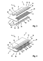
- FIG. 3 shows the off FIG. 1 known circuit board assembly without the plug in a 3D exploded view.
- Clearly visible are arranged in the portion 24 of the circuit board 2 printed conductors 8, which may be formed as contact pads. These interconnects 8 are usually connected electrically conductive with electrical components not shown here.
- Both the first spring element 18 and the second spring element 20 each have a Z-shape 26 with a first leg member 28 facing the printed circuit board 4 and a second leg member 30 spaced from the printed circuit board 4, wherein the first leg member 28 and the second leg member 30 by means of a first stake element 32 are permanently connected to each other.
- the second leg member 30 is adapted to engage the plug 10 as in FIG FIG. 1 shown to exert a force F1, F2.
- the second leg member 30 has an S-shape 34 with a first bay 36 and a second bay 38.
- the second bay 38 is designed to be on the not shown here, but from FIG. 1 to press known connector housing 12.
- the second leg member 30 is non-detachably connected to the first web member 32.
- Both the first spring element 18 and the second spring element 20 are each made in one piece from a cold-rolled sheet of stainless steel.
- the force F1, F2 is arcuately introduced into the first web element 32, so that no high stresses arise within the material at the transition of the first web element 32 to the second leg element 30.
- the second leg member 30 has cuts 40, which extend up to the first bay 36.
- the second leg member 30 is divided into resilient spring blades 42.
- This resilient spring blades 42 a uniform force distribution of the forces F1, F2 is ensured over the entire length of the plug housing 10.
- the resilient spring blades 42 manufacturing tolerances, in particular of the plug 10 can be compensated.
- the first leg member 28 of the first Spring element 18 and the first leg member 28 of the second spring element 20 are in the present design example by means of clinching, also called toxins, rigidly connected to each other inextricably, wherein the circuit board 4 extends between the two first leg members 28 in the longitudinal direction L of the circuit board 4.
- the forces F1, F2 are based on the two first web elements 32 via the two first leg elements 28. Characterized in that the two first leg members 28 are rigidly connected to each other, the forces acting perpendicular to the circuit board 4 forces F1, F2 are not passed into the circuit board 4. Thus, the circuit board 4 takes only forces that occur along the longitudinal direction L. These are usually the forces needed to push the plug 10 into its predetermined position on the printed circuit board 4.
- the first spring element 18 and the second spring element 20 are the same, so that they can be manufactured in a common tool. Also, the first spring element 18 and the second spring element 20 with respect to the circuit board 4 are arranged mirror images of each other.
- FIG. 5 shows a further embodiment of the printed circuit board assembly 2.
- the second spring element 20 is configured essentially in an L-shape 44 with a third leg element 46 and a second web element which is non-detachably connected to the third leg element 46 48.
- the first web element 32 of the first spring element 18 and the second web element 48 of the second spring element 20 are non-releasably rigidly connected to each other.
- the two web elements 32, 48 have centrally a common slot 52, which is present at a first end 56 and at a first end 56 opposite the second end 58 in each case by a web 54.
- the slot 52 is designed such that the portion 24 of the circuit board 4 can be threaded through the slot 52. This is done along the arrow 62. Furthermore, the circuit board 4 has adjacent to the portion 24 each have a recess 60 into which the two webs 54 can be inserted.
- the forces acting perpendicular to the longitudinal direction L of the circuit board 4 in connection with the plug 10 forces F1, F2 are received within the interconnected spring elements 18, 20, so that dispenses with an additional component for receiving the forces F1, F2 can be. Since the joining force increases along the longitudinal extension direction L of the printed circuit board 4 upon contact of the spring elements 18, 20 with the plug 10, a powerless insertion of the plug 10 on the printed circuit board 4 can take place.
- the spring elements 18, 20 may be configured continuously instead of the comb-like configuration.
Landscapes
- Coupling Device And Connection With Printed Circuit (AREA)
- Structures For Mounting Electric Components On Printed Circuit Boards (AREA)
- Multi-Conductor Connections (AREA)
Applications Claiming Priority (1)
| Application Number | Priority Date | Filing Date | Title |
|---|---|---|---|
| DE201210203297 DE102012203297A1 (de) | 2012-03-02 | 2012-03-02 | Leiterplattenvorrichtung und eine diesbezügliche elektrische Anordnung |
Publications (3)
| Publication Number | Publication Date |
|---|---|
| EP2634864A2 true EP2634864A2 (fr) | 2013-09-04 |
| EP2634864A3 EP2634864A3 (fr) | 2014-05-21 |
| EP2634864B1 EP2634864B1 (fr) | 2016-12-14 |
Family
ID=47632871
Family Applications (1)
| Application Number | Title | Priority Date | Filing Date |
|---|---|---|---|
| EP13153090.9A Not-in-force EP2634864B1 (fr) | 2012-03-02 | 2013-01-29 | Dispositif à plaquettes et agencement électrique correspondant |
Country Status (2)
| Country | Link |
|---|---|
| EP (1) | EP2634864B1 (fr) |
| DE (1) | DE102012203297A1 (fr) |
Families Citing this family (1)
| Publication number | Priority date | Publication date | Assignee | Title |
|---|---|---|---|---|
| DE102013214714A1 (de) * | 2013-07-29 | 2015-01-29 | Robert Bosch Gmbh | Steuergerät und Anordnung mit einem Steuergerät |
Family Cites Families (5)
| Publication number | Priority date | Publication date | Assignee | Title |
|---|---|---|---|---|
| US3639888A (en) * | 1970-01-15 | 1972-02-01 | Ind Electronic Hardware Corp | Printed circuit board connector |
| EP0036933A3 (fr) * | 1980-03-28 | 1981-12-02 | Bohdan Ulrich | Connecteur enfichable et son application à l'établissement d'une connexion électrique déconnectable |
| US5295852A (en) * | 1993-07-12 | 1994-03-22 | The Whitaker Corporation | Coplanar computer docking system |
| EP1009068A1 (fr) * | 1998-10-16 | 2000-06-14 | Molex Incorporated | Connecteur de bord pour circuits plats |
| US7413469B2 (en) * | 2005-10-11 | 2008-08-19 | Tyco Electronics Corporation | Electrical connector |
-
2012
- 2012-03-02 DE DE201210203297 patent/DE102012203297A1/de not_active Withdrawn
-
2013
- 2013-01-29 EP EP13153090.9A patent/EP2634864B1/fr not_active Not-in-force
Non-Patent Citations (1)
| Title |
|---|
| None |
Also Published As
| Publication number | Publication date |
|---|---|
| EP2634864B1 (fr) | 2016-12-14 |
| DE102012203297A1 (de) | 2013-09-05 |
| EP2634864A3 (fr) | 2014-05-21 |
Similar Documents
| Publication | Publication Date | Title |
|---|---|---|
| DE19607548C2 (de) | Abgewinkelter Einpreß-Steckverbinder zum Einpressen in Bohrungen einer Leiterplatte | |
| DE102009045550B4 (de) | Anschluss | |
| EP3446366B1 (fr) | Contact enfichable | |
| DE102008030101A1 (de) | Lötanschlusselement | |
| EP3000153A1 (fr) | Cavalier enfichable comprenant des éléments en tôle superposés | |
| DE102011119842A1 (de) | Elektrisches Verbindungselement und Leiterplattenanordnung | |
| DE102016108825B4 (de) | Klemmanordnung und Anschlussklemme | |
| WO2005107019A1 (fr) | Broche pour liaison electrique sans etain comprenant une plaque conductrice, outil d'estampage et procede pour produire une liaison electrique sans etain | |
| DE102009019699A1 (de) | Anschlussklemme für Leiterplatten | |
| EP1109259A2 (fr) | Connecteur électrique pour carte de circuit imprimé | |
| AT504960B1 (de) | Anordnung eines ersten schaltungsträgers auf einem zweiten schaltungsträger | |
| DE202008014542U1 (de) | Steckverbinder für Schaltungsplatinen | |
| DE102012218433B4 (de) | Kontaktanordnung | |
| EP2732508B1 (fr) | Elemnent connecteur directe avec verrouillage | |
| EP2689496B1 (fr) | Élément d'enfichage direct, en particulier pour appareils de commande de véhicule | |
| DE102010008354A1 (de) | Elektrische Anschlussklemme | |
| EP2634864B1 (fr) | Dispositif à plaquettes et agencement électrique correspondant | |
| DE202005014070U1 (de) | Leiterplatten-Einpressadapter | |
| DE102024108924A1 (de) | Durchlauferhitzer und Heizplatte für einen Durchlauferhitzer | |
| DE2140453C3 (de) | Kontaktfeder für Steckverbinder | |
| LU101643B1 (de) | Steckkontaktelement, Direktsteckverbinder, Verfahren zur Herstellung eines Steckkontaktelementes und Verfahren zur Herstellung eines Direktsteckverbinders | |
| EP1162694B1 (fr) | Appareil pour la connexion de conducteurs électriques | |
| DE19539958B4 (de) | Kontakt | |
| EP4128440A1 (fr) | Broche de contact par pression axialement élastique | |
| DE4136031C1 (en) | Double plug contact for car electric installation - consists of 2 terminal contact fins integral with strip conductor web |
Legal Events
| Date | Code | Title | Description |
|---|---|---|---|
| PUAI | Public reference made under article 153(3) epc to a published international application that has entered the european phase |
Free format text: ORIGINAL CODE: 0009012 |
|
| AK | Designated contracting states |
Kind code of ref document: A2 Designated state(s): AL AT BE BG CH CY CZ DE DK EE ES FI FR GB GR HR HU IE IS IT LI LT LU LV MC MK MT NL NO PL PT RO RS SE SI SK SM TR |
|
| AX | Request for extension of the european patent |
Extension state: BA ME |
|
| PUAL | Search report despatched |
Free format text: ORIGINAL CODE: 0009013 |
|
| AK | Designated contracting states |
Kind code of ref document: A3 Designated state(s): AL AT BE BG CH CY CZ DE DK EE ES FI FR GB GR HR HU IE IS IT LI LT LU LV MC MK MT NL NO PL PT RO RS SE SI SK SM TR |
|
| AX | Request for extension of the european patent |
Extension state: BA ME |
|
| RIC1 | Information provided on ipc code assigned before grant |
Ipc: H01R 12/72 20110101AFI20140414BHEP Ipc: H01R 12/85 20110101ALI20140414BHEP |
|
| 17P | Request for examination filed |
Effective date: 20141121 |
|
| RBV | Designated contracting states (corrected) |
Designated state(s): AL AT BE BG CH CY CZ DE DK EE ES FI FR GB GR HR HU IE IS IT LI LT LU LV MC MK MT NL NO PL PT RO RS SE SI SK SM TR |
|
| 17Q | First examination report despatched |
Effective date: 20151113 |
|
| GRAP | Despatch of communication of intention to grant a patent |
Free format text: ORIGINAL CODE: EPIDOSNIGR1 |
|
| INTG | Intention to grant announced |
Effective date: 20160628 |
|
| GRAJ | Information related to disapproval of communication of intention to grant by the applicant or resumption of examination proceedings by the epo deleted |
Free format text: ORIGINAL CODE: EPIDOSDIGR1 |
|
| GRAP | Despatch of communication of intention to grant a patent |
Free format text: ORIGINAL CODE: EPIDOSNIGR1 |
|
| INTC | Intention to grant announced (deleted) | ||
| INTG | Intention to grant announced |
Effective date: 20160914 |
|
| GRAS | Grant fee paid |
Free format text: ORIGINAL CODE: EPIDOSNIGR3 |
|
| GRAA | (expected) grant |
Free format text: ORIGINAL CODE: 0009210 |
|
| AK | Designated contracting states |
Kind code of ref document: B1 Designated state(s): AL AT BE BG CH CY CZ DE DK EE ES FI FR GB GR HR HU IE IS IT LI LT LU LV MC MK MT NL NO PL PT RO RS SE SI SK SM TR |
|
| REG | Reference to a national code |
Ref country code: GB Ref legal event code: FG4D Free format text: NOT ENGLISH |
|
| REG | Reference to a national code |
Ref country code: CH Ref legal event code: EP |
|
| REG | Reference to a national code |
Ref country code: IE Ref legal event code: FG4D Free format text: LANGUAGE OF EP DOCUMENT: GERMAN |
|
| REG | Reference to a national code |
Ref country code: AT Ref legal event code: REF Ref document number: 854344 Country of ref document: AT Kind code of ref document: T Effective date: 20170115 |
|
| REG | Reference to a national code |
Ref country code: DE Ref legal event code: R096 Ref document number: 502013005706 Country of ref document: DE |
|
| REG | Reference to a national code |
Ref country code: FR Ref legal event code: PLFP Year of fee payment: 5 |
|
| PG25 | Lapsed in a contracting state [announced via postgrant information from national office to epo] |
Ref country code: LV Free format text: LAPSE BECAUSE OF FAILURE TO SUBMIT A TRANSLATION OF THE DESCRIPTION OR TO PAY THE FEE WITHIN THE PRESCRIBED TIME-LIMIT Effective date: 20161214 |
|
| REG | Reference to a national code |
Ref country code: LT Ref legal event code: MG4D |
|
| REG | Reference to a national code |
Ref country code: NL Ref legal event code: MP Effective date: 20161214 |
|
| PG25 | Lapsed in a contracting state [announced via postgrant information from national office to epo] |
Ref country code: LT Free format text: LAPSE BECAUSE OF FAILURE TO SUBMIT A TRANSLATION OF THE DESCRIPTION OR TO PAY THE FEE WITHIN THE PRESCRIBED TIME-LIMIT Effective date: 20161214 Ref country code: NO Free format text: LAPSE BECAUSE OF FAILURE TO SUBMIT A TRANSLATION OF THE DESCRIPTION OR TO PAY THE FEE WITHIN THE PRESCRIBED TIME-LIMIT Effective date: 20170314 Ref country code: GR Free format text: LAPSE BECAUSE OF FAILURE TO SUBMIT A TRANSLATION OF THE DESCRIPTION OR TO PAY THE FEE WITHIN THE PRESCRIBED TIME-LIMIT Effective date: 20170315 Ref country code: SE Free format text: LAPSE BECAUSE OF FAILURE TO SUBMIT A TRANSLATION OF THE DESCRIPTION OR TO PAY THE FEE WITHIN THE PRESCRIBED TIME-LIMIT Effective date: 20161214 |
|
| PG25 | Lapsed in a contracting state [announced via postgrant information from national office to epo] |
Ref country code: RS Free format text: LAPSE BECAUSE OF FAILURE TO SUBMIT A TRANSLATION OF THE DESCRIPTION OR TO PAY THE FEE WITHIN THE PRESCRIBED TIME-LIMIT Effective date: 20161214 Ref country code: HR Free format text: LAPSE BECAUSE OF FAILURE TO SUBMIT A TRANSLATION OF THE DESCRIPTION OR TO PAY THE FEE WITHIN THE PRESCRIBED TIME-LIMIT Effective date: 20161214 Ref country code: BE Free format text: LAPSE BECAUSE OF NON-PAYMENT OF DUE FEES Effective date: 20170131 Ref country code: FI Free format text: LAPSE BECAUSE OF FAILURE TO SUBMIT A TRANSLATION OF THE DESCRIPTION OR TO PAY THE FEE WITHIN THE PRESCRIBED TIME-LIMIT Effective date: 20161214 |
|
| PG25 | Lapsed in a contracting state [announced via postgrant information from national office to epo] |
Ref country code: NL Free format text: LAPSE BECAUSE OF FAILURE TO SUBMIT A TRANSLATION OF THE DESCRIPTION OR TO PAY THE FEE WITHIN THE PRESCRIBED TIME-LIMIT Effective date: 20161214 |
|
| PG25 | Lapsed in a contracting state [announced via postgrant information from national office to epo] |
Ref country code: EE Free format text: LAPSE BECAUSE OF FAILURE TO SUBMIT A TRANSLATION OF THE DESCRIPTION OR TO PAY THE FEE WITHIN THE PRESCRIBED TIME-LIMIT Effective date: 20161214 Ref country code: RO Free format text: LAPSE BECAUSE OF FAILURE TO SUBMIT A TRANSLATION OF THE DESCRIPTION OR TO PAY THE FEE WITHIN THE PRESCRIBED TIME-LIMIT Effective date: 20161214 Ref country code: IS Free format text: LAPSE BECAUSE OF FAILURE TO SUBMIT A TRANSLATION OF THE DESCRIPTION OR TO PAY THE FEE WITHIN THE PRESCRIBED TIME-LIMIT Effective date: 20170414 Ref country code: SK Free format text: LAPSE BECAUSE OF FAILURE TO SUBMIT A TRANSLATION OF THE DESCRIPTION OR TO PAY THE FEE WITHIN THE PRESCRIBED TIME-LIMIT Effective date: 20161214 Ref country code: CZ Free format text: LAPSE BECAUSE OF FAILURE TO SUBMIT A TRANSLATION OF THE DESCRIPTION OR TO PAY THE FEE WITHIN THE PRESCRIBED TIME-LIMIT Effective date: 20161214 |
|
| PG25 | Lapsed in a contracting state [announced via postgrant information from national office to epo] |
Ref country code: PL Free format text: LAPSE BECAUSE OF FAILURE TO SUBMIT A TRANSLATION OF THE DESCRIPTION OR TO PAY THE FEE WITHIN THE PRESCRIBED TIME-LIMIT Effective date: 20161214 Ref country code: BG Free format text: LAPSE BECAUSE OF FAILURE TO SUBMIT A TRANSLATION OF THE DESCRIPTION OR TO PAY THE FEE WITHIN THE PRESCRIBED TIME-LIMIT Effective date: 20170314 Ref country code: SM Free format text: LAPSE BECAUSE OF FAILURE TO SUBMIT A TRANSLATION OF THE DESCRIPTION OR TO PAY THE FEE WITHIN THE PRESCRIBED TIME-LIMIT Effective date: 20161214 Ref country code: ES Free format text: LAPSE BECAUSE OF FAILURE TO SUBMIT A TRANSLATION OF THE DESCRIPTION OR TO PAY THE FEE WITHIN THE PRESCRIBED TIME-LIMIT Effective date: 20161214 Ref country code: PT Free format text: LAPSE BECAUSE OF FAILURE TO SUBMIT A TRANSLATION OF THE DESCRIPTION OR TO PAY THE FEE WITHIN THE PRESCRIBED TIME-LIMIT Effective date: 20170414 |
|
| REG | Reference to a national code |
Ref country code: CH Ref legal event code: PL |
|
| REG | Reference to a national code |
Ref country code: DE Ref legal event code: R097 Ref document number: 502013005706 Country of ref document: DE |
|
| PG25 | Lapsed in a contracting state [announced via postgrant information from national office to epo] |
Ref country code: MC Free format text: LAPSE BECAUSE OF FAILURE TO SUBMIT A TRANSLATION OF THE DESCRIPTION OR TO PAY THE FEE WITHIN THE PRESCRIBED TIME-LIMIT Effective date: 20161214 |
|
| PLBE | No opposition filed within time limit |
Free format text: ORIGINAL CODE: 0009261 |
|
| STAA | Information on the status of an ep patent application or granted ep patent |
Free format text: STATUS: NO OPPOSITION FILED WITHIN TIME LIMIT |
|
| PG25 | Lapsed in a contracting state [announced via postgrant information from national office to epo] |
Ref country code: LI Free format text: LAPSE BECAUSE OF NON-PAYMENT OF DUE FEES Effective date: 20170131 Ref country code: CH Free format text: LAPSE BECAUSE OF NON-PAYMENT OF DUE FEES Effective date: 20170131 |
|
| REG | Reference to a national code |
Ref country code: IE Ref legal event code: MM4A |
|
| 26N | No opposition filed |
Effective date: 20170915 |
|
| PG25 | Lapsed in a contracting state [announced via postgrant information from national office to epo] |
Ref country code: DK Free format text: LAPSE BECAUSE OF FAILURE TO SUBMIT A TRANSLATION OF THE DESCRIPTION OR TO PAY THE FEE WITHIN THE PRESCRIBED TIME-LIMIT Effective date: 20161214 Ref country code: LU Free format text: LAPSE BECAUSE OF NON-PAYMENT OF DUE FEES Effective date: 20170129 |
|
| REG | Reference to a national code |
Ref country code: FR Ref legal event code: PLFP Year of fee payment: 6 |
|
| REG | Reference to a national code |
Ref country code: BE Ref legal event code: MM Effective date: 20170131 |
|
| PG25 | Lapsed in a contracting state [announced via postgrant information from national office to epo] |
Ref country code: IE Free format text: LAPSE BECAUSE OF NON-PAYMENT OF DUE FEES Effective date: 20170129 Ref country code: SI Free format text: LAPSE BECAUSE OF FAILURE TO SUBMIT A TRANSLATION OF THE DESCRIPTION OR TO PAY THE FEE WITHIN THE PRESCRIBED TIME-LIMIT Effective date: 20161214 |
|
| PG25 | Lapsed in a contracting state [announced via postgrant information from national office to epo] |
Ref country code: MT Free format text: LAPSE BECAUSE OF FAILURE TO SUBMIT A TRANSLATION OF THE DESCRIPTION OR TO PAY THE FEE WITHIN THE PRESCRIBED TIME-LIMIT Effective date: 20161214 |
|
| REG | Reference to a national code |
Ref country code: AT Ref legal event code: MM01 Ref document number: 854344 Country of ref document: AT Kind code of ref document: T Effective date: 20180129 |
|
| PG25 | Lapsed in a contracting state [announced via postgrant information from national office to epo] |
Ref country code: AT Free format text: LAPSE BECAUSE OF NON-PAYMENT OF DUE FEES Effective date: 20180129 |
|
| PGFP | Annual fee paid to national office [announced via postgrant information from national office to epo] |
Ref country code: SE Payment date: 20190311 Year of fee payment: 8 |
|
| PG25 | Lapsed in a contracting state [announced via postgrant information from national office to epo] |
Ref country code: HU Free format text: LAPSE BECAUSE OF FAILURE TO SUBMIT A TRANSLATION OF THE DESCRIPTION OR TO PAY THE FEE WITHIN THE PRESCRIBED TIME-LIMIT; INVALID AB INITIO Effective date: 20130129 |
|
| PG25 | Lapsed in a contracting state [announced via postgrant information from national office to epo] |
Ref country code: CY Free format text: LAPSE BECAUSE OF NON-PAYMENT OF DUE FEES Effective date: 20161214 |
|
| PG25 | Lapsed in a contracting state [announced via postgrant information from national office to epo] |
Ref country code: MK Free format text: LAPSE BECAUSE OF FAILURE TO SUBMIT A TRANSLATION OF THE DESCRIPTION OR TO PAY THE FEE WITHIN THE PRESCRIBED TIME-LIMIT Effective date: 20161214 |
|
| PG25 | Lapsed in a contracting state [announced via postgrant information from national office to epo] |
Ref country code: TR Free format text: LAPSE BECAUSE OF FAILURE TO SUBMIT A TRANSLATION OF THE DESCRIPTION OR TO PAY THE FEE WITHIN THE PRESCRIBED TIME-LIMIT Effective date: 20161214 |
|
| PG25 | Lapsed in a contracting state [announced via postgrant information from national office to epo] |
Ref country code: AL Free format text: LAPSE BECAUSE OF FAILURE TO SUBMIT A TRANSLATION OF THE DESCRIPTION OR TO PAY THE FEE WITHIN THE PRESCRIBED TIME-LIMIT Effective date: 20161214 |
|
| GBPC | Gb: european patent ceased through non-payment of renewal fee |
Effective date: 20200129 |
|
| PG25 | Lapsed in a contracting state [announced via postgrant information from national office to epo] |
Ref country code: GB Free format text: LAPSE BECAUSE OF NON-PAYMENT OF DUE FEES Effective date: 20200129 Ref country code: FR Free format text: LAPSE BECAUSE OF NON-PAYMENT OF DUE FEES Effective date: 20200131 |
|
| PGFP | Annual fee paid to national office [announced via postgrant information from national office to epo] |
Ref country code: IT Payment date: 20210129 Year of fee payment: 9 |
|
| PGFP | Annual fee paid to national office [announced via postgrant information from national office to epo] |
Ref country code: DE Payment date: 20220324 Year of fee payment: 10 |
|
| PG25 | Lapsed in a contracting state [announced via postgrant information from national office to epo] |
Ref country code: IT Free format text: LAPSE BECAUSE OF NON-PAYMENT OF DUE FEES Effective date: 20220129 |
|
| REG | Reference to a national code |
Ref country code: DE Ref legal event code: R119 Ref document number: 502013005706 Country of ref document: DE |
|
| PG25 | Lapsed in a contracting state [announced via postgrant information from national office to epo] |
Ref country code: DE Free format text: LAPSE BECAUSE OF NON-PAYMENT OF DUE FEES Effective date: 20230801 |