EP2635722B1 - Procédé et dispositif de revêtement de substrats en continu - Google Patents
Procédé et dispositif de revêtement de substrats en continu Download PDFInfo
- Publication number
- EP2635722B1 EP2635722B1 EP11779621.9A EP11779621A EP2635722B1 EP 2635722 B1 EP2635722 B1 EP 2635722B1 EP 11779621 A EP11779621 A EP 11779621A EP 2635722 B1 EP2635722 B1 EP 2635722B1
- Authority
- EP
- European Patent Office
- Prior art keywords
- semiconductor material
- crucible
- lock
- substrate
- lock chamber
- Prior art date
- Legal status (The legal status is an assumption and is not a legal conclusion. Google has not performed a legal analysis and makes no representation as to the accuracy of the status listed.)
- Active
Links
Images
Classifications
-
- C—CHEMISTRY; METALLURGY
- C23—COATING METALLIC MATERIAL; COATING MATERIAL WITH METALLIC MATERIAL; CHEMICAL SURFACE TREATMENT; DIFFUSION TREATMENT OF METALLIC MATERIAL; COATING BY VACUUM EVAPORATION, BY SPUTTERING, BY ION IMPLANTATION OR BY CHEMICAL VAPOUR DEPOSITION, IN GENERAL; INHIBITING CORROSION OF METALLIC MATERIAL OR INCRUSTATION IN GENERAL
- C23C—COATING METALLIC MATERIAL; COATING MATERIAL WITH METALLIC MATERIAL; SURFACE TREATMENT OF METALLIC MATERIAL BY DIFFUSION INTO THE SURFACE, BY CHEMICAL CONVERSION OR SUBSTITUTION; COATING BY VACUUM EVAPORATION, BY SPUTTERING, BY ION IMPLANTATION OR BY CHEMICAL VAPOUR DEPOSITION, IN GENERAL
- C23C14/00—Coating by vacuum evaporation, by sputtering or by ion implantation of the coating forming material
- C23C14/22—Coating by vacuum evaporation, by sputtering or by ion implantation of the coating forming material characterised by the process of coating
- C23C14/24—Vacuum evaporation
- C23C14/246—Replenishment of source material
-
- H—ELECTRICITY
- H10—SEMICONDUCTOR DEVICES; ELECTRIC SOLID-STATE DEVICES NOT OTHERWISE PROVIDED FOR
- H10P—GENERIC PROCESSES OR APPARATUS FOR THE MANUFACTURE OR TREATMENT OF DEVICES COVERED BY CLASS H10
- H10P14/00—Formation of materials, e.g. in the shape of layers or pillars
- H10P14/20—Formation of materials, e.g. in the shape of layers or pillars of semiconductor materials
- H10P14/22—Formation of materials, e.g. in the shape of layers or pillars of semiconductor materials using physical deposition, e.g. vacuum deposition or sputtering
-
- C—CHEMISTRY; METALLURGY
- C23—COATING METALLIC MATERIAL; COATING MATERIAL WITH METALLIC MATERIAL; CHEMICAL SURFACE TREATMENT; DIFFUSION TREATMENT OF METALLIC MATERIAL; COATING BY VACUUM EVAPORATION, BY SPUTTERING, BY ION IMPLANTATION OR BY CHEMICAL VAPOUR DEPOSITION, IN GENERAL; INHIBITING CORROSION OF METALLIC MATERIAL OR INCRUSTATION IN GENERAL
- C23C—COATING METALLIC MATERIAL; COATING MATERIAL WITH METALLIC MATERIAL; SURFACE TREATMENT OF METALLIC MATERIAL BY DIFFUSION INTO THE SURFACE, BY CHEMICAL CONVERSION OR SUBSTITUTION; COATING BY VACUUM EVAPORATION, BY SPUTTERING, BY ION IMPLANTATION OR BY CHEMICAL VAPOUR DEPOSITION, IN GENERAL
- C23C14/00—Coating by vacuum evaporation, by sputtering or by ion implantation of the coating forming material
- C23C14/22—Coating by vacuum evaporation, by sputtering or by ion implantation of the coating forming material characterised by the process of coating
- C23C14/24—Vacuum evaporation
- C23C14/243—Crucibles for source material
-
- C—CHEMISTRY; METALLURGY
- C23—COATING METALLIC MATERIAL; COATING MATERIAL WITH METALLIC MATERIAL; CHEMICAL SURFACE TREATMENT; DIFFUSION TREATMENT OF METALLIC MATERIAL; COATING BY VACUUM EVAPORATION, BY SPUTTERING, BY ION IMPLANTATION OR BY CHEMICAL VAPOUR DEPOSITION, IN GENERAL; INHIBITING CORROSION OF METALLIC MATERIAL OR INCRUSTATION IN GENERAL
- C23C—COATING METALLIC MATERIAL; COATING MATERIAL WITH METALLIC MATERIAL; SURFACE TREATMENT OF METALLIC MATERIAL BY DIFFUSION INTO THE SURFACE, BY CHEMICAL CONVERSION OR SUBSTITUTION; COATING BY VACUUM EVAPORATION, BY SPUTTERING, BY ION IMPLANTATION OR BY CHEMICAL VAPOUR DEPOSITION, IN GENERAL
- C23C14/00—Coating by vacuum evaporation, by sputtering or by ion implantation of the coating forming material
- C23C14/22—Coating by vacuum evaporation, by sputtering or by ion implantation of the coating forming material characterised by the process of coating
- C23C14/56—Apparatus specially adapted for continuous coating; Arrangements for maintaining the vacuum, e.g. vacuum locks
- C23C14/564—Means for minimising impurities in the coating chamber such as dust, moisture, residual gases
- C23C14/566—Means for minimising impurities in the coating chamber such as dust, moisture, residual gases using a load-lock chamber
-
- H—ELECTRICITY
- H10—SEMICONDUCTOR DEVICES; ELECTRIC SOLID-STATE DEVICES NOT OTHERWISE PROVIDED FOR
- H10F—INORGANIC SEMICONDUCTOR DEVICES SENSITIVE TO INFRARED RADIATION, LIGHT, ELECTROMAGNETIC RADIATION OF SHORTER WAVELENGTH OR CORPUSCULAR RADIATION
- H10F71/00—Manufacture or treatment of devices covered by this subclass
- H10F71/125—The active layers comprising only Group II-VI materials, e.g. CdS, ZnS or CdTe
- H10F71/1257—The active layers comprising only Group II-VI materials, e.g. CdS, ZnS or CdTe comprising growth substrates not made of Group II-VI materials
-
- Y—GENERAL TAGGING OF NEW TECHNOLOGICAL DEVELOPMENTS; GENERAL TAGGING OF CROSS-SECTIONAL TECHNOLOGIES SPANNING OVER SEVERAL SECTIONS OF THE IPC; TECHNICAL SUBJECTS COVERED BY FORMER USPC CROSS-REFERENCE ART COLLECTIONS [XRACs] AND DIGESTS
- Y02—TECHNOLOGIES OR APPLICATIONS FOR MITIGATION OR ADAPTATION AGAINST CLIMATE CHANGE
- Y02E—REDUCTION OF GREENHOUSE GAS [GHG] EMISSIONS, RELATED TO ENERGY GENERATION, TRANSMISSION OR DISTRIBUTION
- Y02E10/00—Energy generation through renewable energy sources
- Y02E10/50—Photovoltaic [PV] energy
Definitions
- the invention relates to a method according to the preamble of claim 1 and a device suitable for this purpose. According to the method, a semiconductor material is vaporized in a crucible and guided to a surface of a substrate to be coated, where it is deposited.
- a substrate which is as transparent as possible usually a glass sheet, firstly with a TCO layer, that is an electrically conductive, transparent oxide layer, eg of zinc oxide (ZnO), tin oxide (SnO 2 ), indium oxide (In 2 O 2 ), Indium tin oxide also called ITO (mixture of ZnO and In 2 O 3 ) or cadmium stannate (CdSnO 4 ) coated.
- the TCO layer serves for contacting a cadmium sulfide layer (CdS layer) applied thereon.
- a CdTe layer is then applied to the CdS layer, to which a further conductive layer is then applied for contacting.
- the layers can also be applied in reverse order on a substrate and then covered with a transparent disc, such as a glass sheet.
- the individual layers are typically patterned to produce a plurality of photovoltaic cells connected in series on a glass sheet.
- a method of coating a substrate with a semiconductor is described.
- a semiconductor vapor-carrier gas mixture is introduced into a process chamber and directed against the substrate.
- a semiconductor powder is taken from a reservoir and transported with the carrier gas in a pipe system. During transport, the semiconductor powder is evaporated by supplying heat.
- DE 10 2010 061 259 A1 relates to a method for the deposition of CdTe.
- CdTe raw material is to be filled into a sublimation crucible without interrupting the coating process by means of locks which are not described in more detail
- the invention is based on the observation that the CSS reactor must be opened to provide semiconductor material, e.g. CdTe and / or CdS refill. This stops production, at least reducing CdTe pressure in the CSS reactor.
- semiconductor material e.g. CdTe and / or CdS refill.
- CdTe semiconductor material
- CdS refill e.g. CdS refill
- Adding CdTe to the crucible reduces the sublimation rate, resulting in uneven coating of the substrates. Because the reactor must be opened, toxic substances such as e.g. Cd or Te get into the area.
- the reactor is usually either evacuated or filled with an inert carrier gas. If the reactor is evacuated, it must be vented before opening. In particular, the subsequently necessary evacuation of the reactor prolongs the set-up time. If the reactor is filled with an inert carrier gas during the sublimation, this inert atmosphere must first be restored after filling the crucible, before the production can be resumed.
- the object of the invention is to reduce the quality fluctuations that arise when refilling semiconductor material into a crucible of a CSS reactor.
- EP 1970 474 A1 discloses an MBE device and a corresponding method for vapor deposition of CIS layers on a substrate.
- a molecular beam is directed through a slit-shaped aperture stop of an effusion cell onto a strip-shaped substrate.
- the aperture stop extends over the entire width of the substrate, so that a ribbon-shaped substrate can be vapor-deposited in its entire width while it is moved orthogonally to the longitudinal extent of the aperture stop.
- the width of the aperture stop increases to the edge of the same to apply a uniform layer as possible to the substrate.
- US 3,408,224 relates to a method of vaporizing a substrate with a metal layer.
- the metal to be evaporated is first melted under vacuum to degas it and then fed to a crucible through a system of communicating tubes.
- EP 0 337 369 A1 relates to the coating of non-metallic film layers with aluminum.
- the substrates are introduced continuously via upstream or downstream chambers with reduced pressure in the vapor deposition chamber.
- Aluminum is vaporized at the bottom of the vapor deposition chamber, which then condenses on the substrate guided over it. Evaporated aluminum is continuously replaced.
- EP 1 903 614 A2 describes a CSS method for depositing CdTe on top of about 1m 2 large glass panels and is therefore the closest prior art.
- the gist of the invention is semiconductor material, e.g. CdTe and / or CdS, in at least one crucible of a CSS reactor with continuous evaporation and preferably also continuous deposition of semiconductor material to a substrate to refill.
- semiconductor material e.g. CdTe and / or CdS
- an initial filling of the crucible can also be carried out by the method according to the invention.
- the process for continuously coating at least one substrate has at least the steps of evaporating at least one semiconductor material, e.g. CdTe, in at least one crucible and deposition of the semiconductor material on the substrate, wherein the crucible is filled during the evaporation and / or deposition with semiconductor material.
- the process is carried out in a sealed, in particular evacuated reactor, i. according to the CSS principle.
- semiconductor material such as CdS and / or CdTe
- this Prior to replenishment of semiconductor material, such as CdS and / or CdTe, this is preheated at least to +/- 20% of the temperature of the semiconductor material in the crucible, thereby fluctuations in the average temperature of the semiconductor material and thus the sublimation rate are reduced during refilling.
- the pressure in the CSS reactor and / or the average temperature of the semiconductor material in the crucible is kept at least approximately constant. This can be done, for example, by continuous filling of the crucible with semiconductor material, wherein the average temperature is kept constant by the heating of the crucible and / or by preheating the semiconductor material to be filled into the crucible.
- the semiconductor material to be replenished is heated to the temperature of the semiconductor material in the crucible, for example in a lock upstream of a CSS reactor, at least approximately ( ⁇ 20%, particularly preferably ⁇ 5%). If the semiconductor material to be replenished is introduced into the crucible by means of a lock is, in the lock, at least in a lock chamber, the atmosphere above the crucible, or in the CSS reactor preferably replicated. If the coating takes place, for example, in a vacuum, the air or another gas is preferably withdrawn from the lock and the semiconductor material introduced therein is heated therein. As a result, the atmosphere of the CSS reactor can be simulated in the lock.
- the lock may have several lock chambers, in which the steps are performed sequentially.
- material and semiconductor material herein refer to both the starting material and that on the substrate, e.g. a glass sheet, deposited material, which need not necessarily be identical.
- the crucible is typically heated.
- crucible and sublimation crucible are used as a synonym for a vessel suitable for the evaporation of material.
- the semiconductor material is introduced for filling the crucible in at least a first lock chamber.
- a lock chamber is a closable space arranged between at least one closable inlet opening and at least one closable outlet opening.
- the semiconductor material for filling the crucible in a CSS reactor can be introduced without the interior of the CSS reactor is connected directly to the outside world.
- one first opens the otherwise closed inlet opening of the lock chamber brings through this semiconductor material into the lock chamber, closes the inlet opening of the lock chamber again, then opens the otherwise closed outlet port of the lock chamber and transports the semiconductor material through the open outlet opening of the lock chamber from the lock chamber into the lock chamber Reactor.
- the atmosphere is reproduced in the CSS reactor and only then the outlet opening of the lock chamber opened.
- This can prevent the atmosphere in the CSS reactor being affected by gases contained in the lock chamber, ie the process in the CSS reactor is largely unaffected by gases in the lock chamber.
- semiconductor material for filling the crucible is introduced into the lock chamber through the inlet opening, wherein the outlet opening is closed. Subsequently, the inlet opening is closed and the atmosphere of the CSS reactor is replicated.
- the lock chamber is evacuated, ie a vacuum is generated.
- the outlet opening can be opened and the semiconductor material can be transported in the direction of the crucible.
- the term vacuum here does not stand for a theoretically evacuated space, but for a pressure that is less than the ambient pressure.
- the pressure level in the lock chamber after generating the vacuum at least approximately ( ⁇ 20% preferably ⁇ 5%) corresponds to the pressure level in the CSS reactor.
- the reactor is not evacuated, but is filled with an inert gas, eg, a noble gas or nitrogen (N 2 ).
- the step of replicating comprises introducing inert gas into the sluice gate.
- the lock chamber can be evacuated beforehand.
- the CSS reactor has a lower pressure than standard pressure, the residual pressure being at least substantially generated by an inert gas. This atmosphere is also preferably formed in the lock chamber before opening the outlet opening of the lock chamber.
- the semiconductor material is heated to refill the crucible in at least one lock chamber before it is filled into the crucible.
- temperature fluctuations in the crucible can be minimized by refilling semiconductor material into the crucible, and the sublimation process is not or only insignificantly influenced by the refilling of semiconductor material.
- the semiconductor material flow from the crucible to the substrate remains at least substantially constant.
- Deposition rate of the semiconductor material on the substrate at least substantially constant. A uniform layer growth on the substrate is the result.
- semiconductor material is introduced into the at least one first lock chamber and then an atmosphere is generated in the first lock chamber which corresponds at least approximately to the pressure of the atmosphere in the CSS reactor and a further lock chamber arranged between the first lock chamber and the reactor. If the reactor and the further lock chamber evacuated, then the first lock chamber is also evacuated. Subsequently, the semiconductor material is shipped into at least one other lock chamber. In the further lock chamber, the charged semiconductor material is preheated to at least approximately ( ⁇ 20%, preferably ⁇ 5% or better) the temperature of the semiconductor material in the crucible. The preheated semiconductor material is then filled into the crucible. Thus, neither the temperature in the crucible nor the atmosphere in the CSS reactor is significantly affected by the filling of the crucible.
- the sublimation rate and thus also the deposition rate of the semiconductor material on the substrate thus remain at least approximately constant.
- the process for depositing semiconductor material can be carried out continuously without significant quality fluctuations of the coated substrates occurring. Because the process of generating a negative pressure and heating the semiconductor material are performed in separate gates, these operations are necessarily performed sequentially. Thus, in the first lock, there is no sublimation of semiconductor material which could escape into the environment during later reopening of the inlet opening.
- the same partial pressure is generated for semiconductor material to be vaporized, as in the CSS reactor. This can especially be done by Heating the semiconductor material in the further lock under at least substantially similar or identical atmospheric conditions as done in the CSS reactor.
- the concentration of the gaseous semiconductor material in the CSS reactor is thus only negligibly impaired, if at all, ie the deposition rate of the semiconductor material on the substrate is not significantly affected by the opening of the outlet opening of the further lock.
- This method can be carried out in a particularly simple manner if the outlet opening of the first lock chamber is connected to the inlet opening of the further lock chamber and the outlet opening of the further lock chamber is simultaneously the inlet opening into the reactor.
- the first lock chamber above the further lock chamber and the further lock chamber can again be arranged above the reactor. Then it is sufficient to open the corresponding inlet and outlet openings and the semiconductor material slips or falls due to gravity of the first lock in the other lock and from there into the crucible.
- Semiconductor material is preferably transported by the first lock chamber into at least two further lock chambers, by which it is filled alternately into the crucible, thereby the supply of semiconductor material into the crucible becomes more continuous. Variations of the sublimation rate and thus also the deposition rate of the semiconductor material on the substrate are reduced.
- An apparatus for the continuous deposition of a semiconductor material on a substrate according to the CSS method has at least one closed CSS reactor in which at least one crucible for sublimating semiconductor material is arranged, and at least one receptacle for at least one substrate, which can be arranged on the receptacle such that previously sublimed semiconductor material is deposited on the substrate.
- the device also has at least one first lock with a first lock chamber arranged between at least one inlet opening and at least one outlet opening for holding semiconductor material and preferably also means for evacuating the lock.
- the device preferably has at least one further lock chamber or lock with a further lock chamber arranged between an inlet opening and an outlet opening and means for heating semiconductor material introduced into the further lock.
- the further lock or lock chamber is preferably arranged between the first lock and the reactor.
- the pressure in the further lock chamber preferably corresponds at least approximately to the pressure in the interior of the reactor.
- outlet port of the first port is located above the inlet port of the further port, then semiconductor material may be gravity-fed from the first port to the further port by simply opening the respective inlet and outlet ports, respectively.
- the outlet opening of the first lock and the inlet opening of the other lock can be identical. In the arrangement of the outlet or inlet opening, it should only be ensured that the semiconductor material is transported by gravity from one into the further lock, for example falls or slips when the outlet or inlet opening is opened.
- the outlet opening is arranged for this purpose, preferably at the deepest part of the one lock, otherwise the semiconductor material must be actively conveyed to the outlet opening, for example by a conveying means such as a vibrating conveyor.
- the outlet opening of the further lock is arranged above the crucible, then falls and / or slides when opening the outlet opening of the other lock previously shipped there semiconductor material in the crucible.
- the outlet opening is accordingly arranged, preferably at the lowest area of the further lock.
- the outlet opening of the further lock can be arranged above a storage container, from where the semiconductor material is filled in small portions into the crucible. More preferably, the semiconductor material is continuously, e.g. by a corresponding conveying means such as e.g. a vibrating conveyor or a screw transported in the crucible.
- a corresponding conveying means such as e.g. a vibrating conveyor or a screw transported in the crucible.
- the semiconductor material is distributed in the crucible.
- the surface of the semiconductor material can be kept at least approximately constant at and / or after each filling of the crucible.
- the evaporation rate and thus also the deposition rate is made even more uniform.
- the crucible may e.g. be shaken.
- it preferably has means for shaking.
- the crucible is preferably arranged in a CSS reactor above and / or next to the substrate, thereby semiconductor material can be easily refilled from above.
- a channel is preferably attached, the end facing away from the crucible ends open down above the substrate.
- the channel is preferably arranged together with the crucible in an oven. If the channel is additionally heated, it is avoided that it gets clogged over time. Therefore, the temperature of the channel wall is preferably greater than the temperature of the semiconductor material in the crucible.
- substrates have often been coated from below.
- the invention has the advantage that in the described coating of the substrate from above the substrate can be supported on its underside over a large area or at least at closely adjacent locations. As a result, a sagging of the substrates otherwise supported only in the edge region is prevented and the process temperature can be increased, which leads to improved efficiency, for example, in CdTe thin-film solar modules.
- At least one grating is preferably arranged in its end section in order to uniform the flow velocity of the gaseous semiconductor material in the direction of the substrate over the channel cross section.
- the grid is preferably heated, which can be prevented that it is added to semiconductor material.
- the temperature of the grid should be greater than or equal to the temperature of the material in the crucible.
- the grating may be a conductive plate having a plurality of holes.
- the CSS reactor has at least one closable opening through which semiconductor material can be filled into the crucible.
- the closable opening may e.g. be placed in the wall of the channel or in the crucible wall, it should be above the maximum filling height of the crucible. Then, semiconductor material introduced through the opening drops into the crucible, thus filling the crucible.
- the closable opening is preferably an outlet opening of a lock and / or a lock arrangement comprising at least two locks.
- the CSS reactor has means for distributing semiconductor material in the crucible, eg, means for shaking the crucible.
- a cone is formed. Through the cone is the material surface, ie the surface of the semiconductor material at this evaporates, larger than before filling. Accordingly, the evaporation rate increases. As the evaporation rate increases, so does the deposition rate of the semiconductor material on the substrate. If after refilling the semiconductor material is evenly distributed in the crucible, for example by shaking the crucible, fluctuations of the material surface and thus also the deposition rate can be minimized.
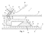
- Fig. 1 shows a sketch of a CSS reactor for sublimation of semiconductor material, for example cadmium telluride (CdTe) and / or cadmium sulfate (CdS) and desublimation of the semiconductor material on a substrate in section.
- semiconductor material for example cadmium telluride (CdTe) and / or cadmium sulfate (CdS) and desublimation of the semiconductor material on a substrate in section.
- the CSS reactor 1 is a module of a production line for thin-film solar modules. It is suitable for coating substrates 14, e.g. Glass sheets with a semiconductor material, e.g. CdTe.
- the CSS reactor 1 has a channel-like housing and can be connected on both sides with other modules of the manufacturing line.
- a guide on the substrates such as 14 can be moved through the CSS reactor 1 (indicated by arrow 13).
- the guide has a plurality of rollers 12 on which the substrate 14 rests. At least some of the rollers 12 are driven.
- a heated crucible 30 is disposed above the guide in the housing.
- the crucible merges seamlessly into a likewise heated channel 20, whose open end facing away from the crucible 21, ie its opening 21 facing away from the crucible, is as possible is arranged just above the substrate 14.
- the end portion 23 above the substrate 14 is widened in a funnel shape. In the end portion 23, two grids 22 are arranged.
- a lock arrangement comprising a first lock 40 and a further lock 50.
- the first lock is arranged at least partially outside the housing.
- the further lock is preferably arranged at least partially within the heated housing 10.
- the first lock has a lock chamber 44.
- In the lock chamber 44 opens a closable vacuum line 48 for connecting the lock chamber 44 to a vacuum pump (not shown).
- a closable vacuum line 48 for connecting the lock chamber 44 to a vacuum pump (not shown).
- At the upper end of the lock chamber 44 is an inlet opening 41 and at the lower end of the lock chamber 44 is an outlet opening 45.
- the inlet opening 41 is closed by a shutter 42 shown schematically as a flap.
- the outlet opening 45 can also be closed by means of a closure 46 which is shown schematically as a flap.
- the further lock 50 has at its upper end an inlet opening 51 which is closed by the closure 46.
- a closable outlet opening 55 is arranged above the crucible 30.
- the semiconductor material 16 in the crucible 30 is evaporated. Accordingly, at least the crucible and the channel are heated. At least the inlet opening 41 of the first lock chamber 44 is through the closure 42 locked. Preferably, at least the outlet opening 45 of the first lock chamber 44 is closed.
- the gaseous semiconductor material is distributed in the channel.
- the grids 22 serve to unify the flow velocity of the gaseous semiconductor material 16 over the channel cross-section. As a result, the semiconductor material is deposited more uniformly than without grid 22 on the substrate.
- the grids are heated so that as little as possible semiconductor material attaches to you, which would lead to a blockage of the grating 22.
- the heating may be indirect as well as direct, e.g. by passing a current through the grids 22.
- the grids are preferably convexly curved. As a result, the flow velocity of the gaseous semiconductor material is also substantially homogeneous in the widened end section 23.
- the funnel-shaped extension of the end portion 23 has the advantage that the semiconductor material is locally relatively slow, i. is deposited at a low growth rate. This improves the efficiency of the later thin-film solar modules. At the same time, however, it is deposited over a large area, so that the necessary layer thickness of the semiconductor layer is nevertheless achieved fairly quickly, i. the cycle rate of the production line is increased.
- the supply in the crucible 30 is consumed.
- the outlet opening 45 of the first lock chamber 40 is closed and the inlet opening 41 of the first lock chamber 40 is opened.
- the inlet opening 41 is closed again.
- the first lock chamber 44 is evacuated via the vacuum line 48.
- the outlet opening 55 of the further lock chamber 54 is closed and then the inlet opening 51 of the further lock 50 is opened and the outlet opening 41 of the first lock 40 is opened.
- the semiconductor material 16 is transported into the further lock chamber.
- both lock chambers 44, 54 could now be vented via the vacuum line 48.
- the inlet opening 41 of the further lock 40 is closed again and the semiconductor material 16 is heated in the further lock chamber to a temperature which corresponds at least approximately to the temperature of the semiconductor material in the crucible.
- the outlet opening 55 of the further lock 50 can be opened, whereby the semiconductor material from the further lock 50 is filled into the crucible 30.
- semiconductor material 16 While the semiconductor material 16 is heated in the further lock 50, semiconductor material 16 can again be introduced into the first lock 40 and subsequently a vacuum can again be generated in the first lock 40.
- new semiconductor material 16 can be loaded from the first lock 40 into the further lock 50. This allows a higher timing when filling the crucible 30. Accordingly, with the same total amount of semiconductor material 16 which is refilled into the crucible 30, the individual quantities which are filled with each opening of the outlet port 55 of the other lock 50 into the crucible 30, thus reducing the evaporation rate in the crucible 30 is less affected.
- the lock arrangement comprising at least one first lock 40 and at least one further lock 50, semiconductor material can be replenished into the crucible 30 during deposition.
- semiconductor material can be replenished into the crucible 30 during deposition. The necessary according to the prior art, stopping the production line for refilling of semiconductor material can thus be omitted.
Landscapes
- Chemical & Material Sciences (AREA)
- Chemical Kinetics & Catalysis (AREA)
- Engineering & Computer Science (AREA)
- Materials Engineering (AREA)
- Mechanical Engineering (AREA)
- Metallurgy (AREA)
- Organic Chemistry (AREA)
- Physical Vapour Deposition (AREA)
- Photovoltaic Devices (AREA)
- Physical Deposition Of Substances That Are Components Of Semiconductor Devices (AREA)
Claims (15)
- Procédé pour le revêtement en continu d'au moins un substrat (14) dans un réacteur de sublimation CSS, comprenant au moins les étapes de :- évaporation d'au moins un matériau semi-conducteur (16) dans au moins un creuset (30) et- dépôt du matériau semi-conducteur (16) par le haut sur le substrat,caractérisé en ce que le creuset (30) est rempli de matériau semi-conducteur (16) pendant le dépôt et/ou l'évaporation et le matériau semi-conducteur est préchauffé, avant d'être amené au creuset, au moins jusqu'à ±20 % de sa température dans le creuset.
- Procédé selon la revendication 1, caractérisé en ce que le matériau semi-conducteur (16) pour le remplissage du creuset (30) est amené dans au moins une première chambre de sas (44).
- Procédé selon la revendication 2, caractérisé en ce qu'après l'introduction du matériau semi-conducteur (16), un vide est créé dans la première chambre de sas (44).
- Procédé selon la revendication 2 ou 3, caractérisé en ce que le matériau semi-conducteur (16) pour le remplissage du creuset (30) est chauffé dans au moins une chambre de sas (54) avant d'être amené dans le creuset (30).
- Procédé selon les revendications 2, 3 et 4, caractérisé en ce que- du matériau semi-conducteur (16) est introduit dans l'au moins une première chambre de sas (44) et un vide est ensuite créé dans la première chambre de sas (44),- le matériau semi-conducteur (16) est ensuite transporté dans au moins une autre chambre de sas (54),- le matériau semi-conducteur (16) est ensuite chauffé dans l'autre chambre de sas (54) et- le creuset (30) est rempli avec le matériau semi-conducteur (16) chauffé.
- Procédé selon la revendication 5, caractérisé en ce que le matériau semi-conducteur (16) est transporté de la première chambre de sas (44) vers au moins deux autres chambres de sas (54), à partir desquelles il est amené alternativement dans le creuset (30).
- Réacteur de sublimation CSS (1) pour l'évaporation d'au moins un matériau semi-conducteur (16) avec au moins un creuset (30) au-dessus d'au moins un guidage pour au moins un substrat, caractérisé en ce que le réacteur de sublimation CSS (1) possède au moins un premier sas (40) avec une chambre de sas (44) disposée entre au moins une ouverture d'entrée (41) et au moins une ouverture de sortie (45) pour emmagasiner du matériau semi-conducteur (16), des moyens pour faire le vide dans le sas (40), des moyens pour chauffer le matériau semi-conducteur jusqu'à au moins ±20 % de sa température dans le creuset et des moyens pour transporter du matériau semi-conducteur du sas vers le creuset.
- Réacteur de sublimation CSS (1) selon la revendication 7, caractérisé en ce que le réacteur de sublimation CSS (1) possède au moins un autre sas (50) avec une autre chambre de sas (54) disposée entre au moins une ouverture d'entrée (51) et au moins une ouverture de sortie (55) et des moyens pour chauffer du matériau semi-conducteur (16) introduit dans l'autre sas (50).
- Dispositif selon la revendication 8, caractérisé en ce que l'autre sas (50) est disposé entre l'au moins un premier sas (40) et le creuset (30).
- Dispositif selon la revendication 9, caractérisé en ce que l'ouverture de sortie (46) du premier sas (40) est disposée au-dessus de l'ouverture d'entrée (51) de l'autre sas (50).
- Dispositif selon l'une des revendications 9 ou 10, caractérisé en ce que l'ouverture de sortie (56) de l'autre sas (50) est disposée au-dessus du creuset (30).
- Dispositif selon l'une des revendications 7 à 11, caractérisé en ce que l'ouverture d'entrée (41) du premier sas (40) communique avec l'ouverture de sortie d'un réservoir (60).
- Dispositif selon l'une des revendications 7 à 12, caractérisé en ce qu'il est prévu au-dessus du creuset (30) une ouverture d'un canal (20) qui présente une extrémité ouverte au-dessus du guidage afin d'amener du matériau semi-conducteur (16) évaporé par le canal (20) du creuset (30) vers la face supérieure d'au moins un substrat (14) retenu sur le guidage.
- Dispositif selon la revendication 13, caractérisé en ce qu'au moins une grille (22) est disposée dans le canal (20) ou au moins à une de ses extrémités.
- Dispositif selon l'une des revendications 7 à 14, caractérisé en ce que le guidage comprend au moins un élément de support (12) pour un substrat (14), lequel élément de support (12) présente au moins un appui pour le substrat (14) disposé entre les bords latéraux du substrat (14), afin d'au moins réduire une inflexion du substrat (14).
Applications Claiming Priority (2)
| Application Number | Priority Date | Filing Date | Title |
|---|---|---|---|
| DE102010060292.2A DE102010060292B4 (de) | 2010-11-01 | 2010-11-01 | Verfahren und CSS-Reaktor zum kontinuierlichen Beschichten von Substraten |
| PCT/EP2011/069056 WO2012059439A1 (fr) | 2010-11-01 | 2011-10-28 | Procédé et dispositif de revêtement de substrats en continu |
Publications (2)
| Publication Number | Publication Date |
|---|---|
| EP2635722A1 EP2635722A1 (fr) | 2013-09-11 |
| EP2635722B1 true EP2635722B1 (fr) | 2015-04-08 |
Family
ID=44913263
Family Applications (1)
| Application Number | Title | Priority Date | Filing Date |
|---|---|---|---|
| EP11779621.9A Active EP2635722B1 (fr) | 2010-11-01 | 2011-10-28 | Procédé et dispositif de revêtement de substrats en continu |
Country Status (4)
| Country | Link |
|---|---|
| US (1) | US9343305B2 (fr) |
| EP (1) | EP2635722B1 (fr) |
| DE (1) | DE102010060292B4 (fr) |
| WO (1) | WO2012059439A1 (fr) |
Families Citing this family (5)
| Publication number | Priority date | Publication date | Assignee | Title |
|---|---|---|---|---|
| WO2012083018A1 (fr) * | 2010-12-17 | 2012-06-21 | First Solar, Inc. | Dispositif photovoltaïque |
| CN111934645B (zh) * | 2020-08-13 | 2023-03-24 | 厦门市三安集成电路有限公司 | 铝铜合金膜层的制备方法、声表面波滤波器以及双工器 |
| DE102021006288A1 (de) | 2021-12-21 | 2023-06-22 | Singulus Technologies Aktiengesellschaft | Beschichtungsquelle mit Nachfüllvorrichtung |
| CN120035687A (zh) * | 2022-07-01 | 2025-05-23 | 中国建材国际工程集团有限公司 | 涂层材料蒸发装置及其用途 |
| CN117660887A (zh) * | 2022-08-25 | 2024-03-08 | 中国建材国际工程集团有限公司 | 用于蒸发系统的自上而下的升华装置及其用途 |
Citations (1)
| Publication number | Priority date | Publication date | Assignee | Title |
|---|---|---|---|---|
| DE102010061259A1 (de) * | 2009-12-15 | 2011-06-16 | PrimeStar Solar, Inc., Arvada | Modulares System und Verfahren zur kontinuierlichen Abscheidung einer dünnen Filmschicht auf einem Substrat |
Family Cites Families (11)
| Publication number | Priority date | Publication date | Assignee | Title |
|---|---|---|---|---|
| US3408224A (en) | 1964-06-25 | 1968-10-29 | Pennsalt Chemicals Corp | Vapor coating employing degassing of coating metal |
| KR920003591B1 (ko) | 1988-04-11 | 1992-05-04 | 미쯔비시주우고오교오 가부시기가이샤 | 연속진공증착장치 |
| US5248349A (en) | 1992-05-12 | 1993-09-28 | Solar Cells, Inc. | Process for making photovoltaic devices and resultant product |
| US7014702B2 (en) * | 2000-05-31 | 2006-03-21 | Pirelli Cavi E Sistemi S.P.A. | Method and apparatus for preparation of binary and higher order compounds and devices fabricated using same |
| US6551405B1 (en) | 2000-09-22 | 2003-04-22 | The Board Of Trustees Of The University Of Arkansas | Tool and method for in situ vapor phase deposition source material reloading and maintenance |
| US7927659B2 (en) * | 2005-04-26 | 2011-04-19 | First Solar, Inc. | System and method for depositing a material on a substrate |
| DE102007012370A1 (de) * | 2007-03-14 | 2008-09-18 | Createc Fischer & Co. Gmbh | Bedampfungseinrichtung und Bedampfungsverfahren zur Molekularstrahlbedampfung und Molekularstrahlepitaxie |
| DE202008009492U1 (de) * | 2008-07-15 | 2009-11-26 | Tallinn University Of Technology | Halbleitermaterial und dessen Verwendung als Absorptionsmaterial für Solarzellen |
| JP2010144221A (ja) * | 2008-12-18 | 2010-07-01 | Tokyo Electron Ltd | 原料ガス発生装置及び成膜装置 |
| DE102009009022A1 (de) * | 2009-02-16 | 2010-08-26 | Centrotherm Photovoltaics Ag | Verfahren und Vorrichtung zur Beschichtung von flachen Substraten mit Chalkogenen |
| US8252117B2 (en) * | 2010-01-07 | 2012-08-28 | Primestar Solar, Inc. | Automatic feed system and related process for introducing source material to a thin film vapor deposition system |
-
2010
- 2010-11-01 DE DE102010060292.2A patent/DE102010060292B4/de active Active
-
2011
- 2011-10-28 WO PCT/EP2011/069056 patent/WO2012059439A1/fr not_active Ceased
- 2011-10-28 EP EP11779621.9A patent/EP2635722B1/fr active Active
- 2011-10-28 US US13/993,410 patent/US9343305B2/en active Active
Patent Citations (1)
| Publication number | Priority date | Publication date | Assignee | Title |
|---|---|---|---|---|
| DE102010061259A1 (de) * | 2009-12-15 | 2011-06-16 | PrimeStar Solar, Inc., Arvada | Modulares System und Verfahren zur kontinuierlichen Abscheidung einer dünnen Filmschicht auf einem Substrat |
Also Published As
| Publication number | Publication date |
|---|---|
| EP2635722A1 (fr) | 2013-09-11 |
| DE102010060292B4 (de) | 2023-05-25 |
| WO2012059439A1 (fr) | 2012-05-10 |
| DE102010060292A1 (de) | 2012-05-03 |
| US20140147992A1 (en) | 2014-05-29 |
| US9343305B2 (en) | 2016-05-17 |
Similar Documents
| Publication | Publication Date | Title |
|---|---|---|
| DE102010061631A1 (de) | Automatisches Zuführsystem und zugehöriges Verfahren zur Zuführung von Ausgangsmaterial zu einer Dünnschicht-Dampfphasenabscheidungsvorrichtung | |
| EP2144296B2 (fr) | Procédé de fabrication d'une couche semi-conductrice | |
| WO2010060646A1 (fr) | Procédé de fabrication de couches semi-conductrices ou de substrats revêtus, traités par du sélénium et/ou du soufre élémentaire, en particulier de substrats bidimensionnels | |
| DE102010061259B4 (de) | Modulares System und Verfahren zur kontinuierlichen Abscheidung einer dünnen Filmschicht auf einem Substrat | |
| EP2635722B1 (fr) | Procédé et dispositif de revêtement de substrats en continu | |
| KR20100052429A (ko) | 칼코겐을 제공하기 위한 방법 및 장치 | |
| DE102011056913A1 (de) | Dampfabscheidungsverfahren zur kontinuierlichen Abscheidung und Behandlung einer Dünnfilmschicht auf einem Substrat | |
| DE60211470T2 (de) | Vorrichtung und Verfahren zur Herstellung von flexiblen Halbleiter-Einrichtungen | |
| EP2870625B1 (fr) | Installation et procédé destinés à traiter des substrats | |
| DE102011056645A1 (de) | Dampfabscheidungsvorrichtung und Verfahren zur kontinuierlichen Abscheidung einer dotierten Dünnfilmschicht auf einem Substrat | |
| DE102011056911A1 (de) | Integrierte Abscheidung von Dünnfilmschichten bei der Herstellung von Photovoltaikmodulen auf Basis von Cadmiumtellurid | |
| DE102017208289A1 (de) | Schichterzeugungsverfahren | |
| DE69615598T2 (de) | Erzeugung des Magnesiumdampfes mit hocher Verdampfungsgeschwindigkeit | |
| EP1558782B1 (fr) | Dispositif et procede de depot en phase vapeur sous vide d'un supraconducteur à haute température avec remplissage de matériau automatique | |
| DE102010061223B4 (de) | Dampfphasenabscheidevorrichtung zur kontinuierlichen Abscheidung einer dünnen Filmschicht auf einem Substrat | |
| EP2553136B1 (fr) | Procédé de remplissage d'une chambre d'évaporateur | |
| DE102011056906A1 (de) | Dampfabscheidungsvorrichtung und Verfahren zur kontinuierlichen Abscheidung einer Dünnfilmschicht auf einem Substrat | |
| DE102009011496A1 (de) | Verfahren und Vorrichtung zur thermischen Umsetzung metallischer Precursorschichten in halbleitende Schichten mit Chalkogenrückgewinnung | |
| DE102009009022A1 (de) | Verfahren und Vorrichtung zur Beschichtung von flachen Substraten mit Chalkogenen | |
| DE102011056907B4 (de) | Zeitlich variable Abscheidungsrate von CdTe in einer Vorrichtung und einem Verfahren zur kontinuierlichen Abscheidung | |
| EP2371991B1 (fr) | Procédé de remplissage discontinu d'une chambre d'évaporateur de sélénium | |
| DE102012022744B4 (de) | Vorrichtung zum Einstellen einer Gasphase in einer Reaktionskammer | |
| EP2369034B1 (fr) | Procédé de remplissage d'une chambre d'évaporateur de sélénium | |
| DE4442733C2 (de) | Einrichtung zur Bedampfung bandförmiger Substrate im Vakuum | |
| DE102009012200A1 (de) | Verfahren und Vorrichtung zur thermischen Umsetzung metallischer Precursorschichten in halbleitende Schichten mit Chalkogenquelle |
Legal Events
| Date | Code | Title | Description |
|---|---|---|---|
| PUAI | Public reference made under article 153(3) epc to a published international application that has entered the european phase |
Free format text: ORIGINAL CODE: 0009012 |
|
| 17P | Request for examination filed |
Effective date: 20130603 |
|
| AK | Designated contracting states |
Kind code of ref document: A1 Designated state(s): AL AT BE BG CH CY CZ DE DK EE ES FI FR GB GR HR HU IE IS IT LI LT LU LV MC MK MT NL NO PL PT RO RS SE SI SK SM TR |
|
| DAX | Request for extension of the european patent (deleted) | ||
| 17Q | First examination report despatched |
Effective date: 20140404 |
|
| REG | Reference to a national code |
Ref country code: DE Ref legal event code: R079 Ref document number: 502011006549 Country of ref document: DE Free format text: PREVIOUS MAIN CLASS: C23C0014240000 Ipc: H01L0031180000 |
|
| GRAP | Despatch of communication of intention to grant a patent |
Free format text: ORIGINAL CODE: EPIDOSNIGR1 |
|
| RIC1 | Information provided on ipc code assigned before grant |
Ipc: H01L 31/18 20060101AFI20140916BHEP |
|
| INTG | Intention to grant announced |
Effective date: 20141020 |
|
| GRAS | Grant fee paid |
Free format text: ORIGINAL CODE: EPIDOSNIGR3 |
|
| GRAA | (expected) grant |
Free format text: ORIGINAL CODE: 0009210 |
|
| AK | Designated contracting states |
Kind code of ref document: B1 Designated state(s): AL AT BE BG CH CY CZ DE DK EE ES FI FR GB GR HR HU IE IS IT LI LT LU LV MC MK MT NL NO PL PT RO RS SE SI SK SM TR |
|
| REG | Reference to a national code |
Ref country code: GB Ref legal event code: FG4D Free format text: NOT ENGLISH |
|
| REG | Reference to a national code |
Ref country code: CH Ref legal event code: EP |
|
| REG | Reference to a national code |
Ref country code: IE Ref legal event code: FG4D Free format text: LANGUAGE OF EP DOCUMENT: GERMAN |
|
| REG | Reference to a national code |
Ref country code: AT Ref legal event code: REF Ref document number: 721124 Country of ref document: AT Kind code of ref document: T Effective date: 20150515 |
|
| REG | Reference to a national code |
Ref country code: DE Ref legal event code: R096 Ref document number: 502011006549 Country of ref document: DE Effective date: 20150521 |
|
| REG | Reference to a national code |
Ref country code: NL Ref legal event code: VDEP Effective date: 20150408 |
|
| REG | Reference to a national code |
Ref country code: LT Ref legal event code: MG4D |
|
| PG25 | Lapsed in a contracting state [announced via postgrant information from national office to epo] |
Ref country code: NL Free format text: LAPSE BECAUSE OF FAILURE TO SUBMIT A TRANSLATION OF THE DESCRIPTION OR TO PAY THE FEE WITHIN THE PRESCRIBED TIME-LIMIT Effective date: 20150408 |
|
| PG25 | Lapsed in a contracting state [announced via postgrant information from national office to epo] |
Ref country code: PT Free format text: LAPSE BECAUSE OF FAILURE TO SUBMIT A TRANSLATION OF THE DESCRIPTION OR TO PAY THE FEE WITHIN THE PRESCRIBED TIME-LIMIT Effective date: 20150810 Ref country code: ES Free format text: LAPSE BECAUSE OF FAILURE TO SUBMIT A TRANSLATION OF THE DESCRIPTION OR TO PAY THE FEE WITHIN THE PRESCRIBED TIME-LIMIT Effective date: 20150408 Ref country code: HR Free format text: LAPSE BECAUSE OF FAILURE TO SUBMIT A TRANSLATION OF THE DESCRIPTION OR TO PAY THE FEE WITHIN THE PRESCRIBED TIME-LIMIT Effective date: 20150408 Ref country code: LT Free format text: LAPSE BECAUSE OF FAILURE TO SUBMIT A TRANSLATION OF THE DESCRIPTION OR TO PAY THE FEE WITHIN THE PRESCRIBED TIME-LIMIT Effective date: 20150408 Ref country code: FI Free format text: LAPSE BECAUSE OF FAILURE TO SUBMIT A TRANSLATION OF THE DESCRIPTION OR TO PAY THE FEE WITHIN THE PRESCRIBED TIME-LIMIT Effective date: 20150408 Ref country code: NO Free format text: LAPSE BECAUSE OF FAILURE TO SUBMIT A TRANSLATION OF THE DESCRIPTION OR TO PAY THE FEE WITHIN THE PRESCRIBED TIME-LIMIT Effective date: 20150708 |
|
| PG25 | Lapsed in a contracting state [announced via postgrant information from national office to epo] |
Ref country code: IS Free format text: LAPSE BECAUSE OF FAILURE TO SUBMIT A TRANSLATION OF THE DESCRIPTION OR TO PAY THE FEE WITHIN THE PRESCRIBED TIME-LIMIT Effective date: 20150808 Ref country code: GR Free format text: LAPSE BECAUSE OF FAILURE TO SUBMIT A TRANSLATION OF THE DESCRIPTION OR TO PAY THE FEE WITHIN THE PRESCRIBED TIME-LIMIT Effective date: 20150709 Ref country code: RS Free format text: LAPSE BECAUSE OF FAILURE TO SUBMIT A TRANSLATION OF THE DESCRIPTION OR TO PAY THE FEE WITHIN THE PRESCRIBED TIME-LIMIT Effective date: 20150408 Ref country code: LV Free format text: LAPSE BECAUSE OF FAILURE TO SUBMIT A TRANSLATION OF THE DESCRIPTION OR TO PAY THE FEE WITHIN THE PRESCRIBED TIME-LIMIT Effective date: 20150408 |
|
| REG | Reference to a national code |
Ref country code: DE Ref legal event code: R097 Ref document number: 502011006549 Country of ref document: DE |
|
| PG25 | Lapsed in a contracting state [announced via postgrant information from national office to epo] |
Ref country code: DK Free format text: LAPSE BECAUSE OF FAILURE TO SUBMIT A TRANSLATION OF THE DESCRIPTION OR TO PAY THE FEE WITHIN THE PRESCRIBED TIME-LIMIT Effective date: 20150408 Ref country code: EE Free format text: LAPSE BECAUSE OF FAILURE TO SUBMIT A TRANSLATION OF THE DESCRIPTION OR TO PAY THE FEE WITHIN THE PRESCRIBED TIME-LIMIT Effective date: 20150408 |
|
| PLBE | No opposition filed within time limit |
Free format text: ORIGINAL CODE: 0009261 |
|
| STAA | Information on the status of an ep patent application or granted ep patent |
Free format text: STATUS: NO OPPOSITION FILED WITHIN TIME LIMIT |
|
| PG25 | Lapsed in a contracting state [announced via postgrant information from national office to epo] |
Ref country code: PL Free format text: LAPSE BECAUSE OF FAILURE TO SUBMIT A TRANSLATION OF THE DESCRIPTION OR TO PAY THE FEE WITHIN THE PRESCRIBED TIME-LIMIT Effective date: 20150408 Ref country code: CZ Free format text: LAPSE BECAUSE OF FAILURE TO SUBMIT A TRANSLATION OF THE DESCRIPTION OR TO PAY THE FEE WITHIN THE PRESCRIBED TIME-LIMIT Effective date: 20150408 Ref country code: RO Free format text: LAPSE BECAUSE OF NON-PAYMENT OF DUE FEES Effective date: 20150408 Ref country code: SK Free format text: LAPSE BECAUSE OF FAILURE TO SUBMIT A TRANSLATION OF THE DESCRIPTION OR TO PAY THE FEE WITHIN THE PRESCRIBED TIME-LIMIT Effective date: 20150408 |
|
| 26N | No opposition filed |
Effective date: 20160111 |
|
| PG25 | Lapsed in a contracting state [announced via postgrant information from national office to epo] |
Ref country code: IT Free format text: LAPSE BECAUSE OF FAILURE TO SUBMIT A TRANSLATION OF THE DESCRIPTION OR TO PAY THE FEE WITHIN THE PRESCRIBED TIME-LIMIT Effective date: 20150408 |
|
| PG25 | Lapsed in a contracting state [announced via postgrant information from national office to epo] |
Ref country code: SI Free format text: LAPSE BECAUSE OF FAILURE TO SUBMIT A TRANSLATION OF THE DESCRIPTION OR TO PAY THE FEE WITHIN THE PRESCRIBED TIME-LIMIT Effective date: 20150408 Ref country code: LU Free format text: LAPSE BECAUSE OF FAILURE TO SUBMIT A TRANSLATION OF THE DESCRIPTION OR TO PAY THE FEE WITHIN THE PRESCRIBED TIME-LIMIT Effective date: 20151028 |
|
| GBPC | Gb: european patent ceased through non-payment of renewal fee |
Effective date: 20151028 |
|
| PG25 | Lapsed in a contracting state [announced via postgrant information from national office to epo] |
Ref country code: MC Free format text: LAPSE BECAUSE OF FAILURE TO SUBMIT A TRANSLATION OF THE DESCRIPTION OR TO PAY THE FEE WITHIN THE PRESCRIBED TIME-LIMIT Effective date: 20150408 |
|
| REG | Reference to a national code |
Ref country code: IE Ref legal event code: MM4A |
|
| PG25 | Lapsed in a contracting state [announced via postgrant information from national office to epo] |
Ref country code: GB Free format text: LAPSE BECAUSE OF NON-PAYMENT OF DUE FEES Effective date: 20151028 |
|
| REG | Reference to a national code |
Ref country code: FR Ref legal event code: ST Effective date: 20160630 |
|
| PG25 | Lapsed in a contracting state [announced via postgrant information from national office to epo] |
Ref country code: FR Free format text: LAPSE BECAUSE OF NON-PAYMENT OF DUE FEES Effective date: 20151102 |
|
| PG25 | Lapsed in a contracting state [announced via postgrant information from national office to epo] |
Ref country code: IE Free format text: LAPSE BECAUSE OF NON-PAYMENT OF DUE FEES Effective date: 20151028 |
|
| PG25 | Lapsed in a contracting state [announced via postgrant information from national office to epo] |
Ref country code: BG Free format text: LAPSE BECAUSE OF FAILURE TO SUBMIT A TRANSLATION OF THE DESCRIPTION OR TO PAY THE FEE WITHIN THE PRESCRIBED TIME-LIMIT Effective date: 20150408 Ref country code: SM Free format text: LAPSE BECAUSE OF FAILURE TO SUBMIT A TRANSLATION OF THE DESCRIPTION OR TO PAY THE FEE WITHIN THE PRESCRIBED TIME-LIMIT Effective date: 20150408 Ref country code: HU Free format text: LAPSE BECAUSE OF FAILURE TO SUBMIT A TRANSLATION OF THE DESCRIPTION OR TO PAY THE FEE WITHIN THE PRESCRIBED TIME-LIMIT; INVALID AB INITIO Effective date: 20111028 |
|
| PG25 | Lapsed in a contracting state [announced via postgrant information from national office to epo] |
Ref country code: CY Free format text: LAPSE BECAUSE OF FAILURE TO SUBMIT A TRANSLATION OF THE DESCRIPTION OR TO PAY THE FEE WITHIN THE PRESCRIBED TIME-LIMIT Effective date: 20150408 Ref country code: SE Free format text: LAPSE BECAUSE OF FAILURE TO SUBMIT A TRANSLATION OF THE DESCRIPTION OR TO PAY THE FEE WITHIN THE PRESCRIBED TIME-LIMIT Effective date: 20150408 |
|
| PG25 | Lapsed in a contracting state [announced via postgrant information from national office to epo] |
Ref country code: BE Free format text: LAPSE BECAUSE OF NON-PAYMENT OF DUE FEES Effective date: 20151031 |
|
| PG25 | Lapsed in a contracting state [announced via postgrant information from national office to epo] |
Ref country code: MT Free format text: LAPSE BECAUSE OF FAILURE TO SUBMIT A TRANSLATION OF THE DESCRIPTION OR TO PAY THE FEE WITHIN THE PRESCRIBED TIME-LIMIT Effective date: 20150408 |
|
| REG | Reference to a national code |
Ref country code: AT Ref legal event code: MM01 Ref document number: 721124 Country of ref document: AT Kind code of ref document: T Effective date: 20161028 |
|
| PG25 | Lapsed in a contracting state [announced via postgrant information from national office to epo] |
Ref country code: AT Free format text: LAPSE BECAUSE OF NON-PAYMENT OF DUE FEES Effective date: 20161028 |
|
| PG25 | Lapsed in a contracting state [announced via postgrant information from national office to epo] |
Ref country code: TR Free format text: LAPSE BECAUSE OF FAILURE TO SUBMIT A TRANSLATION OF THE DESCRIPTION OR TO PAY THE FEE WITHIN THE PRESCRIBED TIME-LIMIT Effective date: 20150408 Ref country code: MK Free format text: LAPSE BECAUSE OF FAILURE TO SUBMIT A TRANSLATION OF THE DESCRIPTION OR TO PAY THE FEE WITHIN THE PRESCRIBED TIME-LIMIT Effective date: 20150408 |
|
| PG25 | Lapsed in a contracting state [announced via postgrant information from national office to epo] |
Ref country code: AL Free format text: LAPSE BECAUSE OF FAILURE TO SUBMIT A TRANSLATION OF THE DESCRIPTION OR TO PAY THE FEE WITHIN THE PRESCRIBED TIME-LIMIT Effective date: 20150408 |
|
| REG | Reference to a national code |
Ref country code: DE Ref legal event code: R079 Ref document number: 502011006549 Country of ref document: DE Free format text: PREVIOUS MAIN CLASS: H01L0031180000 Ipc: H10F0071000000 |
|
| REG | Reference to a national code |
Ref country code: CH Ref legal event code: U11 Free format text: ST27 STATUS EVENT CODE: U-0-0-U10-U11 (AS PROVIDED BY THE NATIONAL OFFICE) Effective date: 20251101 |
|
| PGFP | Annual fee paid to national office [announced via postgrant information from national office to epo] |
Ref country code: DE Payment date: 20251027 Year of fee payment: 15 |
|
| PGFP | Annual fee paid to national office [announced via postgrant information from national office to epo] |
Ref country code: CH Payment date: 20251101 Year of fee payment: 15 |