EP2636718A2 - Dispositif électroluminescent blanc - Google Patents
Dispositif électroluminescent blanc Download PDFInfo
- Publication number
- EP2636718A2 EP2636718A2 EP13156044.3A EP13156044A EP2636718A2 EP 2636718 A2 EP2636718 A2 EP 2636718A2 EP 13156044 A EP13156044 A EP 13156044A EP 2636718 A2 EP2636718 A2 EP 2636718A2
- Authority
- EP
- European Patent Office
- Prior art keywords
- peak wavelength
- fluorescent material
- light emitting
- fluorescent
- emitting element
- Prior art date
- Legal status (The legal status is an assumption and is not a legal conclusion. Google has not performed a legal analysis and makes no representation as to the accuracy of the status listed.)
- Granted
Links
Images


Classifications
-
- H—ELECTRICITY
- H05—ELECTRIC TECHNIQUES NOT OTHERWISE PROVIDED FOR
- H05B—ELECTRIC HEATING; ELECTRIC LIGHT SOURCES NOT OTHERWISE PROVIDED FOR; CIRCUIT ARRANGEMENTS FOR ELECTRIC LIGHT SOURCES, IN GENERAL
- H05B33/00—Electroluminescent light sources
- H05B33/12—Light sources with substantially two-dimensional [2D] radiating surfaces
-
- H—ELECTRICITY
- H10—SEMICONDUCTOR DEVICES; ELECTRIC SOLID-STATE DEVICES NOT OTHERWISE PROVIDED FOR
- H10H—INORGANIC LIGHT-EMITTING SEMICONDUCTOR DEVICES HAVING POTENTIAL BARRIERS
- H10H20/00—Individual inorganic light-emitting semiconductor devices having potential barriers, e.g. light-emitting diodes [LED]
- H10H20/80—Constructional details
- H10H20/85—Packages
- H10H20/851—Wavelength conversion means
-
- C—CHEMISTRY; METALLURGY
- C09—DYES; PAINTS; POLISHES; NATURAL RESINS; ADHESIVES; COMPOSITIONS NOT OTHERWISE PROVIDED FOR; APPLICATIONS OF MATERIALS NOT OTHERWISE PROVIDED FOR
- C09K—MATERIALS FOR MISCELLANEOUS APPLICATIONS, NOT PROVIDED FOR ELSEWHERE
- C09K11/00—Luminescent materials, e.g. electroluminescent or chemiluminescent
- C09K11/08—Luminescent materials, e.g. electroluminescent or chemiluminescent containing inorganic luminescent materials
- C09K11/77—Luminescent materials, e.g. electroluminescent or chemiluminescent containing inorganic luminescent materials containing rare earth metals
- C09K11/7728—Luminescent materials, e.g. electroluminescent or chemiluminescent containing inorganic luminescent materials containing rare earth metals containing europium
- C09K11/77347—Silicon Nitrides or Silicon Oxynitrides
-
- C—CHEMISTRY; METALLURGY
- C09—DYES; PAINTS; POLISHES; NATURAL RESINS; ADHESIVES; COMPOSITIONS NOT OTHERWISE PROVIDED FOR; APPLICATIONS OF MATERIALS NOT OTHERWISE PROVIDED FOR
- C09K—MATERIALS FOR MISCELLANEOUS APPLICATIONS, NOT PROVIDED FOR ELSEWHERE
- C09K11/00—Luminescent materials, e.g. electroluminescent or chemiluminescent
- C09K11/08—Luminescent materials, e.g. electroluminescent or chemiluminescent containing inorganic luminescent materials
- C09K11/77—Luminescent materials, e.g. electroluminescent or chemiluminescent containing inorganic luminescent materials containing rare earth metals
- C09K11/7728—Luminescent materials, e.g. electroluminescent or chemiluminescent containing inorganic luminescent materials containing rare earth metals containing europium
- C09K11/77348—Silicon Aluminium Nitrides or Silicon Aluminium Oxynitrides
-
- H—ELECTRICITY
- H10—SEMICONDUCTOR DEVICES; ELECTRIC SOLID-STATE DEVICES NOT OTHERWISE PROVIDED FOR
- H10H—INORGANIC LIGHT-EMITTING SEMICONDUCTOR DEVICES HAVING POTENTIAL BARRIERS
- H10H20/00—Individual inorganic light-emitting semiconductor devices having potential barriers, e.g. light-emitting diodes [LED]
- H10H20/80—Constructional details
- H10H20/85—Packages
- H10H20/851—Wavelength conversion means
- H10H20/8511—Wavelength conversion means characterised by their material, e.g. binder
- H10H20/8512—Wavelength conversion materials
- H10H20/8513—Wavelength conversion materials having two or more wavelength conversion materials
-
- H—ELECTRICITY
- H10—SEMICONDUCTOR DEVICES; ELECTRIC SOLID-STATE DEVICES NOT OTHERWISE PROVIDED FOR
- H10H—INORGANIC LIGHT-EMITTING SEMICONDUCTOR DEVICES HAVING POTENTIAL BARRIERS
- H10H20/00—Individual inorganic light-emitting semiconductor devices having potential barriers, e.g. light-emitting diodes [LED]
- H10H20/80—Constructional details
- H10H20/85—Packages
- H10H20/851—Wavelength conversion means
- H10H20/8515—Wavelength conversion means not being in contact with the bodies
-
- H—ELECTRICITY
- H10—SEMICONDUCTOR DEVICES; ELECTRIC SOLID-STATE DEVICES NOT OTHERWISE PROVIDED FOR
- H10W—GENERIC PACKAGES, INTERCONNECTIONS, CONNECTORS OR OTHER CONSTRUCTIONAL DETAILS OF DEVICES COVERED BY CLASS H10
- H10W72/00—Interconnections or connectors in packages
- H10W72/50—Bond wires
- H10W72/551—Materials of bond wires
- H10W72/552—Materials of bond wires comprising metals or metalloids, e.g. silver
- H10W72/5522—Materials of bond wires comprising metals or metalloids, e.g. silver comprising gold [Au]
-
- Y—GENERAL TAGGING OF NEW TECHNOLOGICAL DEVELOPMENTS; GENERAL TAGGING OF CROSS-SECTIONAL TECHNOLOGIES SPANNING OVER SEVERAL SECTIONS OF THE IPC; TECHNICAL SUBJECTS COVERED BY FORMER USPC CROSS-REFERENCE ART COLLECTIONS [XRACs] AND DIGESTS
- Y02—TECHNOLOGIES OR APPLICATIONS FOR MITIGATION OR ADAPTATION AGAINST CLIMATE CHANGE
- Y02B—CLIMATE CHANGE MITIGATION TECHNOLOGIES RELATED TO BUILDINGS, e.g. HOUSING, HOUSE APPLIANCES OR RELATED END-USER APPLICATIONS
- Y02B20/00—Energy efficient lighting technologies, e.g. halogen lamps or gas discharge lamps
Definitions
- Embodiments described herein relate generally to a white light emitting device.
- Light emitting devices using a light emitting diode are mainly composed of a combination of an LED chip as an excitation light source and a fluorescent material. Further, a variety of luminescent colors can be achieved depending on the combination.
- a combination of an LED chip for emitting blue light with a fluorescent material is used.
- a yellow fluorescent material is mainly used which emits light complementary to blue, and with the LED chip, used as a pseudo white light LED.
- three-wavelength white LEDs have been developed which use an LED chip for emitting blue light, a green to yellow fluorescent material, and a red fluorescent material.
- the white light emitting devices it is desirable for the white light emitting devices to achieve high color rendering properties, in particular, a high average color rendering index (Ra) in order to reproduce a color close to natural light.
- the devices require a balance with a high luminescent efficiency.
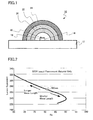
- FIG. 1 is a schematic cross-sectional view of a light emitting device according to a first embodiment
- FIG. 2 is a diagram showing a simulation result in the case of one kind of SION based fluorescent material
- FIG. 3 is a diagram showing an example of emission spectra obtained from a simulation
- FIGS. 4A and 4B are diagrams showing simulation results in the present embodiment
- FIG. 5 is a diagram for explaining the function and effect of the embodiment.
- FIG. 6 is a schematic cross-sectional view of a light emitting device according to a second embodiment.
- a white light emitting device includes: a light emitting element which has a peak wavelength in a wavelength range of 430 nm or more and 470 nm or less; a first fluorescent material which emits light with a first peak wavelength of 525 nm or more and 560 nm or less; a second fluorescent material which emits light with a second peak wavelength longer than the first peak wavelength; and a third fluorescent material which emits light with a third peak wavelength of 620 nm or more and 750 nm or less, which is longer than the second peak wavelength.
- first fluorescent material and the second fluorescent material have a composition of MSi ⁇ O ⁇ N ⁇ (However, M includes Eu, necessarily includes Sr or Ba, and may further include Ca, Mg, and Zn. Furthermore, M may contain, as an activator agent, element(s) selected from the group including Ti, Pb, Mn, As, Al, Pr, Tb, and Ce.
- ⁇ , ⁇ , and ⁇ satisfy 1.8 ⁇ ⁇ ⁇ 2.4, 1.8 ⁇ ⁇ 2.2, and 1.8 ⁇ ⁇ ⁇ 2.2.), and when the first peak wavelength is denoted by ⁇ 1 (nm), whereas the second peak wavelength is denoted by ⁇ 2 (nm), conditions of 1100 ⁇ ⁇ 1 + ⁇ 2 and ⁇ 2 - ⁇ 1 ⁇ 60 are satisfied.
- a white light emitting device includes: a light emitting element which has a peak wavelength in a wavelength range of 430 nm or more and 470 nm or less; a first fluorescent material which emits light with a first peak wavelength of 525 nm or more and 560 nm or less; a second fluorescent material which emits light with a second peak wavelength longer than the first peak wavelength; and a third fluorescent material which emits light with a third peak wavelength of 620 nm or more and 750 nm or less, which is longer than the second peak wavelength.
- first fluorescent material and the second fluorescent material have a composition of: MSi ⁇ O ⁇ N ⁇ (However, M includes Eu, necessarily includes Sr or Ba, and may further include Ca, Mg, and Zn. Furthermore, M may contain, as an activator agent, element(s) selected from the group including Ti, Pb, Mn, As, Al, Pr, Tb, and Ce.
- ⁇ , ⁇ , and ⁇ satisfy 1.8 ⁇ ⁇ ⁇ 2.4, 1.8 ⁇ ⁇ ⁇ 2.2, and 1.8 ⁇ ⁇ ⁇ 2.2.) when the first peak wavelength is denoted by ⁇ 1 (nm), whereas the second peak wavelength is denoted by ⁇ 2 (nm), conditions of 1100 ⁇ ⁇ 1 + ⁇ 2 and ⁇ 2 - ⁇ 1 ⁇ 60 are satisfied.
- the white light emitting device has the configuration described above, thereby making it possible to achieve high color rendering properties, in particular, a high average color rendering index Ra and a high luminescent efficiency. More specifically, the combination of, the light emitting element for emitting blue light, two kinds of yellow-green to orange fluorescent materials of the same host (or structure) which are different in peak wavelength, and the red fluorescent material makes it possible to achieve a balance between high color rendering properties and a high luminescent efficiency.
- FIG. 1 is a schematic cross-sectional view of a light emitting device according to the present embodiment.
- This light emitting device 10 is a white light emitting device which emits white light.
- the light emitting device 10 is a white light emitting device which has a luminescent color of a incandescent lamp color (2800 K).
- the white light emitting device 10 includes a substrate 12 which has a flat surface with a light emitting element to be mounted.
- a highly reflective material is used for the substrate 12.
- a blue LED chip for example, is mounted on the flat surface of the substrate 12.
- the blue LED chip is connected to a wiring, not shown, through, for example, a gold wire 16. Further, the external supply of a driving current through this wiring to the blue LED chip causes the blue LED chip to produce blue light for excitation.
- the blue LED chip is, for example, an AIGainN based LED which has GalnN as a light emitting layer.
- An element sealing transparent layer 18 composed of a hemispherically-shaped transparent resin is provided on the light emitting element 14.
- the transparent resin is, for example, a silicone resin.
- a first fluorescent layer 20 with a circumference semicircular in cross section perpendicular to the flat surface is formed so as to cover the element sealing transparent layer 18.
- the first fluorescent layer 20 contains therein a first fluorescent material which emits light with a first peak wavelength of 525 nm or more and 560 nm or less, with the use of light emitted from the light emitting element 14 as excitation light.
- the first fluorescent material (hereinafter, an abbreviation of Y1 also used) is a yellow-green to yellow fluorescent material.
- the first fluorescent layer 20 is formed by dispersing, for example, yellow-green to orange fluorescent material particles in, for example, a transparent silicone resin.
- the first fluorescent layer 20 absorbs blue light generated from the blue LED to convert the blue light to yellow-green to yellow light.
- a second fluorescent layer 22 with a circumference semicircular in cross section perpendicular to the flat surface is formed so as to cover the first fluorescent layer 20.
- the second fluorescent layer 22 contains therein a second fluorescent material which emits light with a second peak wavelength longer than the first peak wavelength, with the use of light emitted from the light emitting element 14 as excitation light.
- the second fluorescent material (hereinafter, an abbreviation of Y2 also used) is a yellow to orange fluorescent material.
- the second fluorescent layer 22 is formed by dispersing, for example, yellow to orange fluorescent material particles in, for example, a transparent silicone resin.
- the second fluorescent layer 22 absorbs blue light generated from the blue LED to convert the blue light to yellow to orange light.
- the first fluorescent material and the second fluorescent material are both socalled SION based fluorescent materials which have the following composition: MSi ⁇ O ⁇ N ⁇ (However, M represents two or more metals including europium (Eu), and necessarily includes strontium (Sr) or barium (Ba), and may further include calcium (Ca), magnesium (Mg), and zinc (Zn). Furthermore, M may contain, as an activator agent, element(s) selected from the group including titanium (Ti), lead (Pb), manganese (Mn), arsenic (As), aluminum (Al), praseodymium (Pr), terbium (Tb), and cerium (Ce). In addition, ⁇ , ⁇ , and ⁇ satisfy 1.8 ⁇ ⁇ ⁇ 2.4, 1.8 ⁇ ⁇ ⁇ 2.2, and 1.8 ⁇ ⁇ ⁇ 2.2.)
- ⁇ , ⁇ , and ⁇ satisfy 2.0 ⁇ ⁇ ⁇ 2.2, 1.8 ⁇ ⁇ ⁇ 2.1, and 1.9 ⁇ ⁇ ⁇ 2.2.
- the first fluorescent material and the second fluorescent material both have the following composition: (Sr (1-x-y-z) Ba x Ca y Eu z )Si 2 O 2 N 2 (in the formula, 0 ⁇ x ⁇ 1, 0 ⁇ y ⁇ 1, 0.01 ⁇ z ⁇ 0.2) It is possible to adjust the emission wavelength of the oxynitride fluorescent material containing Si, which is represented by this formula, by, for example, changing the composition in terms of x and y, and fluorescent materials can be obtained which have more than one emission wavelength in the same host.
- strontium (Sr), barium (Ba), and calcium (Ca) may be substituted for at least either one of Mg and Zn.
- at least one element selected from the group including Ti, Pb, Mn, As, Al, Pr, Tb, and Ce may be contained in minute amounts as an activator agent.
- the SION based fluorescent material has excellent temperature characteristics of changes in luminescent efficiency by approximately 10% or less at 25°C to 150°C. Therefore, it is possible to suppress color deviations in the white light emitting device during high-temperature operation.
- a third fluorescent layer 24 with a circumference semicircular in cross section perpendicular to the flat surface is formed so as to cover the second fluorescent layer 22.
- the third fluorescent layer 24 contains therein a third fluorescent material which emits light with a third peak wavelength of 620 nm or more and 750 nm or less, which is longer than the second peak wavelength, with the use of light emitted from the light emitting element 14 as excitation light.
- the third fluorescent material (hereinafter, an abbreviation of R also used) is a red fluorescent material.
- the third fluorescent layer 24 is formed by dispersing, for example, red fluorescent material particles in, for example, a transparent silicone resin.
- the third fluorescent layer 24 absorbs blue light generated from the blue LED to convert the blue light to red light.
- the third fluorescent material is, for example, Ca 2 Si y Al (12-y) O z N (16-z) :Eu, a socalled CASN-based fluorescent material.
- the luminescent efficiency the theoretical value of the luminescent efficiency, that is, the lumen equivalent (lumen/watt of emission) was used as an index, in order to ignore the efficiency of the light emitting element and the efficiencies of the fluorescent materials.
- the color rendering properties and luminescent efficiency were simulated for the combination of the blue light emitting element, one kind of SION based yellow-green to orange fluorescent material, and a red fluorescent material.
- a measured spectrum for a yellow fluorescent material with a peak wavelength of 563 nm was shifted and used as the spectrum for the yellow-green to orange fluorescent material.
- FIG. 2 is a diagram showing a simulation result in the case of SION based fluorescent material only. In this case only one kind of SION based fluorescent material is used.
- the horizontal axis indicates an average color rendering index Ra, whereas the vertical axis indicates a lumen equivalent (Im/W).
- the color rendering properties and luminescent efficiency were simulated for the combination of the blue light emitting element with two kinds of fluorescent materials different in peak wavelength, selected from yellow-green to orange SION based fluorescent materials.
- the fluorescent material with a peak wavelength on the shorter wavelength side is referred to as Y1
- the fluorescent material with a peak wavelength on the longer wavelength side is referred to as Y2.
- the respective peak wavelengths ⁇ 1 and ⁇ 2 of the fluorescent materials Y1 and Y2 were used as variables.
- the peak wavelength of Y1 was varied by 2 nm between 520 nm and 565 nm
- the peak wavelength of Y2 was varied by 2 nm from the peak wavelength of Y1 to a difference of 60 nm.
- the intensity ratio among Y1, Y2, and R was adjusted so that the chromaticity of the spectrum was adapted to a incandescent lamp color at 2800 K.
- the color rendering properties and luminescent efficiency were obtained from the resultant spectrum.
- typical values for the SION fluorescent materials were used. More specifically, a value of 100 nm was used for Y1 on the shorter wavelength side, whereas a value of 80 nm was used for Y2 on the longer wavelength side.
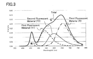
- FIG. 3 is a diagram showing an example of emission spectra obtained from the simulation.
- the spectrum shown in FIG 3 is an example obtained from the calculation result, which is a spectrum in line with a incandescent lamp color in the case of 541 nm for the emission peak wavelength ⁇ 1 of the fluorescent material on the shorter wavelength side and 599 nm for the emission peak wavelength ⁇ 2 of the fluorescent material on the longer wavelength side.
- the lumen equivalent is 264 Im/W, and Ra is 91.
- FIGS. 4A and 4B are diagrams showing simulation results in the present embodiment.
- FIG 4A shows the simulation results
- FIG. 4B is a diagram for explaining the function and effect.
- FIG. 4A and 4B for comparison, the characteristic curve in the case of the one kind of SION as shown in FIG. 2 is also shown by a solid line.
- respective points (marks) plotted refer to characteristic curves in the case of applying the two kinds of SION based fluorescent materials Y1 and Y2.
- the same mark represents a case in which the fluorescent material Y1 has the same peak wavelength ⁇ 1.
- FIG. 4A and 4B it has been found that there is a range in which the combination of the two kinds of fluorescent materials improves characteristics more than the one kind of fluorescent material.
- the range hatched with diagonal lines is a range which includes practical characteristics, and improves the characteristics more than in the case of one kind of fluorescent material. More specifically, the practically required Ra is generally 70 or more (a right range from a dotted line A), where there is a range in which a high luminescent efficiency is achieved at the same Ra as in the case of one kind of SION based fluorescent material (an upper range from the solid line), or a range in which Ra is achieved which is not able to be achieved by the SION-based fluorescent material (a right range from a dotted line B).
- FIG. 5 is a diagram for explaining the function and effect of the embodiment.
- the white light emitting device desirably satisfies the condition of 30 ⁇ ⁇ 2 - ⁇ 1.
- the satisfaction of this condition achieves characteristics in the upper right range from a dotted line C as shown in FIG. 5 . More specifically, in the upper right range from the inflection point of the characteristic curve according to the embodiment, the characteristics are improved more than in the case of the one kind of SION based fluorescent material.
- the condition is more desirably 40 ⁇ ⁇ 2 - ⁇ 1 for improving the luminescent efficiency.
- the white light emitting device desirably satisfies the condition of 1110 ⁇ ⁇ 1 + ⁇ 2.
- the satisfaction of this condition achieves characteristics in the upper range from a dotted line D as shown in FIG. 5 . More specifically, in the range in which the luminescent efficiency is always higher than in the case of reaching the highest Ra with the one kind of SION based fluorescent material, the characteristics are improved more than in the case of the one kind of SION based fluorescent material only.
- the white light emitting device desirably satisfies the condition of 530 ⁇ ⁇ 1 ⁇ 540.
- the satisfaction of this condition achieves characteristics in the always right range from a dotted line B as shown in FIG. 5 . More specifically, in the range always with Ra of 90 or more, the characteristics are improved more than in the case of the one kind of SION based fluorescent material.
- the fluorescent materials included in the fluorescent layer are desirably only the three kinds of fluorescent materials in total: the two kinds of yellow-green to orange fluorescent materials and the one kind of red fluorescent material.
- a white light emitting device which can achieve high color rendering properties and a high luminescent efficiency.
- a white light emitting device which has color deviations suppressed in high-temperature operation.
- a YAG : Ce fluorescent material As for the full width at half maximum, a typical value for the YAG : Ce fluorescent material were used. More specifically, a value of 110 nm was used for both Y1 on the shorter wavelength side and Y2 on the longer wavelength side.
- the Y1 on the shorter wavelength side desirably has 100 nm or less.
- the Y2 on the longer wavelength side desirably has 100 nm or less, and more desirably 80 nm or less.
- a white light emitting device is the same as in the first embodiment. Therefore, the contents overlapping with the first embodiment will not be repeated.
- FIG. 6 is a schematic cross-sectional view of the light emitting device according to the present embodiment.
- This light emitting device 20 is a white light emitting device which emits white light.
- the light emitting device 20 includes a fluorescent layer 26, in place of the first fluorescent layer 20 and second fluorescent layer 22 according to the first embodiment.
- the fluorescent layer 26 contains therein a mixture of a first fluorescent material which emits light with a first peak wavelength of 525 nm or more and 560 nm or less, with the use of light emitted from the light emitting element 14 as excitation light, and a second fluorescent material which emits light with a second peak wavelength longer than the first peak wavelength, with the use of light emitted from the light emitting element 14 as excitation light.
- a white light emitting device which can achieve high color rendering properties and a high luminescent efficiency.
- a white light emitting device is provided which has color deviations suppressed in high-temperature operation. Furthermore, the formation of the fluorescent layer is simple, thus facilitating the manufacture of the white light emitting device.
- the case of using the AlGalnN based LED with GaInN as the light emitting layer has been described as examples in the embodiments.
- LEDs can be also used which use an aluminum gallium indium nitride (AlGalnN) which is a Ill-V group compound semiconductor, or a magnesium zinc oxide (MgZnO) which is a II-VI group compound semiconductor, or the like as the light emitting layer (active layer).
- AlGalnN aluminum gallium indium nitride
- MgZnO magnesium zinc oxide
- the III-V group compound semiconductor to be used as the light emitting layer is a nitride semiconductor containing at least one selected from the group including Al, Ga, and In.
- This nitride semiconductor is specifically represented by Al x Ga y ln (1-x-y) N (0 ⁇ x ⁇ 1, 0 ⁇ y ⁇ 1, 0 ⁇ (x + y) ⁇ 1).
- This type of nitride semiconductor includes all of: binary compounds of AlN, GaN, and InN; ternary compounds of Al x Ga (1 -x) N (0 ⁇ x ⁇ 1), Al x ln (1-x) N (0 ⁇ x ⁇ 1), and Ga y ln (1-y) N (0 ⁇ y ⁇ 1); and further quaternary compounds containing all of the elements.
- the emission peak wavelength is determined in the range of ultraviolet to blue, on the basis of the composition of Al, Ga, and In: x, y, and (1 - x - y).
- some of the group III element can be substituted for boron (B), thallium (TI), and the like.
- some of N that is the group V element can be substituted for phosphorous (P), arsenic (As), antimony (Sb), bismuth (Bi) and the like.
- an oxide semiconductor containing at least one of Mg and Zn can be used as the II-VI group compound semiconductor to be used as the light emitting layer.
- the oxide semiconductor include semiconductors represented by Mg z Zn (1-z) O (0 ⁇ z ⁇ 1), and the emission peak wavelength in an ultraviolet range is determined on the basis of the composition of Mg and Zn: z and (1 - z).
- silicone resin as the transparent base material for the fluorescent layer has been described as an example, any material can be used which highly transmits the excitation light and has high heat resistance.
- a material for example, an epoxy resin, a urea resin, a fluorine resin, an acrylic resin, and a polyimide resin, etc. can be used in addition to silicone resin.
- the epoxy resin or the silicone resin is preferably used because of easy availability, easy handling, and moreover inexpensiveness.
- glass, a sintered body, etc. can be also used besides the resins.
- nitride fluorescent material and oxysulfide fluorescent material as well as oxynitrides, and the like can be used as the red fluorescent material.
- Nitride Based fluorescent material mainly a silicon nitride based fluorescent material
- Oxynitride Based fluorescent material L x si y N (2x/3 + 4y/3) :Eu or L x Si y O z N (2x/3 + 4y/3 - 2z/3) :Eu
- L represents at least one element selected from the group including Sr, Ca, and Sr and Ca
- Oxysulfide Fluorescent Material (Ln (1 - x) Eu x )O 2 S (Ln is at least one element selected from the group including Sc, Y, La, Gd, and Lu, and x is a numerical value which satisfies 0 ⁇ x ⁇ 1) Further, at least one selected from the group including Tb, Pr, Mg, Ti, Nb, Ta, Ga, Sm, and Tm may be contained as an activator agent.
Landscapes
- Chemical & Material Sciences (AREA)
- Inorganic Chemistry (AREA)
- Engineering & Computer Science (AREA)
- Materials Engineering (AREA)
- Organic Chemistry (AREA)
- Led Device Packages (AREA)
- Luminescent Compositions (AREA)
- Electroluminescent Light Sources (AREA)
Applications Claiming Priority (1)
| Application Number | Priority Date | Filing Date | Title |
|---|---|---|---|
| JP2012053378A JP5749201B2 (ja) | 2012-03-09 | 2012-03-09 | 白色発光装置 |
Publications (3)
| Publication Number | Publication Date |
|---|---|
| EP2636718A2 true EP2636718A2 (fr) | 2013-09-11 |
| EP2636718A3 EP2636718A3 (fr) | 2014-05-28 |
| EP2636718B1 EP2636718B1 (fr) | 2015-01-07 |
Family
ID=47748497
Family Applications (1)
| Application Number | Title | Priority Date | Filing Date |
|---|---|---|---|
| EP13156044.3A Active EP2636718B1 (fr) | 2012-03-09 | 2013-02-20 | Dispositif électroluminescent blanc |
Country Status (6)
| Country | Link |
|---|---|
| US (1) | US8836211B2 (fr) |
| EP (1) | EP2636718B1 (fr) |
| JP (1) | JP5749201B2 (fr) |
| KR (1) | KR20130103360A (fr) |
| CN (1) | CN103311413B (fr) |
| TW (1) | TWI489659B (fr) |
Families Citing this family (14)
| Publication number | Priority date | Publication date | Assignee | Title |
|---|---|---|---|---|
| US20140022761A1 (en) * | 2011-01-21 | 2014-01-23 | Osram Sylvania Inc. | Luminescent Converter and LED Light Source Containing Same |
| JP6081235B2 (ja) | 2013-03-07 | 2017-02-15 | 株式会社東芝 | 白色発光装置 |
| WO2015050317A1 (fr) * | 2013-10-02 | 2015-04-09 | 지엘비텍 주식회사 | Dispositif émetteur de lumière blanche à rendu de couleur élevé |
| KR101417874B1 (ko) * | 2013-10-02 | 2014-07-09 | 지엘비텍 주식회사 | 고연색성 백색 발광 소자 |
| CN107431112B (zh) * | 2015-04-03 | 2020-01-10 | 夏普株式会社 | 发光装置 |
| JP2017017059A (ja) * | 2015-06-26 | 2017-01-19 | パナソニックIpマネジメント株式会社 | 照明用光源及び照明装置 |
| KR102423748B1 (ko) * | 2015-07-08 | 2022-07-22 | 쑤저우 레킨 세미컨덕터 컴퍼니 리미티드 | 발광장치 |
| JP2017090625A (ja) * | 2015-11-09 | 2017-05-25 | 日本碍子株式会社 | 光学部品及びその製造方法 |
| US10236425B2 (en) * | 2016-03-08 | 2019-03-19 | Glbtech Co., Ltd. | White light emitting device having high color rendering |
| JP6526317B2 (ja) * | 2016-03-24 | 2019-06-05 | シャープ株式会社 | 光源装置および発光装置 |
| JP6906914B2 (ja) * | 2016-08-31 | 2021-07-21 | エルジー ディスプレイ カンパニー リミテッド | 波長選択素子、光源装置及び表示装置 |
| EP3648183B1 (fr) * | 2017-06-28 | 2022-08-24 | KYOCERA Corporation | Dispositif électroluminescent et dispositif d'éclairage |
| JP6769449B2 (ja) * | 2018-01-30 | 2020-10-14 | 日亜化学工業株式会社 | 照明装置 |
| CN115763672B (zh) * | 2023-01-09 | 2023-06-13 | 四川世纪和光科技发展有限公司 | 一种近自然光led封装构件、封装方法及照明装置 |
Family Cites Families (13)
| Publication number | Priority date | Publication date | Assignee | Title |
|---|---|---|---|---|
| JP4104013B2 (ja) * | 2005-03-18 | 2008-06-18 | 株式会社フジクラ | 発光デバイス及び照明装置 |
| JP4110417B2 (ja) | 2005-03-18 | 2008-07-02 | セイコーエプソン株式会社 | 面発光型装置及びその製造方法 |
| CN101501874B (zh) * | 2006-08-14 | 2012-04-04 | 株式会社藤仓 | 发光器件及照明装置 |
| JP5194675B2 (ja) * | 2006-10-31 | 2013-05-08 | 東芝ライテック株式会社 | 発光装置 |
| JP2008235552A (ja) * | 2007-03-20 | 2008-10-02 | Toshiba Lighting & Technology Corp | 発光装置の製造方法および発光装置 |
| CN101157854B (zh) * | 2007-07-02 | 2010-10-13 | 北京宇极科技发展有限公司 | 一种氮氧化合物发光材料、其制备方法及其应用 |
| WO2009017206A1 (fr) * | 2007-08-01 | 2009-02-05 | Mitsubishi Chemical Corporation | Matière luminescente et son procédé de fabrication, nitrure de silicium cristallin et son procédé de fabrication, composition contenant une substance luminescente, dispositif émettant de la lumière utilisant la substance luminescente, dispositif d'affichage d'image et dispositif d'é |
| JP5044329B2 (ja) | 2007-08-31 | 2012-10-10 | 株式会社東芝 | 発光装置 |
| WO2010041195A1 (fr) | 2008-10-09 | 2010-04-15 | Philips Intellectual Property & Standards Gmbh | Phosphore émettant de la lumière bleue |
| KR101163902B1 (ko) | 2010-08-10 | 2012-07-09 | 엘지이노텍 주식회사 | 발광 소자 |
| KR101077990B1 (ko) * | 2010-02-12 | 2011-10-31 | 삼성엘이디 주식회사 | 형광체, 발광장치, 면광원장치, 디스플레이 장치 및 조명장치 |
| JP5129283B2 (ja) * | 2010-03-09 | 2013-01-30 | 株式会社東芝 | 蛍光体、蛍光体の製造方法、発光装置及び発光モジュール |
| KR101625911B1 (ko) | 2010-03-10 | 2016-06-01 | 삼성전자주식회사 | 광효율이 개선된 led 장치 |
-
2012
- 2012-03-09 JP JP2012053378A patent/JP5749201B2/ja active Active
- 2012-08-29 US US13/597,808 patent/US8836211B2/en active Active
-
2013
- 2013-02-20 EP EP13156044.3A patent/EP2636718B1/fr active Active
- 2013-02-25 TW TW102106602A patent/TWI489659B/zh active
- 2013-02-26 KR KR1020130020225A patent/KR20130103360A/ko not_active Ceased
- 2013-02-28 CN CN201310063120.1A patent/CN103311413B/zh active Active
Also Published As
| Publication number | Publication date |
|---|---|
| KR20130103360A (ko) | 2013-09-23 |
| TWI489659B (zh) | 2015-06-21 |
| US20130234584A1 (en) | 2013-09-12 |
| EP2636718B1 (fr) | 2015-01-07 |
| JP5749201B2 (ja) | 2015-07-15 |
| CN103311413A (zh) | 2013-09-18 |
| EP2636718A3 (fr) | 2014-05-28 |
| JP2013187485A (ja) | 2013-09-19 |
| US8836211B2 (en) | 2014-09-16 |
| CN103311413B (zh) | 2015-11-18 |
| TW201401570A (zh) | 2014-01-01 |
Similar Documents
| Publication | Publication Date | Title |
|---|---|---|
| EP2636718B1 (fr) | Dispositif électroluminescent blanc | |
| JP7727121B2 (ja) | 異なる色度のledを有する照明デバイス | |
| KR101641377B1 (ko) | 백색광 방출 다이오드들(leds)을 위한 멀티플-칩 여기 시스템들 | |
| US9660152B2 (en) | System and method for selected pump LEDs with multiple phosphors | |
| JP4559496B2 (ja) | 発光装置 | |
| CN102686700B (zh) | 卤磷酸盐荧光体及白色发光装置 | |
| US7753553B2 (en) | Illumination system comprising color deficiency compensating luminescent material | |
| TW201720908A (zh) | 用於一般照明與顯示器背光源之磷光體轉換白光發光裝置及光致發光化合物 | |
| US20130234591A1 (en) | White light emitting device | |
| US9190582B2 (en) | Light emitting device | |
| JP2003110150A (ja) | 半導体発光素子とこれを用いた発光装置 | |
| JP4151284B2 (ja) | 窒化物半導体発光素子及び発光装置並びにそれらの製造方法 | |
| US10150912B2 (en) | Red phosphor, white light emitting apparatus, display apparatus, and lighting apparatus | |
| JP4411841B2 (ja) | 発光装置及びそれを用いた照明装置並びにディスプレイ | |
| KR101176212B1 (ko) | 알카리 토류 포스포러스 나이트라이드계 형광체와 그 제조방법 및 이를 이용한 발광장치 | |
| JP2006104413A (ja) | 蛍光体およびそれを用いた白色発光素子 | |
| JP4604516B2 (ja) | 発光装置及びそれを用いた照明装置並びにディスプレイ | |
| JP2015183084A (ja) | 紫光励起用蛍光体、該蛍光体を用いた蛍光体含有組成物及び発光装置、並びに、該発光装置を用いた照明装置及び画像表示装置 | |
| US20230420619A1 (en) | System and method for selected pump leds with multiple phosphors | |
| US11901492B2 (en) | High color rendering white light emitting devices and high color rendering photoluminescence compositions |
Legal Events
| Date | Code | Title | Description |
|---|---|---|---|
| PUAI | Public reference made under article 153(3) epc to a published international application that has entered the european phase |
Free format text: ORIGINAL CODE: 0009012 |
|
| 17P | Request for examination filed |
Effective date: 20130220 |
|
| AK | Designated contracting states |
Kind code of ref document: A2 Designated state(s): AL AT BE BG CH CY CZ DE DK EE ES FI FR GB GR HR HU IE IS IT LI LT LU LV MC MK MT NL NO PL PT RO RS SE SI SK SM TR |
|
| AX | Request for extension of the european patent |
Extension state: BA ME |
|
| PUAL | Search report despatched |
Free format text: ORIGINAL CODE: 0009013 |
|
| AK | Designated contracting states |
Kind code of ref document: A3 Designated state(s): AL AT BE BG CH CY CZ DE DK EE ES FI FR GB GR HR HU IE IS IT LI LT LU LV MC MK MT NL NO PL PT RO RS SE SI SK SM TR |
|
| AX | Request for extension of the european patent |
Extension state: BA ME |
|
| RIC1 | Information provided on ipc code assigned before grant |
Ipc: C09K 11/59 20060101AFI20140424BHEP Ipc: H01L 33/50 20100101ALI20140424BHEP |
|
| REG | Reference to a national code |
Ref country code: DE Ref legal event code: R079 Ref document number: 602013000772 Country of ref document: DE Free format text: PREVIOUS MAIN CLASS: C09K0011770000 Ipc: C09K0011590000 |
|
| GRAP | Despatch of communication of intention to grant a patent |
Free format text: ORIGINAL CODE: EPIDOSNIGR1 |
|
| INTG | Intention to grant announced |
Effective date: 20140723 |
|
| RIC1 | Information provided on ipc code assigned before grant |
Ipc: H01L 33/50 20100101ALI20140711BHEP Ipc: C09K 11/59 20060101AFI20140711BHEP |
|
| GRAS | Grant fee paid |
Free format text: ORIGINAL CODE: EPIDOSNIGR3 |
|
| GRAA | (expected) grant |
Free format text: ORIGINAL CODE: 0009210 |
|
| AK | Designated contracting states |
Kind code of ref document: B1 Designated state(s): AL AT BE BG CH CY CZ DE DK EE ES FI FR GB GR HR HU IE IS IT LI LT LU LV MC MK MT NL NO PL PT RO RS SE SI SK SM TR |
|
| REG | Reference to a national code |
Ref country code: GB Ref legal event code: FG4D |
|
| REG | Reference to a national code |
Ref country code: CH Ref legal event code: EP |
|
| REG | Reference to a national code |
Ref country code: IE Ref legal event code: FG4D |
|
| REG | Reference to a national code |
Ref country code: AT Ref legal event code: REF Ref document number: 705724 Country of ref document: AT Kind code of ref document: T Effective date: 20150215 |
|
| REG | Reference to a national code |
Ref country code: DE Ref legal event code: R096 Ref document number: 602013000772 Country of ref document: DE Effective date: 20150219 |
|
| REG | Reference to a national code |
Ref country code: NL Ref legal event code: VDEP Effective date: 20150107 |
|
| REG | Reference to a national code |
Ref country code: AT Ref legal event code: MK05 Ref document number: 705724 Country of ref document: AT Kind code of ref document: T Effective date: 20150107 |
|
| REG | Reference to a national code |
Ref country code: LT Ref legal event code: MG4D |
|
| PG25 | Lapsed in a contracting state [announced via postgrant information from national office to epo] |
Ref country code: BE Free format text: LAPSE BECAUSE OF NON-PAYMENT OF DUE FEES Effective date: 20150228 |
|
| PG25 | Lapsed in a contracting state [announced via postgrant information from national office to epo] |
Ref country code: SE Free format text: LAPSE BECAUSE OF FAILURE TO SUBMIT A TRANSLATION OF THE DESCRIPTION OR TO PAY THE FEE WITHIN THE PRESCRIBED TIME-LIMIT Effective date: 20150107 Ref country code: BG Free format text: LAPSE BECAUSE OF FAILURE TO SUBMIT A TRANSLATION OF THE DESCRIPTION OR TO PAY THE FEE WITHIN THE PRESCRIBED TIME-LIMIT Effective date: 20150407 Ref country code: NO Free format text: LAPSE BECAUSE OF FAILURE TO SUBMIT A TRANSLATION OF THE DESCRIPTION OR TO PAY THE FEE WITHIN THE PRESCRIBED TIME-LIMIT Effective date: 20150407 Ref country code: HR Free format text: LAPSE BECAUSE OF FAILURE TO SUBMIT A TRANSLATION OF THE DESCRIPTION OR TO PAY THE FEE WITHIN THE PRESCRIBED TIME-LIMIT Effective date: 20150107 Ref country code: ES Free format text: LAPSE BECAUSE OF FAILURE TO SUBMIT A TRANSLATION OF THE DESCRIPTION OR TO PAY THE FEE WITHIN THE PRESCRIBED TIME-LIMIT Effective date: 20150107 Ref country code: FI Free format text: LAPSE BECAUSE OF FAILURE TO SUBMIT A TRANSLATION OF THE DESCRIPTION OR TO PAY THE FEE WITHIN THE PRESCRIBED TIME-LIMIT Effective date: 20150107 Ref country code: LT Free format text: LAPSE BECAUSE OF FAILURE TO SUBMIT A TRANSLATION OF THE DESCRIPTION OR TO PAY THE FEE WITHIN THE PRESCRIBED TIME-LIMIT Effective date: 20150107 |
|
| PG25 | Lapsed in a contracting state [announced via postgrant information from national office to epo] |
Ref country code: GR Free format text: LAPSE BECAUSE OF FAILURE TO SUBMIT A TRANSLATION OF THE DESCRIPTION OR TO PAY THE FEE WITHIN THE PRESCRIBED TIME-LIMIT Effective date: 20150408 Ref country code: NL Free format text: LAPSE BECAUSE OF FAILURE TO SUBMIT A TRANSLATION OF THE DESCRIPTION OR TO PAY THE FEE WITHIN THE PRESCRIBED TIME-LIMIT Effective date: 20150107 Ref country code: RS Free format text: LAPSE BECAUSE OF FAILURE TO SUBMIT A TRANSLATION OF THE DESCRIPTION OR TO PAY THE FEE WITHIN THE PRESCRIBED TIME-LIMIT Effective date: 20150107 Ref country code: AT Free format text: LAPSE BECAUSE OF FAILURE TO SUBMIT A TRANSLATION OF THE DESCRIPTION OR TO PAY THE FEE WITHIN THE PRESCRIBED TIME-LIMIT Effective date: 20150107 Ref country code: PL Free format text: LAPSE BECAUSE OF FAILURE TO SUBMIT A TRANSLATION OF THE DESCRIPTION OR TO PAY THE FEE WITHIN THE PRESCRIBED TIME-LIMIT Effective date: 20150107 Ref country code: IS Free format text: LAPSE BECAUSE OF FAILURE TO SUBMIT A TRANSLATION OF THE DESCRIPTION OR TO PAY THE FEE WITHIN THE PRESCRIBED TIME-LIMIT Effective date: 20150507 Ref country code: LV Free format text: LAPSE BECAUSE OF FAILURE TO SUBMIT A TRANSLATION OF THE DESCRIPTION OR TO PAY THE FEE WITHIN THE PRESCRIBED TIME-LIMIT Effective date: 20150107 |
|
| REG | Reference to a national code |
Ref country code: DE Ref legal event code: R097 Ref document number: 602013000772 Country of ref document: DE |
|
| PG25 | Lapsed in a contracting state [announced via postgrant information from national office to epo] |
Ref country code: CZ Free format text: LAPSE BECAUSE OF FAILURE TO SUBMIT A TRANSLATION OF THE DESCRIPTION OR TO PAY THE FEE WITHIN THE PRESCRIBED TIME-LIMIT Effective date: 20150107 Ref country code: RO Free format text: LAPSE BECAUSE OF FAILURE TO SUBMIT A TRANSLATION OF THE DESCRIPTION OR TO PAY THE FEE WITHIN THE PRESCRIBED TIME-LIMIT Effective date: 20150107 Ref country code: EE Free format text: LAPSE BECAUSE OF FAILURE TO SUBMIT A TRANSLATION OF THE DESCRIPTION OR TO PAY THE FEE WITHIN THE PRESCRIBED TIME-LIMIT Effective date: 20150107 Ref country code: MC Free format text: LAPSE BECAUSE OF FAILURE TO SUBMIT A TRANSLATION OF THE DESCRIPTION OR TO PAY THE FEE WITHIN THE PRESCRIBED TIME-LIMIT Effective date: 20150107 Ref country code: DK Free format text: LAPSE BECAUSE OF FAILURE TO SUBMIT A TRANSLATION OF THE DESCRIPTION OR TO PAY THE FEE WITHIN THE PRESCRIBED TIME-LIMIT Effective date: 20150107 Ref country code: SK Free format text: LAPSE BECAUSE OF FAILURE TO SUBMIT A TRANSLATION OF THE DESCRIPTION OR TO PAY THE FEE WITHIN THE PRESCRIBED TIME-LIMIT Effective date: 20150107 |
|
| PLBE | No opposition filed within time limit |
Free format text: ORIGINAL CODE: 0009261 |
|
| STAA | Information on the status of an ep patent application or granted ep patent |
Free format text: STATUS: NO OPPOSITION FILED WITHIN TIME LIMIT |
|
| REG | Reference to a national code |
Ref country code: IE Ref legal event code: MM4A |
|
| 26N | No opposition filed |
Effective date: 20151008 |
|
| PG25 | Lapsed in a contracting state [announced via postgrant information from national office to epo] |
Ref country code: IT Free format text: LAPSE BECAUSE OF FAILURE TO SUBMIT A TRANSLATION OF THE DESCRIPTION OR TO PAY THE FEE WITHIN THE PRESCRIBED TIME-LIMIT Effective date: 20150107 |
|
| REG | Reference to a national code |
Ref country code: FR Ref legal event code: PLFP Year of fee payment: 4 |
|
| PG25 | Lapsed in a contracting state [announced via postgrant information from national office to epo] |
Ref country code: IE Free format text: LAPSE BECAUSE OF NON-PAYMENT OF DUE FEES Effective date: 20150220 |
|
| PG25 | Lapsed in a contracting state [announced via postgrant information from national office to epo] |
Ref country code: SI Free format text: LAPSE BECAUSE OF FAILURE TO SUBMIT A TRANSLATION OF THE DESCRIPTION OR TO PAY THE FEE WITHIN THE PRESCRIBED TIME-LIMIT Effective date: 20150107 |
|
| PG25 | Lapsed in a contracting state [announced via postgrant information from national office to epo] |
Ref country code: BE Free format text: LAPSE BECAUSE OF FAILURE TO SUBMIT A TRANSLATION OF THE DESCRIPTION OR TO PAY THE FEE WITHIN THE PRESCRIBED TIME-LIMIT Effective date: 20150107 |
|
| REG | Reference to a national code |
Ref country code: CH Ref legal event code: PL |
|
| PG25 | Lapsed in a contracting state [announced via postgrant information from national office to epo] |
Ref country code: LI Free format text: LAPSE BECAUSE OF NON-PAYMENT OF DUE FEES Effective date: 20160229 Ref country code: CH Free format text: LAPSE BECAUSE OF NON-PAYMENT OF DUE FEES Effective date: 20160229 |
|
| PG25 | Lapsed in a contracting state [announced via postgrant information from national office to epo] |
Ref country code: MT Free format text: LAPSE BECAUSE OF FAILURE TO SUBMIT A TRANSLATION OF THE DESCRIPTION OR TO PAY THE FEE WITHIN THE PRESCRIBED TIME-LIMIT Effective date: 20150107 |
|
| REG | Reference to a national code |
Ref country code: FR Ref legal event code: PLFP Year of fee payment: 5 |
|
| PG25 | Lapsed in a contracting state [announced via postgrant information from national office to epo] |
Ref country code: HU Free format text: LAPSE BECAUSE OF FAILURE TO SUBMIT A TRANSLATION OF THE DESCRIPTION OR TO PAY THE FEE WITHIN THE PRESCRIBED TIME-LIMIT; INVALID AB INITIO Effective date: 20130220 |
|
| PG25 | Lapsed in a contracting state [announced via postgrant information from national office to epo] |
Ref country code: CY Free format text: LAPSE BECAUSE OF FAILURE TO SUBMIT A TRANSLATION OF THE DESCRIPTION OR TO PAY THE FEE WITHIN THE PRESCRIBED TIME-LIMIT Effective date: 20150107 |
|
| PG25 | Lapsed in a contracting state [announced via postgrant information from national office to epo] |
Ref country code: TR Free format text: LAPSE BECAUSE OF FAILURE TO SUBMIT A TRANSLATION OF THE DESCRIPTION OR TO PAY THE FEE WITHIN THE PRESCRIBED TIME-LIMIT Effective date: 20150107 |
|
| PG25 | Lapsed in a contracting state [announced via postgrant information from national office to epo] |
Ref country code: LU Free format text: LAPSE BECAUSE OF NON-PAYMENT OF DUE FEES Effective date: 20150220 |
|
| REG | Reference to a national code |
Ref country code: FR Ref legal event code: PLFP Year of fee payment: 6 |
|
| PG25 | Lapsed in a contracting state [announced via postgrant information from national office to epo] |
Ref country code: SM Free format text: LAPSE BECAUSE OF FAILURE TO SUBMIT A TRANSLATION OF THE DESCRIPTION OR TO PAY THE FEE WITHIN THE PRESCRIBED TIME-LIMIT Effective date: 20150107 |
|
| PG25 | Lapsed in a contracting state [announced via postgrant information from national office to epo] |
Ref country code: MK Free format text: LAPSE BECAUSE OF FAILURE TO SUBMIT A TRANSLATION OF THE DESCRIPTION OR TO PAY THE FEE WITHIN THE PRESCRIBED TIME-LIMIT Effective date: 20150107 Ref country code: PT Free format text: LAPSE BECAUSE OF FAILURE TO SUBMIT A TRANSLATION OF THE DESCRIPTION OR TO PAY THE FEE WITHIN THE PRESCRIBED TIME-LIMIT Effective date: 20150107 |
|
| REG | Reference to a national code |
Ref country code: DE Ref legal event code: R082 Ref document number: 602013000772 Country of ref document: DE Representative=s name: HOFFMANN - EITLE PATENT- UND RECHTSANWAELTE PA, DE Ref country code: DE Ref legal event code: R081 Ref document number: 602013000772 Country of ref document: DE Owner name: TOSHIBA ELECTRONIC DEVICES & STORAGE CORPORATI, JP Free format text: FORMER OWNER: KABUSHIKI KAISHA TOSHIBA, TOKYO, JP Ref country code: DE Ref legal event code: R081 Ref document number: 602013000772 Country of ref document: DE Owner name: SAMSUNG ELECTRONICS CO., LTD., SUWON-SI, KR Free format text: FORMER OWNER: KABUSHIKI KAISHA TOSHIBA, TOKYO, JP Ref country code: DE Ref legal event code: R082 Ref document number: 602013000772 Country of ref document: DE Representative=s name: KUHNEN & WACKER PATENT- UND RECHTSANWALTSBUERO, DE |
|
| REG | Reference to a national code |
Ref country code: GB Ref legal event code: 732E Free format text: REGISTERED BETWEEN 20180621 AND 20180627 |
|
| REG | Reference to a national code |
Ref country code: DE Ref legal event code: R082 Ref document number: 602013000772 Country of ref document: DE Representative=s name: KUHNEN & WACKER PATENT- UND RECHTSANWALTSBUERO, DE Ref country code: DE Ref legal event code: R081 Ref document number: 602013000772 Country of ref document: DE Owner name: SAMSUNG ELECTRONICS CO., LTD., SUWON-SI, KR Free format text: FORMER OWNER: TOSHIBA ELECTRONIC DEVICES & STORAGE CORPORATION, TOKYO, JP Ref country code: DE Ref legal event code: R081 Ref document number: 602013000772 Country of ref document: DE Owner name: SAMSUNG ELECTRONICS CO., LTD., SUWON-SI, KR Free format text: FORMER OWNER: TOSHIBA ELECTRONIC DEVICES & STORAGE CORP., TOKYO, JP |
|
| PG25 | Lapsed in a contracting state [announced via postgrant information from national office to epo] |
Ref country code: AL Free format text: LAPSE BECAUSE OF FAILURE TO SUBMIT A TRANSLATION OF THE DESCRIPTION OR TO PAY THE FEE WITHIN THE PRESCRIBED TIME-LIMIT Effective date: 20150107 |
|
| REG | Reference to a national code |
Ref country code: FR Ref legal event code: TP Owner name: TOSHIBA ELECTRONIC DEVICES & STORAGE CORPORATI, JP Effective date: 20181001 |
|
| REG | Reference to a national code |
Ref country code: GB Ref legal event code: 732E Free format text: REGISTERED BETWEEN 20190124 AND 20190130 |
|
| P01 | Opt-out of the competence of the unified patent court (upc) registered |
Effective date: 20230524 |
|
| PGFP | Annual fee paid to national office [announced via postgrant information from national office to epo] |
Ref country code: DE Payment date: 20241224 Year of fee payment: 13 |
|
| PGFP | Annual fee paid to national office [announced via postgrant information from national office to epo] |
Ref country code: GB Payment date: 20250102 Year of fee payment: 13 |
|
| PGFP | Annual fee paid to national office [announced via postgrant information from national office to epo] |
Ref country code: FR Payment date: 20251222 Year of fee payment: 14 |