EP2637206A2 - Dispositif d'éclairage - Google Patents
Dispositif d'éclairage Download PDFInfo
- Publication number
- EP2637206A2 EP2637206A2 EP13158105.0A EP13158105A EP2637206A2 EP 2637206 A2 EP2637206 A2 EP 2637206A2 EP 13158105 A EP13158105 A EP 13158105A EP 2637206 A2 EP2637206 A2 EP 2637206A2
- Authority
- EP
- European Patent Office
- Prior art keywords
- light
- lighting device
- light source
- source unit
- lens
- Prior art date
- Legal status (The legal status is an assumption and is not a legal conclusion. Google has not performed a legal analysis and makes no representation as to the accuracy of the status listed.)
- Granted
Links
Images


Classifications
-
- H—ELECTRICITY
- H10—SEMICONDUCTOR DEVICES; ELECTRIC SOLID-STATE DEVICES NOT OTHERWISE PROVIDED FOR
- H10H—INORGANIC LIGHT-EMITTING SEMICONDUCTOR DEVICES HAVING POTENTIAL BARRIERS
- H10H20/00—Individual inorganic light-emitting semiconductor devices having potential barriers, e.g. light-emitting diodes [LED]
- H10H20/80—Constructional details
- H10H20/85—Packages
-
- F—MECHANICAL ENGINEERING; LIGHTING; HEATING; WEAPONS; BLASTING
- F21—LIGHTING
- F21V—FUNCTIONAL FEATURES OR DETAILS OF LIGHTING DEVICES OR SYSTEMS THEREOF; STRUCTURAL COMBINATIONS OF LIGHTING DEVICES WITH OTHER ARTICLES, NOT OTHERWISE PROVIDED FOR
- F21V5/00—Refractors for light sources
- F21V5/008—Combination of two or more successive refractors along an optical axis
-
- F—MECHANICAL ENGINEERING; LIGHTING; HEATING; WEAPONS; BLASTING
- F21—LIGHTING
- F21V—FUNCTIONAL FEATURES OR DETAILS OF LIGHTING DEVICES OR SYSTEMS THEREOF; STRUCTURAL COMBINATIONS OF LIGHTING DEVICES WITH OTHER ARTICLES, NOT OTHERWISE PROVIDED FOR
- F21V21/00—Supporting, suspending, or attaching arrangements for lighting devices; Hand grips
- F21V21/14—Adjustable mountings
-
- F—MECHANICAL ENGINEERING; LIGHTING; HEATING; WEAPONS; BLASTING
- F21—LIGHTING
- F21V—FUNCTIONAL FEATURES OR DETAILS OF LIGHTING DEVICES OR SYSTEMS THEREOF; STRUCTURAL COMBINATIONS OF LIGHTING DEVICES WITH OTHER ARTICLES, NOT OTHERWISE PROVIDED FOR
- F21V5/00—Refractors for light sources
- F21V5/04—Refractors for light sources of lens shape
-
- G—PHYSICS
- G09—EDUCATION; CRYPTOGRAPHY; DISPLAY; ADVERTISING; SEALS
- G09F—DISPLAYING; ADVERTISING; SIGNS; LABELS OR NAME-PLATES; SEALS
- G09F13/00—Illuminated signs; Luminous advertising
- G09F13/04—Signs, boards or panels, illuminated from behind the insignia
-
- H—ELECTRICITY
- H05—ELECTRIC TECHNIQUES NOT OTHERWISE PROVIDED FOR
- H05K—PRINTED CIRCUITS; CASINGS OR CONSTRUCTIONAL DETAILS OF ELECTRIC APPARATUS; MANUFACTURE OF ASSEMBLAGES OF ELECTRICAL COMPONENTS
- H05K1/00—Printed circuits
- H05K1/02—Details
- H05K1/0274—Optical details, e.g. printed circuits comprising integral optical means
-
- F—MECHANICAL ENGINEERING; LIGHTING; HEATING; WEAPONS; BLASTING
- F21—LIGHTING
- F21V—FUNCTIONAL FEATURES OR DETAILS OF LIGHTING DEVICES OR SYSTEMS THEREOF; STRUCTURAL COMBINATIONS OF LIGHTING DEVICES WITH OTHER ARTICLES, NOT OTHERWISE PROVIDED FOR
- F21V13/00—Producing particular characteristics or distribution of the light emitted by means of a combination of elements specified in two or more of main groups F21V1/00 - F21V11/00
- F21V13/02—Combinations of only two kinds of elements
- F21V13/04—Combinations of only two kinds of elements the elements being reflectors and refractors
-
- F—MECHANICAL ENGINEERING; LIGHTING; HEATING; WEAPONS; BLASTING
- F21—LIGHTING
- F21Y—INDEXING SCHEME ASSOCIATED WITH SUBCLASSES F21K, F21L, F21S and F21V, RELATING TO THE FORM OR THE KIND OF THE LIGHT SOURCES OR OF THE COLOUR OF THE LIGHT EMITTED
- F21Y2105/00—Planar light sources
- F21Y2105/10—Planar light sources comprising a two-dimensional [2D] array of point-like light-generating elements
-
- F—MECHANICAL ENGINEERING; LIGHTING; HEATING; WEAPONS; BLASTING
- F21—LIGHTING
- F21Y—INDEXING SCHEME ASSOCIATED WITH SUBCLASSES F21K, F21L, F21S and F21V, RELATING TO THE FORM OR THE KIND OF THE LIGHT SOURCES OR OF THE COLOUR OF THE LIGHT EMITTED
- F21Y2115/00—Light-generating elements of semiconductor light sources
- F21Y2115/10—Light-emitting diodes [LED]
-
- H—ELECTRICITY
- H05—ELECTRIC TECHNIQUES NOT OTHERWISE PROVIDED FOR
- H05K—PRINTED CIRCUITS; CASINGS OR CONSTRUCTIONAL DETAILS OF ELECTRIC APPARATUS; MANUFACTURE OF ASSEMBLAGES OF ELECTRICAL COMPONENTS
- H05K1/00—Printed circuits
- H05K1/18—Printed circuits structurally associated with non-printed electric components
- H05K1/189—Printed circuits structurally associated with non-printed electric components characterised by the use of flexible or folded printed circuits
-
- H—ELECTRICITY
- H05—ELECTRIC TECHNIQUES NOT OTHERWISE PROVIDED FOR
- H05K—PRINTED CIRCUITS; CASINGS OR CONSTRUCTIONAL DETAILS OF ELECTRIC APPARATUS; MANUFACTURE OF ASSEMBLAGES OF ELECTRICAL COMPONENTS
- H05K2201/00—Indexing scheme relating to printed circuits covered by H05K1/00
- H05K2201/10—Details of components or other objects attached to or integrated in a printed circuit board
- H05K2201/10007—Types of components
- H05K2201/10106—Light emitting diode [LED]
-
- H—ELECTRICITY
- H05—ELECTRIC TECHNIQUES NOT OTHERWISE PROVIDED FOR
- H05K—PRINTED CIRCUITS; CASINGS OR CONSTRUCTIONAL DETAILS OF ELECTRIC APPARATUS; MANUFACTURE OF ASSEMBLAGES OF ELECTRICAL COMPONENTS
- H05K2201/00—Indexing scheme relating to printed circuits covered by H05K1/00
- H05K2201/20—Details of printed circuits not provided for in H05K2201/01 - H05K2201/10
- H05K2201/2054—Light-reflecting surface, e.g. conductors, substrates, coatings, dielectrics
-
- H—ELECTRICITY
- H05—ELECTRIC TECHNIQUES NOT OTHERWISE PROVIDED FOR
- H05K—PRINTED CIRCUITS; CASINGS OR CONSTRUCTIONAL DETAILS OF ELECTRIC APPARATUS; MANUFACTURE OF ASSEMBLAGES OF ELECTRICAL COMPONENTS
- H05K3/00—Apparatus or processes for manufacturing printed circuits
- H05K3/22—Secondary treatment of printed circuits
- H05K3/28—Applying non-metallic protective coatings
- H05K3/284—Applying non-metallic protective coatings for encapsulating mounted components
-
- H—ELECTRICITY
- H10—SEMICONDUCTOR DEVICES; ELECTRIC SOLID-STATE DEVICES NOT OTHERWISE PROVIDED FOR
- H10H—INORGANIC LIGHT-EMITTING SEMICONDUCTOR DEVICES HAVING POTENTIAL BARRIERS
- H10H20/00—Individual inorganic light-emitting semiconductor devices having potential barriers, e.g. light-emitting diodes [LED]
- H10H20/80—Constructional details
- H10H20/85—Packages
- H10H20/855—Optical field-shaping means, e.g. lenses
Definitions
- the present invention relates to the technical field of a lighting device, and more specifically, to a lighting device, which reduces an entire volume and weight by integrally forming a light source unit formed using a resin layer and a lens unit.
- An LED (Light Emitted Diode) device is a device which converts an electrical signal to infrared rays or light using a composition semiconductor property. Unlike a florescent lamp, since the LED device does not use harmful substances such as mercury and the like, it has a low possibility to cause environmental pollution and a long life span compared to a conventional light source. Also, it is advantageous that the LED device spends low electricity compared to the conventional light source and has excellent visibility and low brilliantness due to a high color temperature.
- a current lighting device has been developed from a structure, in which a traditional light source such as a conventional incandescent lamp or a florescent lamp is used, to a structure, in which the aforesaid LED device is used as a light source.
- a lighting device using an LED device and a lens as disclosed in Korean Laid-Open Patent Publication No. 10-2010-0132273 has been suggested.
- FIG. 1 schematically illustrates a structure of a conventional lighting device.
- the conventional lighting device includes: a light source unit 10 having a LED device; a front lens 50 which collects light irradiated from the light source unit 10 in a forward direction; an external housing 70. Furthermore, a cap 30 for protecting the front lens 50 and the light source unit 10 may be further formed. At this time, the cap 30 may perform the function of a separate lens.
- the conventional lighting device is generally configured such that a reflection member is disposed in an inner side of the external housing 70 to reflect light irradiated from the LED which is a point light source.
- a fixed space 40 is necessarily provided in an inner part of the external housing 70.
- the conventional lighting device requires the fixed space to improve a light reflection capability.
- An aspect of the present invention provides a structure of a lighting device which enables an entire thickness to get thin by integrally forming a lens unit and a light source unit.
- Another aspect of the present invention provides a structure of a lighting device which is configured such that a light source unit itself has flexibility so that a degree of freedom in product design can be improved and reliability can be secured.
- a lighting device including: a lens unit including one or more lenses; and a light source unit which converts light emitted from a light emitting unit to a surface light source and supplies the light to the lens unit, wherein the light source unit and the lens unit are formed in a structure in which they are integrally connected to each other.
- an entire thickness and volume of the lighting device can be reduced by integrally forming the lens unit and the light source unit, and a degree of freedom in design of the lighting device can be improved.
- the lens unit and the light source unit can be integrated regardless of a shape of the lens unit because the light source unit itself is formed to have constant flexibility.
- optical loss generated between the lens unit and the light source unit is minimized, light efficiency of the lighting device can be improved.
- the reflection member and the reflection pattern which can efficiently reflect the light emitted from the light emitting unit, are disposed in the light source unit, the reflectance of light and brightness can be maximized, and a uniform surface light source can be provided.
- FIG. 1 schematically illustrates a structure of a conventional lighting device.
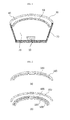
- FIG. 2 illustrates a rough structure of a lighting device according to the present invention.
- FIG. 3 illustrates a main structure of a light source unit of the lighting device illustrated in FIG. 2 .
- FIG. 4 illustrates a structure in which beads and a reflection member are added to the light source unit illustrated in FIG. 3 .
- FIG. 5 illustrates a structure in which the reflection member and an optical sheet are added to the light source unit illustrated in FIG. 3 .
- FIG. 6 illustrates a structure in which an adhesive layer is formed in the lighting device of the present invention illustrated in FIG. 5 .
- the gist of the present invention is to provide a structure of a lighting device, which can innovatively reduce an entire thickness by integrally forming a lens unit and a light source unit, and can also secure flexibility and improve a degree of freedom in design.
- the lighting device according to the present invention can be applied to various lamp devices such as a lamp for vehicles, a lighting device for home use, and an industrial lighting device, which require illumination.
- the lighting device can be also applied to headlights, car indoor illumination, door scuff, backlight and the like.
- the lighting device according to the present invention can be applied to the field of a backlight unit applied to a liquid crystal display device.
- the lighting device can be applied to all fields relating to illumination, which have been developed and commercialized or can be implemented according to future technical development.
- FIG. 2 illustrates a rough structure of a lighting device according to the present invention. More specifically, (a) of FIG. 2 illustrates the lighting device corresponding to a case in which a lens unit is composed of one lens (the outer lens), and (b) of FIG. 2 illustrates the lighting device corresponding to a case in which the lens unit is composed of two or more lens (including the outer lens and the inner lens).
- the lighting device of the present exemplary embodiment includes an outer lens 300 and a light source unit 100 connected to the outer lens 300.
- the light source unit 100 includes a light emitting unit in an inner part thereof, converts light emitted from the light emitting unit to a surface light source and emits the light to the outer lens 300. Furthermore, the light source unit 100 is formed on an inner side of the outer lens 300. At this time, a combination of the light source unit 100 and the outer lens 300 may be realized by an adhesive material. In addition to this, the combination may be also performed in such a way that the light source unit 100 is directly adhered to the outer lens 300. Meanwhile, in particular, the light source unit 100 of the present invention is formed in a structure in which the light guide plate is removed and the resin layer is formed. More specific explanation will be described in the explanation of FIG. 3 to FIG. 6 .
- the outer lens 300 concentrates light emitted from the light source unit 100 and converts the light to parallel light.
- the outer lens 300 may simultaneously perform the function of a cap for protecting inner configurations of the lighting device. All materials having light transmission may be used as a material of the outer lens 300 without a limitation.
- the outer lens 300 may be formed of a glass material, a PC (polycarbonate) material, a PMMA (polymethylmethacrlate) material, other polymer resins and the like.
- the lens unit is composed of the outer lens 300 and an inner lens 500.
- the light source unit 100 is formed in a structure in which it is connected to the inner lens 500, and more specifically, a structure in which it is connected to an inner side of the inner lens 500.
- the combination of the light source unit 100 and the inner lens 500 may be realized by an adhesive material.
- the combination may be also realized in such a way that the light source unit is directly adhered to the inner lens 500.
- the explanation regarding a material for forming the inner lens 500 except for the above explanation is identical with as that of the outer lens 300. Thus, the explanation thereon is omitted.
- the light emitted to the outside may be converted to diffusion light, parallel light and the like.
- the inner lens 500 primarily concentrates the light and converts it to parallel light.
- the outer lens 300 secondarily concentrates the light emitted from the inner lens 500 and converts it to more accurate parallel light, thereby emitting the light to the outside.
- a lens air gap 400 may be further formed between the inner lens 500 and the outer lens 300 so that the light passing through the inner lens 500 is uniformly diffused and is thus supplied to the outer lens 300. That is, thanks to the formation of the lens air gap 400, uniformity of the light supplied to the outer lens 300 can be improved. As a result, the uniformity of the light diffused and emitted through the outer lens 300 can be improved.
- the lens unit and the light source unit are integrated, an entire thickness and volume of the lighting device can be reduced. Furthermore, as the thickness and volume are reduced, a degree of freedom in design of the lighting device can be improved and the lighting device can be applied to various fields relating to illumination. Moreover, as the lens unit and the light source unit are formed to be closely adhered to each other, light loss generated between the lens unit and the light source unit may be minimized, thereby improving light efficiency of the lighting device.
- FIG. 3 illustrates a main structure of a light source unit of the lighting device illustrated in FIG. 2 .
- a light source unit 100a of the present invention may be include: a printed circuit board 110; one or more light emitting units 130 formed on the printed circuit board 110; the resin layer 150 which is formed on the light emitting unit 130 so that the light emitting unit 130 is embedded therein, and guides emitted light forward. Furthermore, it may further include a diffusion plate 290 which uniformly diffuses light incident from the resin layer and emits the light to the outside. Also, a prism sheet and a protective sheet may be further provided into an upper part or a lower part of the diffusion plate 290, even though this is not illustrated.
- the printed circuit board 110 means a board in which a circuit pattern is formed on the board, namely, a PCB.
- the printed circuit board according to the present invention may be formed as a flexible printed circuit board (FPCB).
- the light emitting units 130 are configured such that one or more light emitting units are arranged on the printed circuit board 110 so that light is emitted.
- the light emitting units 130 of the present invention may be composed of side view type light emitting diodes. That is, light emitting diodes having a structure in which the emitted light is emitted in a lateral direction rather than going straight up may be used as the light emitting units 130 of the present invention.
- the light source unit 100a is configured such that the light emitting units 130 composed of the side view type light emitting diodes are disposed in a direct type.
- the resin layer which functions to diffuse and reflect light is utilized so that the light is diffused and guided in a direction of the diffusion plate 290, thereby reducing the total number of light emitting units and innovatively reducing an entire weight and thickness of the lighting device.
- the resin layer 150 is formed in an upper part of the light emitting units 130 and the printed circuit board 110.
- the resin layer 150 diffuses and guides the light emitted from the light emitting units 130 forward. That is, because the resin layer 150 is formed in a structure in which the light emitting units 130 are embedded in the resin layer, the resin layer 150 functions to diffuse the light emitted from the light emitting units in a lateral direction. That is, the resin layer 150 may perform the function of a conventional light guide plate.
- the resin layer 150 of the present invention may be basically composed of the resin of a material which can diffuse light.
- the resin layer may be composed of a ultraviolet curing resin including a oligomer.
- the resin layer 150 may be formed using the resin which has a urethane acrylate oligomer as a main raw material.
- the resin in which the urethane acrylate oligomer which is a synthetic oligomer is mixed with a polymer type which is polyacryl may be used.
- a monomer in which IBOA (isobornyl acrylate), HPA (Hydroxylpropyl acrylate), 2-HEA (2-hydroxyethyl acrylate), which are low boiling point and diluted type reactive monomers, are mixed, may be further included.
- a photo initiator e.g. 1-hydroxycyclohexyl phenyl-ketone and the like
- an antioxidant and the like may be mixed as an additive.
- resin layer 150 all resins capable of performing the light diffusion function, which have been developed and commercialized or can be implemented according to future technical development, may be used for the resin layer 150.
- the thickness occupied by the conventional light guide plate can be innovatively reduced, and the entire product can be made thinner. Also, because the lighting device has flexibility, it is advantageous that the light device may be easily applied to a curved surface such as the lens unit, and a degree of freedom in product design may be improved. Furthermore, it is advantageous that the lighting device may be applied to other flexible display devices.
- the diffusion plate 290 is formed in an upper part of the resin layer 150 and functions to uniformly diffuse light emitted through the resin layer 150 all over the surface.
- the diffusion plate 290 may be generally formed of acryl resin. However, the material is not limited. In addition to the acryl resin, the diffusion plate 290 may be formed of all materials of high transmission plastic such as poly-styrene (PS), poly(methyl methacrylate) (PMMA), cyclic olefin copolymers (COC), polyethylene terephthalate (PET), resin, which can perform the light diffusion function
- PS poly-styrene
- PMMA poly(methyl methacrylate)
- COC cyclic olefin copolymers
- PET polyethylene terephthalate
- An air layer (a first air gap 280) may be further formed between the diffusion plate 290 and the resin layer 150.
- the uniformity of light supplied to the diffusion plate 290 may be increased.
- the uniformity of light diffused and emitted through the diffusion plate 290 may be improved, and uniform surface light emitting may be realized.
- a thickness (H1) of the first air gap 280 may be formed in a range of exceeding 0 but not exceeding 20mm.
- the thickness is not limited to this. The thickness may be appropriately designed and changed as necessary.
- FIG. 4 illustrates a structure 100b in which beads and a reflection member are added to the light source unit as illustrated in FIG. 3 .
- the resin layer 150 may further include a plurality of beads 151, which have a hollow (or an air-void) formed in an inner part thereof, in a mixed and diffused shape.
- the beads 151 function to improve light reflection and diffusion properties. For example, when the light emitted from the light source unit 130 is incident to the beads 151 of the inner part of the resin layer 150, the light is reflected and transmitted due to the hollow of the beads 151, and then the light is diffused and concentrated, thereby being emitted to the diffusion plate 290. At this time, because the reflectance and diffusivity of light increase due to the beads 151, an amount and uniformity of the emitted light supplied to the diffusion plate 290 later are improved, thereby improving brightness of the lighting device.
- a content of the beads 151 may be appropriately adjusted to obtain a desired light diffusion effect. More specifically, the content of the beads may be adjusted in a range of 0.01 to 0.3% based on a total weight of the resin layer 150. However, the content is not limited to this. That is, the light emitted from the light emitting units 130 in the lateral direction is diffused and reflected through the resin layer 150 and the beads 151 so as to travel in an upper direction.
- the beads 151 may be formed of any one selected from silicon, silica, glass bubble, PMMA, urethane, Zn, Zr, Al 2 O 3 and acryl.
- a diameter of the beads 151 may be formed in a range of 1 ⁇ m ⁇ 20 ⁇ m. However, the diameter is not limited to this.
- a reflection member 120 of the present invention is formed on an upper surface of the printed circuit board 110 and has a structure in which the light emitting units 130 are formed to pass through the reflection member.
- the reflection member 120 according to the present invention is formed of a material having high reflection efficiency, thereby enabling light loss to be reduced.
- the reflection member 120 may be formed in a film shape and may include a synthetic resin in which a white pigment is diffused and contained so that light reflection and diffusion properties can be implemented.
- titanium oxide, aluminum oxide, zinc oxide, lead carbonate, barium sulfate, calcium carbonate and the like may be used as the white pigment.
- Polyethylene terephthalate, polyethylene naphtaenate, acryl resin, poly carbonate, polystyrene, polyolefin, cellulose acetate, weather resistant vinyl chloride and the like may be used as the synthetic resin.
- the present invention is not limited to this.
- a reflection pattern 121 may be formed on a surface of the reflection member 120.
- the reflection pattern 121 functions to uniformly transmit light to the diffusion plate 290 by scattering and diffusing the incident light.
- the reflection pattern 121 may be formed by printing the surface of the reflection member 120 using a reflection ink including any one of TiO 2 , CaCO 3 , BaSO 4 , Al 2 O 3 , Silicon and PS.
- a reflection ink including any one of TiO 2 , CaCO 3 , BaSO 4 , Al 2 O 3 , Silicon and PS.
- the present invention is not limited to this.
- FIG. 5 illustrates a structure 100c in which the reflection member and an optical sheet are added to the light source unit as illustrated in FIG. 3 .
- the reflection member and the optical sheet are added to the structure as illustrated in FIG. 3 .
- the optical sheet may be added to the light source unit as illustrated in FIG. 4 showing the structure in which the beads and the reflection member are added thereto.
- the light source unit 100c of the present invention may further include: a first optical sheet 170 formed on an upper surface of the resin layer 150; and a second optical sheet 190 formed on the first optical sheet 170. Also, an optical pattern 183 may be further formed on an upper surface of the first optical sheet 170 or a lower surface of the second optical sheet 190. One or more optical sheets may be additionally formed on the second optical sheet 190.
- the optical pattern 183 formed on the upper surface of the first optical sheet 170 or the lower surface of the second optical sheet 190 may be formed as a light shielding pattern which is formed to prevent the concentration of light emitted from the light emitting units 130. For this, it is required to align between the optical pattern 183 and the light emitting units 130. At this time, to secure constant strength after performing the aligning, the first optical sheet 170 and the second optical sheet 190 are adhered to each other using an adhesive layer which will be hereinafter explained.
- the first optical sheet 170 and the second optical sheet 190 may be formed using a material having excellent light transmission.
- a material having excellent light transmission As one example, PET may be used.
- the optical pattern 183 disposed between the first optical sheet 170 and the second optical sheet 190 functions so as not to concentrate the light emitted from the light emitting units 130.
- the optical pattern 153 may be formed as a light shielding pattern so that a light shielding effect can be realized in a predetermined part to prevent a phenomenon in which an optical property is deteriorated or yellowish light is generated due to excessive strong light strength.
- the light shielding pattern may be formed by performing a printing process to the upper surface of the first optical sheet 170 and the lower surface of the second optical sheet 190 using a light shielding ink.
- the optical pattern 183 may be realized as one optical pattern so as to perform the function to partially shield and diffuse light rather than the function to completely shield the light, thereby adjusting a light shielding and diffusing degree. Furthermore, more specifically, the optical pattern 183 according to the present invention may be realized in an overlapping print structure of composite patterns.
- the overlapping print structure means a structure which is implemented by forming one pattern and printing another pattern shape on an upper part thereof.
- the optical pattern 183 may be implemented in a structure in which the diffusion pattern formed on a lower surface of a polymer film in a light emitting direction using a light shielding ink including one or more materials selected from TiO 2 CaCO 3 , BaSO 4 , Al 2 O 3 and Silicon overlaps with the light shielding pattern formed using a light shielding ink including Al or a mixture of Al and TiO 2 . That is, the diffusion pattern is formed on the surface of the polymer film by performing a white printing process, and thereafter, the light shield pattern is formed thereon. In reverse, the patterns may be formed in a double structure. Of course, it would be obvious that the formation design of the patterns may be variously changed in consideration of the efficiency and strength of light and a shading ratio.
- the patterns may be formed in such a tripe structure that in a sequential laminated structure, the light shielding pattern which is a metal pattern is formed in a middle layer, and diffusion patterns are implemented in an upper part and a lower part thereof.
- the patterns may be implemented by selecting the aforesaid materials.
- one diffusion pattern of diffusion patterns is implemented using TiO 2 having excellent reflectance
- another diffusion pattern is implemented using CaCO 3 and TiO 2 together having excellent safety and color sense
- the light shielding pattern is implemented using Al having excellent hiding power
- CaCO 3 functions to decrease the exposure of yellowish light, and thus functions to finally implement white light, so the more stable efficiency of light can be realized.
- the optical pattern 183 is formed by adjusting a pattern density in such a manner that the pattern density is reduced as the optical pattern is moved far from the light emitting direction of the LED light source.
- FIG. 6 illustrates a structure 100d in which an adhesive layer is formed in the lighting device of the present invention illustrated in FIG. 5 .
- a light source unit 100d of the present invention may further include an adhesive layer 180 formed between the first optical sheet 170 and the second optical sheet 190.
- a second air gap 181 may be further formed in the adhesive layer 180. That is, the adhesive layer 180 may form a spaced space (a second air gap 181) around the optical pattern 183, and may be implemented in a structure in which the first optical sheet 170 and the second optical sheet 190 are adhered to each other by applying an adhesive material to remaining parts except for the space. Also, one or more optical sheets may be additionally formed on the second optical sheet 190.
- the structure including the first optical sheet 170, the second optical sheet 190, the adhesive layer 180 and the optical pattern 183 may be defined as an optical pattern layer A.
- the adhesive layer 180 may be formed in a structure in which the adhesive layer 180 surrounds around the optical pattern 183 and forms the second air gap 181 in the remaining parts or a structure in which the adhesive layer forms the second air gap 181 around the optical pattern 183.
- aligning may be realized by bonding two optical sheets to each other. That is, the bonding structure of the first optical sheet 170 and the second optical sheet 190 may function to fix the printed optical pattern 183.
- the adhesive layer 180 may be formed using a thermosetting PSA, a thermosetting adhesive, UV curing PSA type materials.
- a thermosetting PSA thermosetting adhesive
- UV curing PSA type materials UV curing PSA type materials
- the first air gap 280 as described in the explanation of FIG. 3 may be formed between the second optical sheet 190 and the diffusion plate 170. Thanks to the existence of the first air gap 280, the uniformity of light supplied to the diffusion plate 290 can increase, thereby improving the uniformity of light diffused and emitted through the diffusion plate 290. At this time, to minimize the deviation of light which transmits the resin layer 250, a thickness of the first air gap 280 may be formed in a range of exceeding 0 but not exceeding 20mm. However, the thickness is not limited. As described in the explanation of FIG. 3 , the thickness may be appropriately designed and changed as necessary.
- one or more optical sheets may be additionally formed on the optical pattern layer A as necessary, even though this is not illustrated.
Landscapes
- Engineering & Computer Science (AREA)
- General Engineering & Computer Science (AREA)
- Microelectronics & Electronic Packaging (AREA)
- Physics & Mathematics (AREA)
- General Physics & Mathematics (AREA)
- Theoretical Computer Science (AREA)
- Planar Illumination Modules (AREA)
- Non-Portable Lighting Devices Or Systems Thereof (AREA)
- Led Device Packages (AREA)
Applications Claiming Priority (1)
| Application Number | Priority Date | Filing Date | Title |
|---|---|---|---|
| KR1020120023756A KR101379920B1 (ko) | 2012-03-08 | 2012-03-08 | 조명 장치 |
Publications (3)
| Publication Number | Publication Date |
|---|---|
| EP2637206A2 true EP2637206A2 (fr) | 2013-09-11 |
| EP2637206A3 EP2637206A3 (fr) | 2014-01-15 |
| EP2637206B1 EP2637206B1 (fr) | 2016-11-23 |
Family
ID=47844142
Family Applications (1)
| Application Number | Title | Priority Date | Filing Date |
|---|---|---|---|
| EP13158105.0A Active EP2637206B1 (fr) | 2012-03-08 | 2013-03-07 | Dispositif d'éclairage |
Country Status (5)
| Country | Link |
|---|---|
| US (1) | US9303844B2 (fr) |
| EP (1) | EP2637206B1 (fr) |
| JP (1) | JP5592521B2 (fr) |
| KR (1) | KR101379920B1 (fr) |
| CN (1) | CN103307479A (fr) |
Families Citing this family (8)
| Publication number | Priority date | Publication date | Assignee | Title |
|---|---|---|---|---|
| USRE48690E1 (en) * | 2011-09-09 | 2021-08-17 | Lg Innotek Co., Ltd. | Light unit and a LCD liquid crystal display comprising the light unit |
| KR102181945B1 (ko) * | 2014-05-14 | 2020-11-23 | 엘지이노텍 주식회사 | 광원 모듈 및 이를 구비하는 조명 장치 |
| KR102317356B1 (ko) | 2015-02-09 | 2021-10-27 | 삼성디스플레이 주식회사 | 표시 장치 및 그 제조 방법 |
| JP6114785B2 (ja) * | 2015-05-29 | 2017-04-12 | 日新製鋼株式会社 | 溶接部外観と溶接強度に優れた溶融Zn系めっき鋼板のアーク溶接方法、および溶接部材の製造方法 |
| KR102730359B1 (ko) * | 2017-01-25 | 2024-11-18 | 엘지이노텍 주식회사 | 광원 모듈 및 이를 구비한 조명 장치 |
| KR102785601B1 (ko) * | 2018-12-26 | 2025-03-26 | 엘지이노텍 주식회사 | 조명 모듈, 조명 장치 및 그 제조방법 |
| KR102882487B1 (ko) * | 2021-03-12 | 2025-11-07 | 현대자동차주식회사 | 차량용 가니시리스 히든 램프 |
| CN117246227A (zh) * | 2022-06-09 | 2023-12-19 | 现代摩比斯株式会社 | 车标照明装置 |
Citations (1)
| Publication number | Priority date | Publication date | Assignee | Title |
|---|---|---|---|---|
| KR20100132273A (ko) | 2009-06-09 | 2010-12-17 | 에스엘 주식회사 | 일체형 쉴드 구비 차량용 시그널 램프 |
Family Cites Families (20)
| Publication number | Priority date | Publication date | Assignee | Title |
|---|---|---|---|---|
| JPS61292801A (ja) * | 1985-06-20 | 1986-12-23 | 株式会社小糸製作所 | 照明装置 |
| JP2004031064A (ja) | 2002-06-25 | 2004-01-29 | Kawaguchiko Seimitsu Co Ltd | バックライト装置 |
| US9793247B2 (en) | 2005-01-10 | 2017-10-17 | Cree, Inc. | Solid state lighting component |
| JP4604763B2 (ja) | 2005-02-24 | 2011-01-05 | ソニー株式会社 | バックライト装置及び液晶表示装置 |
| US7422330B2 (en) * | 2005-03-30 | 2008-09-09 | 3M Innovative Properties Company | Illumination system and projection system using same |
| KR20070045462A (ko) | 2005-10-27 | 2007-05-02 | 엘지이노텍 주식회사 | 발광 다이오드 패키지 |
| KR100811531B1 (ko) * | 2006-05-09 | 2008-03-07 | 엘지전자 주식회사 | 확산판을 구비한 백라이트 유닛 및 액정표시장치 |
| JP4815301B2 (ja) | 2006-08-02 | 2011-11-16 | 株式会社リコー | 光源モジュール及び投影型表示装置 |
| JP4962768B2 (ja) | 2006-10-16 | 2012-06-27 | Dic株式会社 | 光拡散シート |
| JP2010532104A (ja) | 2007-06-27 | 2010-09-30 | ザ リージェンツ オブ ザ ユニバーシティ オブ カリフォルニア | 高効率白色発光ダイオードのための光学設計 |
| JP5364998B2 (ja) | 2007-12-28 | 2013-12-11 | 凸版印刷株式会社 | 両面レンズシート、ディスプレイ用光学シートおよびそれを用いたバックライトユニット、ディスプレイ装置 |
| FR2928993B1 (fr) * | 2008-03-20 | 2014-01-10 | Guillaume Boulais | Module d'eclairage, en particulier de retro-eclairage |
| EP2301071B1 (fr) * | 2008-05-29 | 2019-05-08 | Cree, Inc. | Source lumineuse à mélange dans le champ proche |
| KR20090131229A (ko) * | 2008-06-17 | 2009-12-28 | 심현섭 | 빛 방출각도를 확장하기 위한 렌즈가 일체로 형성된 엘이디광원유닛 |
| JP2010135297A (ja) | 2008-11-04 | 2010-06-17 | Fujifilm Corp | 面状照明装置 |
| CN101893182A (zh) | 2009-05-19 | 2010-11-24 | 上海向隆电子科技有限公司 | 在非平面产生视觉上发光效果的装置与方法 |
| CN102483542B (zh) * | 2009-08-27 | 2015-01-21 | Lg电子株式会社 | 背光单元和显示装置 |
| WO2011056026A2 (fr) | 2009-11-05 | 2011-05-12 | (주)Lg화학 | Unité de rétro-éclairage |
| JP2011165488A (ja) * | 2010-02-10 | 2011-08-25 | Stanley Electric Co Ltd | 車両用灯具 |
| KR101379924B1 (ko) * | 2010-07-02 | 2014-04-04 | 엘지이노텍 주식회사 | 백라이트유닛 및 이를 이용한 액정표시장치 |
-
2012
- 2012-03-08 KR KR1020120023756A patent/KR101379920B1/ko active Active
-
2013
- 2013-03-05 US US13/785,522 patent/US9303844B2/en active Active
- 2013-03-07 EP EP13158105.0A patent/EP2637206B1/fr active Active
- 2013-03-07 CN CN2013100731638A patent/CN103307479A/zh active Pending
- 2013-03-07 JP JP2013045627A patent/JP5592521B2/ja not_active Expired - Fee Related
Patent Citations (1)
| Publication number | Priority date | Publication date | Assignee | Title |
|---|---|---|---|---|
| KR20100132273A (ko) | 2009-06-09 | 2010-12-17 | 에스엘 주식회사 | 일체형 쉴드 구비 차량용 시그널 램프 |
Also Published As
| Publication number | Publication date |
|---|---|
| JP2013187197A (ja) | 2013-09-19 |
| EP2637206B1 (fr) | 2016-11-23 |
| US20130235585A1 (en) | 2013-09-12 |
| KR101379920B1 (ko) | 2014-04-01 |
| CN103307479A (zh) | 2013-09-18 |
| US9303844B2 (en) | 2016-04-05 |
| KR20130102714A (ko) | 2013-09-23 |
| EP2637206A3 (fr) | 2014-01-15 |
| JP5592521B2 (ja) | 2014-09-17 |
Similar Documents
| Publication | Publication Date | Title |
|---|---|---|
| US9970604B2 (en) | Lighting device | |
| EP2636947B1 (fr) | Dispositif d'éclairage | |
| US9303844B2 (en) | Lighting device combining a lens unit | |
| KR102138181B1 (ko) | 조명 장치 | |
| KR101934427B1 (ko) | 조명 장치 | |
| KR102217458B1 (ko) | 조명 장치 | |
| KR102001953B1 (ko) | 조명 장치 | |
| KR102125827B1 (ko) | 조명장치 및 이를 포함하는 차량용 램프 | |
| KR101368852B1 (ko) | 조명 장치 | |
| KR101368838B1 (ko) | 조명 장치 | |
| KR102058006B1 (ko) | 조명 장치 | |
| KR102034081B1 (ko) | 조명 장치 | |
| KR101368843B1 (ko) | 조명 장치 | |
| KR20140078477A (ko) | 조명 장치 | |
| KR101368833B1 (ko) | 조명 장치 | |
| KR102014090B1 (ko) | 조명 장치 | |
| KR102092881B1 (ko) | 조명 장치 | |
| KR20160008141A (ko) | 조명 장치 |
Legal Events
| Date | Code | Title | Description |
|---|---|---|---|
| PUAI | Public reference made under article 153(3) epc to a published international application that has entered the european phase |
Free format text: ORIGINAL CODE: 0009012 |
|
| 17P | Request for examination filed |
Effective date: 20130329 |
|
| AK | Designated contracting states |
Kind code of ref document: A2 Designated state(s): AL AT BE BG CH CY CZ DE DK EE ES FI FR GB GR HR HU IE IS IT LI LT LU LV MC MK MT NL NO PL PT RO RS SE SI SK SM TR |
|
| AX | Request for extension of the european patent |
Extension state: BA ME |
|
| PUAL | Search report despatched |
Free format text: ORIGINAL CODE: 0009013 |
|
| AK | Designated contracting states |
Kind code of ref document: A3 Designated state(s): AL AT BE BG CH CY CZ DE DK EE ES FI FR GB GR HR HU IE IS IT LI LT LU LV MC MK MT NL NO PL PT RO RS SE SI SK SM TR |
|
| AX | Request for extension of the european patent |
Extension state: BA ME |
|
| RIC1 | Information provided on ipc code assigned before grant |
Ipc: H01L 25/075 20060101AFI20131212BHEP |
|
| RBV | Designated contracting states (corrected) |
Designated state(s): AL AT BE BG CH CY CZ DE DK EE ES FI FR GB GR HR HU IE IS IT LI LT LU LV MC MK MT NL NO PL PT RO RS SE SI SK SM TR |
|
| GRAP | Despatch of communication of intention to grant a patent |
Free format text: ORIGINAL CODE: EPIDOSNIGR1 |
|
| RIC1 | Information provided on ipc code assigned before grant |
Ipc: F21Y 105/00 20160101ALI20160526BHEP Ipc: G09F 13/04 20060101ALI20160526BHEP Ipc: F21V 5/00 20150101ALI20160526BHEP Ipc: F21V 13/12 20060101ALI20160526BHEP Ipc: H01L 33/58 20100101ALI20160526BHEP Ipc: H01L 25/075 20060101AFI20160526BHEP Ipc: H05K 3/28 20060101ALI20160526BHEP Ipc: H05K 1/18 20060101ALI20160526BHEP Ipc: F21V 13/04 20060101ALI20160526BHEP Ipc: F21V 5/04 20060101ALI20160526BHEP Ipc: H05K 1/02 20060101ALI20160526BHEP |
|
| INTG | Intention to grant announced |
Effective date: 20160616 |
|
| GRAS | Grant fee paid |
Free format text: ORIGINAL CODE: EPIDOSNIGR3 |
|
| GRAA | (expected) grant |
Free format text: ORIGINAL CODE: 0009210 |
|
| AK | Designated contracting states |
Kind code of ref document: B1 Designated state(s): AL AT BE BG CH CY CZ DE DK EE ES FI FR GB GR HR HU IE IS IT LI LT LU LV MC MK MT NL NO PL PT RO RS SE SI SK SM TR |
|
| REG | Reference to a national code |
Ref country code: GB Ref legal event code: FG4D |
|
| REG | Reference to a national code |
Ref country code: CH Ref legal event code: EP |
|
| REG | Reference to a national code |
Ref country code: IE Ref legal event code: FG4D |
|
| REG | Reference to a national code |
Ref country code: AT Ref legal event code: REF Ref document number: 848595 Country of ref document: AT Kind code of ref document: T Effective date: 20161215 |
|
| REG | Reference to a national code |
Ref country code: DE Ref legal event code: R096 Ref document number: 602013014300 Country of ref document: DE |
|
| PG25 | Lapsed in a contracting state [announced via postgrant information from national office to epo] |
Ref country code: LV Free format text: LAPSE BECAUSE OF FAILURE TO SUBMIT A TRANSLATION OF THE DESCRIPTION OR TO PAY THE FEE WITHIN THE PRESCRIBED TIME-LIMIT Effective date: 20161123 |
|
| REG | Reference to a national code |
Ref country code: NL Ref legal event code: FP |
|
| REG | Reference to a national code |
Ref country code: FR Ref legal event code: PLFP Year of fee payment: 5 |
|
| REG | Reference to a national code |
Ref country code: LT Ref legal event code: MG4D |
|
| REG | Reference to a national code |
Ref country code: AT Ref legal event code: MK05 Ref document number: 848595 Country of ref document: AT Kind code of ref document: T Effective date: 20161123 |
|
| PG25 | Lapsed in a contracting state [announced via postgrant information from national office to epo] |
Ref country code: SE Free format text: LAPSE BECAUSE OF FAILURE TO SUBMIT A TRANSLATION OF THE DESCRIPTION OR TO PAY THE FEE WITHIN THE PRESCRIBED TIME-LIMIT Effective date: 20161123 Ref country code: NO Free format text: LAPSE BECAUSE OF FAILURE TO SUBMIT A TRANSLATION OF THE DESCRIPTION OR TO PAY THE FEE WITHIN THE PRESCRIBED TIME-LIMIT Effective date: 20170223 Ref country code: GR Free format text: LAPSE BECAUSE OF FAILURE TO SUBMIT A TRANSLATION OF THE DESCRIPTION OR TO PAY THE FEE WITHIN THE PRESCRIBED TIME-LIMIT Effective date: 20170224 Ref country code: LT Free format text: LAPSE BECAUSE OF FAILURE TO SUBMIT A TRANSLATION OF THE DESCRIPTION OR TO PAY THE FEE WITHIN THE PRESCRIBED TIME-LIMIT Effective date: 20161123 |
|
| RAP2 | Party data changed (patent owner data changed or rights of a patent transferred) |
Owner name: LG INNOTEK CO., LTD. |
|
| PG25 | Lapsed in a contracting state [announced via postgrant information from national office to epo] |
Ref country code: FI Free format text: LAPSE BECAUSE OF FAILURE TO SUBMIT A TRANSLATION OF THE DESCRIPTION OR TO PAY THE FEE WITHIN THE PRESCRIBED TIME-LIMIT Effective date: 20161123 Ref country code: ES Free format text: LAPSE BECAUSE OF FAILURE TO SUBMIT A TRANSLATION OF THE DESCRIPTION OR TO PAY THE FEE WITHIN THE PRESCRIBED TIME-LIMIT Effective date: 20161123 Ref country code: PL Free format text: LAPSE BECAUSE OF FAILURE TO SUBMIT A TRANSLATION OF THE DESCRIPTION OR TO PAY THE FEE WITHIN THE PRESCRIBED TIME-LIMIT Effective date: 20161123 Ref country code: RS Free format text: LAPSE BECAUSE OF FAILURE TO SUBMIT A TRANSLATION OF THE DESCRIPTION OR TO PAY THE FEE WITHIN THE PRESCRIBED TIME-LIMIT Effective date: 20161123 Ref country code: AT Free format text: LAPSE BECAUSE OF FAILURE TO SUBMIT A TRANSLATION OF THE DESCRIPTION OR TO PAY THE FEE WITHIN THE PRESCRIBED TIME-LIMIT Effective date: 20161123 Ref country code: HR Free format text: LAPSE BECAUSE OF FAILURE TO SUBMIT A TRANSLATION OF THE DESCRIPTION OR TO PAY THE FEE WITHIN THE PRESCRIBED TIME-LIMIT Effective date: 20161123 Ref country code: PT Free format text: LAPSE BECAUSE OF FAILURE TO SUBMIT A TRANSLATION OF THE DESCRIPTION OR TO PAY THE FEE WITHIN THE PRESCRIBED TIME-LIMIT Effective date: 20170323 |
|
| PG25 | Lapsed in a contracting state [announced via postgrant information from national office to epo] |
Ref country code: CZ Free format text: LAPSE BECAUSE OF FAILURE TO SUBMIT A TRANSLATION OF THE DESCRIPTION OR TO PAY THE FEE WITHIN THE PRESCRIBED TIME-LIMIT Effective date: 20161123 Ref country code: DK Free format text: LAPSE BECAUSE OF FAILURE TO SUBMIT A TRANSLATION OF THE DESCRIPTION OR TO PAY THE FEE WITHIN THE PRESCRIBED TIME-LIMIT Effective date: 20161123 Ref country code: EE Free format text: LAPSE BECAUSE OF FAILURE TO SUBMIT A TRANSLATION OF THE DESCRIPTION OR TO PAY THE FEE WITHIN THE PRESCRIBED TIME-LIMIT Effective date: 20161123 Ref country code: RO Free format text: LAPSE BECAUSE OF FAILURE TO SUBMIT A TRANSLATION OF THE DESCRIPTION OR TO PAY THE FEE WITHIN THE PRESCRIBED TIME-LIMIT Effective date: 20161123 Ref country code: SK Free format text: LAPSE BECAUSE OF FAILURE TO SUBMIT A TRANSLATION OF THE DESCRIPTION OR TO PAY THE FEE WITHIN THE PRESCRIBED TIME-LIMIT Effective date: 20161123 |
|
| REG | Reference to a national code |
Ref country code: DE Ref legal event code: R097 Ref document number: 602013014300 Country of ref document: DE |
|
| PG25 | Lapsed in a contracting state [announced via postgrant information from national office to epo] |
Ref country code: SM Free format text: LAPSE BECAUSE OF FAILURE TO SUBMIT A TRANSLATION OF THE DESCRIPTION OR TO PAY THE FEE WITHIN THE PRESCRIBED TIME-LIMIT Effective date: 20161123 Ref country code: IT Free format text: LAPSE BECAUSE OF FAILURE TO SUBMIT A TRANSLATION OF THE DESCRIPTION OR TO PAY THE FEE WITHIN THE PRESCRIBED TIME-LIMIT Effective date: 20161123 Ref country code: BE Free format text: LAPSE BECAUSE OF FAILURE TO SUBMIT A TRANSLATION OF THE DESCRIPTION OR TO PAY THE FEE WITHIN THE PRESCRIBED TIME-LIMIT Effective date: 20161123 Ref country code: BG Free format text: LAPSE BECAUSE OF FAILURE TO SUBMIT A TRANSLATION OF THE DESCRIPTION OR TO PAY THE FEE WITHIN THE PRESCRIBED TIME-LIMIT Effective date: 20170223 |
|
| PLBE | No opposition filed within time limit |
Free format text: ORIGINAL CODE: 0009261 |
|
| STAA | Information on the status of an ep patent application or granted ep patent |
Free format text: STATUS: NO OPPOSITION FILED WITHIN TIME LIMIT |
|
| REG | Reference to a national code |
Ref country code: CH Ref legal event code: PL |
|
| 26N | No opposition filed |
Effective date: 20170824 |
|
| PG25 | Lapsed in a contracting state [announced via postgrant information from national office to epo] |
Ref country code: SI Free format text: LAPSE BECAUSE OF FAILURE TO SUBMIT A TRANSLATION OF THE DESCRIPTION OR TO PAY THE FEE WITHIN THE PRESCRIBED TIME-LIMIT Effective date: 20161123 Ref country code: MC Free format text: LAPSE BECAUSE OF FAILURE TO SUBMIT A TRANSLATION OF THE DESCRIPTION OR TO PAY THE FEE WITHIN THE PRESCRIBED TIME-LIMIT Effective date: 20161123 |
|
| REG | Reference to a national code |
Ref country code: IE Ref legal event code: MM4A |
|
| PG25 | Lapsed in a contracting state [announced via postgrant information from national office to epo] |
Ref country code: LU Free format text: LAPSE BECAUSE OF NON-PAYMENT OF DUE FEES Effective date: 20170307 |
|
| REG | Reference to a national code |
Ref country code: FR Ref legal event code: PLFP Year of fee payment: 6 |
|
| PG25 | Lapsed in a contracting state [announced via postgrant information from national office to epo] |
Ref country code: IE Free format text: LAPSE BECAUSE OF NON-PAYMENT OF DUE FEES Effective date: 20170307 Ref country code: CH Free format text: LAPSE BECAUSE OF NON-PAYMENT OF DUE FEES Effective date: 20170331 Ref country code: LI Free format text: LAPSE BECAUSE OF NON-PAYMENT OF DUE FEES Effective date: 20170331 |
|
| PG25 | Lapsed in a contracting state [announced via postgrant information from national office to epo] |
Ref country code: MT Free format text: LAPSE BECAUSE OF NON-PAYMENT OF DUE FEES Effective date: 20170307 |
|
| PG25 | Lapsed in a contracting state [announced via postgrant information from national office to epo] |
Ref country code: HU Free format text: LAPSE BECAUSE OF FAILURE TO SUBMIT A TRANSLATION OF THE DESCRIPTION OR TO PAY THE FEE WITHIN THE PRESCRIBED TIME-LIMIT; INVALID AB INITIO Effective date: 20130307 |
|
| PG25 | Lapsed in a contracting state [announced via postgrant information from national office to epo] |
Ref country code: CY Free format text: LAPSE BECAUSE OF NON-PAYMENT OF DUE FEES Effective date: 20161123 |
|
| PG25 | Lapsed in a contracting state [announced via postgrant information from national office to epo] |
Ref country code: MK Free format text: LAPSE BECAUSE OF FAILURE TO SUBMIT A TRANSLATION OF THE DESCRIPTION OR TO PAY THE FEE WITHIN THE PRESCRIBED TIME-LIMIT Effective date: 20161123 |
|
| PG25 | Lapsed in a contracting state [announced via postgrant information from national office to epo] |
Ref country code: TR Free format text: LAPSE BECAUSE OF FAILURE TO SUBMIT A TRANSLATION OF THE DESCRIPTION OR TO PAY THE FEE WITHIN THE PRESCRIBED TIME-LIMIT Effective date: 20161123 |
|
| PG25 | Lapsed in a contracting state [announced via postgrant information from national office to epo] |
Ref country code: AL Free format text: LAPSE BECAUSE OF FAILURE TO SUBMIT A TRANSLATION OF THE DESCRIPTION OR TO PAY THE FEE WITHIN THE PRESCRIBED TIME-LIMIT Effective date: 20161123 Ref country code: IS Free format text: LAPSE BECAUSE OF FAILURE TO SUBMIT A TRANSLATION OF THE DESCRIPTION OR TO PAY THE FEE WITHIN THE PRESCRIBED TIME-LIMIT Effective date: 20170323 |
|
| REG | Reference to a national code |
Ref country code: DE Ref legal event code: R079 Ref document number: 602013014300 Country of ref document: DE Free format text: PREVIOUS MAIN CLASS: H01L0025075000 Ipc: H10H0029240000 |
|
| PGFP | Annual fee paid to national office [announced via postgrant information from national office to epo] |
Ref country code: NL Payment date: 20251223 Year of fee payment: 14 Ref country code: FR Payment date: 20251223 Year of fee payment: 14 |
|
| PGFP | Annual fee paid to national office [announced via postgrant information from national office to epo] |
Ref country code: GB Payment date: 20260108 Year of fee payment: 14 |
|
| PGFP | Annual fee paid to national office [announced via postgrant information from national office to epo] |
Ref country code: DE Payment date: 20251222 Year of fee payment: 14 |