EP2637220B1 - Procédé de fabrication d'une cellule solaire - Google Patents
Procédé de fabrication d'une cellule solaire Download PDFInfo
- Publication number
- EP2637220B1 EP2637220B1 EP13000835.2A EP13000835A EP2637220B1 EP 2637220 B1 EP2637220 B1 EP 2637220B1 EP 13000835 A EP13000835 A EP 13000835A EP 2637220 B1 EP2637220 B1 EP 2637220B1
- Authority
- EP
- European Patent Office
- Prior art keywords
- back surface
- layer
- ion
- surface field
- semiconductor substrate
- Prior art date
- Legal status (The legal status is an assumption and is not a legal conclusion. Google has not performed a legal analysis and makes no representation as to the accuracy of the status listed.)
- Active
Links
Images





Classifications
-
- H—ELECTRICITY
- H10—SEMICONDUCTOR DEVICES; ELECTRIC SOLID-STATE DEVICES NOT OTHERWISE PROVIDED FOR
- H10F—INORGANIC SEMICONDUCTOR DEVICES SENSITIVE TO INFRARED RADIATION, LIGHT, ELECTROMAGNETIC RADIATION OF SHORTER WAVELENGTH OR CORPUSCULAR RADIATION
- H10F19/00—Integrated devices, or assemblies of multiple devices, comprising at least one photovoltaic cell covered by group H10F10/00, e.g. photovoltaic modules
-
- H—ELECTRICITY
- H10—SEMICONDUCTOR DEVICES; ELECTRIC SOLID-STATE DEVICES NOT OTHERWISE PROVIDED FOR
- H10F—INORGANIC SEMICONDUCTOR DEVICES SENSITIVE TO INFRARED RADIATION, LIGHT, ELECTROMAGNETIC RADIATION OF SHORTER WAVELENGTH OR CORPUSCULAR RADIATION
- H10F10/00—Individual photovoltaic cells, e.g. solar cells
- H10F10/10—Individual photovoltaic cells, e.g. solar cells having potential barriers
- H10F10/14—Photovoltaic cells having only PN homojunction potential barriers
-
- H—ELECTRICITY
- H10—SEMICONDUCTOR DEVICES; ELECTRIC SOLID-STATE DEVICES NOT OTHERWISE PROVIDED FOR
- H10F—INORGANIC SEMICONDUCTOR DEVICES SENSITIVE TO INFRARED RADIATION, LIGHT, ELECTROMAGNETIC RADIATION OF SHORTER WAVELENGTH OR CORPUSCULAR RADIATION
- H10F71/00—Manufacture or treatment of devices covered by this subclass
-
- H—ELECTRICITY
- H10—SEMICONDUCTOR DEVICES; ELECTRIC SOLID-STATE DEVICES NOT OTHERWISE PROVIDED FOR
- H10F—INORGANIC SEMICONDUCTOR DEVICES SENSITIVE TO INFRARED RADIATION, LIGHT, ELECTROMAGNETIC RADIATION OF SHORTER WAVELENGTH OR CORPUSCULAR RADIATION
- H10F71/00—Manufacture or treatment of devices covered by this subclass
- H10F71/121—The active layers comprising only Group IV materials
-
- Y—GENERAL TAGGING OF NEW TECHNOLOGICAL DEVELOPMENTS; GENERAL TAGGING OF CROSS-SECTIONAL TECHNOLOGIES SPANNING OVER SEVERAL SECTIONS OF THE IPC; TECHNICAL SUBJECTS COVERED BY FORMER USPC CROSS-REFERENCE ART COLLECTIONS [XRACs] AND DIGESTS
- Y02—TECHNOLOGIES OR APPLICATIONS FOR MITIGATION OR ADAPTATION AGAINST CLIMATE CHANGE
- Y02E—REDUCTION OF GREENHOUSE GAS [GHG] EMISSIONS, RELATED TO ENERGY GENERATION, TRANSMISSION OR DISTRIBUTION
- Y02E10/00—Energy generation through renewable energy sources
- Y02E10/50—Photovoltaic [PV] energy
- Y02E10/547—Monocrystalline silicon PV cells
-
- Y—GENERAL TAGGING OF NEW TECHNOLOGICAL DEVELOPMENTS; GENERAL TAGGING OF CROSS-SECTIONAL TECHNOLOGIES SPANNING OVER SEVERAL SECTIONS OF THE IPC; TECHNICAL SUBJECTS COVERED BY FORMER USPC CROSS-REFERENCE ART COLLECTIONS [XRACs] AND DIGESTS
- Y02—TECHNOLOGIES OR APPLICATIONS FOR MITIGATION OR ADAPTATION AGAINST CLIMATE CHANGE
- Y02P—CLIMATE CHANGE MITIGATION TECHNOLOGIES IN THE PRODUCTION OR PROCESSING OF GOODS
- Y02P70/00—Climate change mitigation technologies in the production process for final industrial or consumer products
- Y02P70/50—Manufacturing or production processes characterised by the final manufactured product
Definitions
- the disclosure relates to a method of manufacturing a solar cell, and more particularly, a method of manufacturing a solar cell including a dopant layer.
- a solar cell that directly converts or transforms solar energy into electricity using a semiconductor member is gaining attention.
- a solar cell is manufactured by forming a plurality of layers and electrodes according to a design.
- manufacturing cost of the solar cell increases and productivity of the solar cell decreases.
- productivity of the solar cell decreases.
- the cost is increased by a process forming the dopant layer. Therefore, a technique being able to enhance properties of the solar cell and to reduce the manufacturing cost of the solar cell is needed.
- EP 2 105 972 A2 discloses a method for manufacturing a photoelectric conversion device and that the introduction of an impurity element imparting one conductivity type may be performed in a manner similar to the formation of the first impurity semiconductor layer and can be performed by an ion doping method, an ion implantation method or a laser doping method.
- US 2009/0117680 A1 discloses forming impurity semiconductor layers by doping with B 2 H 6 and BF 3 ; P or As, respectively.
- Embodiments of the invention are directed to a a method of manufacturing a solar cell being able to enhance properties of the solar cell and to reduce a manufacturing cost of the solar cell.
- a method of manufacturing a solar cell according to the invention includes the steps of: forming an emitter layer by ion-implanting a first conductive type dopant to a first surface of a semiconductor substrate; forming a back surface field layer by ion-implanting a second conductive type dopant to a second surface of the semiconductor substrate, doping with an additional dopant, wherein the additional dopant is a dopant other than the first and second conductive type dopants, an amount of the additional dopant doped during the forming the back surface field layer is larger than an amount of the additional dopant doped during the forming the emitter layer, and the additional dopant includes hydrogen, wherein the method is characterized by that the first conductive type dopant is ion-implanted by an ion-selection using a mass
- a solar cell includes a semiconductor substrate having a first surface and a second surface opposite to each other; an emitter layer formed at the first surface of the semiconductor substrate, wherein the emitter layer includes a first conductive type dopant; and a back surface field layer formed at the second surface of the semiconductor substrate, wherein the back surface field layer includes a second conductive type dopant.
- an additional dopant is a dopant other than the first and second conductive type dopants
- the concentration of the additional dopant in the back surface field layer is higher than the concentration of the additional dopant in the emitter layer.
- a layer or substrate when a layer or substrate “includes” another layer or portion, it can be understood that the layer or substrate further includes still another layer or portion. Also, when a layer or film is referred to as being “on” another layer or substrate, it can be understood that the layer of film is directly on the other layer or substrate, or intervening layers are also present. Further, when a layer or film is referred to as being “directly on” another layer or substrate, it can be understood that the layer or film is directly on the another layer or substrate, and thus, there is no intervening layer.
- FIG. 1 is a cross-sectional view of a solar cell according to an example useful for understanding the invention.
- a solar cell 100 includes a semiconductor substrate 10, an emitter layer 20 formed at or adjacent to a first surface (hereinafter, referred to as "a front surface") of the semiconductor substrate 10, a back surface field layer 30 formed at or adjacent to a second surface (hereinafter, referred to as "a back surface") of the semiconductor substrate 10, an anti-reflection film 22 and a first electrode (or a plurality of first electrodes) 24 formed on the front surface of the semiconductor substrate 10, and a passivation film 32 and a second electrode(or a plurality of second electrodes) 34 formed on the back surface of the semiconductor substrate 10.
- a front surface a first surface
- a back surface field layer 30 formed at or adjacent to a second surface (hereinafter, referred to as "a back surface") of the semiconductor substrate 10
- an anti-reflection film 22 and a first electrode (or a plurality of first electrodes) 24 formed on the front surface of the semiconductor substrate 10
- the semiconductor substrate 10 may include one or more of various semiconductor materials.
- the semiconductor substrate 10 includes silicon having a dopant of a second conductivity type.
- Single crystal silicon or polycrystalline silicon may be used for the silicon, and the second conductivity type may be an n-type.
- the semiconductor substrate 10 may include single crystal silicon or polycrystalline silicon having a group V element, such as phosphorus (P), arsenic (As), bismuth (Bi), antimony (Sb), or the like.
- the emitter layer 20 of a p-type is formed at the front surface of the semiconductor substrate 10, and thereby forming a p-n junction.
- the sunlight is incident to the p-n junction, the electrons generated by the photoelectric effect moves to the back surface of the semiconductor substrate 10 and are collected by the second electrode 34, and the holes generated by the photoelectric effect moves to the front surface of the semiconductor substrate 10 and are collected by the first electrode 24.
- the electric energy is generated.
- the holes having mobility lower than that of the electrons move to the front surface of the semiconductor substrate 10, and not to the back surface of the semiconductor substrate 10. Therefore, the conversion efficiency of the solar cell 100 can be enhanced.
- the front and back surfaces of the semiconductor substrate 10 may be a textured surface to have protruded and/or depressed portions of various shapes (such as pyramid shape).
- the surface roughness is increased by the protruded and/or depressed portions, and reflectance of the incident sunlight at the front surface of the semiconductor substrate 10 can be reduced by the texturing. Then, an amount of the light reaching the p-n junction between the semiconductor substrate 10 and the emitter layer 20 can increase, thereby reducing an optical loss of the solar cell 100.
- the invention is not limited thereto, and thus, the protruded and/or depressed portions may be formed at only one surface (especially, the front surface), or there may be no protruded and/or depressed portions at the front and back surfaces.
- the emitter layer 20 of the first conductive type may be formed at the front surface of the semiconductor substrate 10.
- a p-type dopant such as a group III element (for example, boron (B), aluminum (Al), gallium (Ga), indium (In) or the like) may be used for the first dopant 202.
- the emitter layer 20 may be formed by an ion-implantation method, and this will be described later in more detail.
- the emitter layer 20 has a dopant surface concentration of about 1.0X10 18 ⁇ 1X10 20 atoms/cm 3 , and has a thickness about 0.3 ⁇ 1.8 ⁇ m.
- the above surface concentration and the thickness are determined with consideration of the photoelectric conversion efficiency and the contact property with the first electrode 24.
- the invention is not limited thereto.
- the surface concentration and the thickness may be varied.
- the anti-reflection film 22 and the first electrode 24 may be formed on the emitter 20 at the front surface of the semiconductor substrate 10.
- the anti-reflection film 22 may be substantially or entirely formed at the front surface of the semiconductor substrate 10, except for the portion where the first electrode 24 is formed.
- the anti-reflection film 22 reduces reflectance (or reflectivity) of sunlight incident to the front surface of the semiconductor substrate 10. Also, the anti-reflection film 22 passivates defects at a surface or a bulk of the emitter layer 20.
- an amount of the sunlight reaching the p-n junction formed between the semiconductor substrate 10 and the emitter layer 20 can be increased, thereby increasing short circuit current (Isc) of the solar cell 100.
- short circuit current Isc
- passivating the defects at the emitter layer 20 recombination sites of minority carrier are reduced or eliminated, thereby increasing an open-circuit voltage (Voc) of the solar cell 100. Accordingly, the open-circuit voltage and the short-circuit current of the solar cell 100 can be increased by the anti-reflection film 22, and thus, the efficiency of the solar cell 100 can be enhanced.
- the anti-reflection film 22 may include one or more of various materials.
- the anti-reflection film 22 may include a silicon nitride layer.
- the invention is not limited thereto.
- the anti-reflection film 22 may have a single film structure or a multi-layer film structure including, for example, at least one material selected from a group including silicon nitride, silicon nitride including hydrogen, silicon oxide, silicon oxy nitride, MgF 2 , ZnS, TiO 2 , and CeO 2 .
- the anti-reflection film 22 includes Al 2 O 3 layer formed on (for example, formed directly on) the emitter layer 20 and a silicon nitride layer formed on (for example, formed directly on) the Al 2 O 3 layer, the passivation property of the emitter layer 20 of the p-type can be maximized.
- the invention is not limited thereto.
- the anti-reflection film 22 may include one or more of various materials.
- the first electrode 24 is electrically connected to the emitter layer 20 by penetrating the anti-reflection film 22 at the front surface of the semiconductor substrate 10.
- the first electrode 24 may include one or more of various metals having high electrical conductivity.
- the first electrode 24 may include silver (Ag) having high electrical conductivity.
- the invention is not limited thereto.
- the first electrode 24 may be a single layer including transparent conductive materials, or may have a stacked structure having a transparent conductive layer and a metal layer (called "a bus bar” or "a finger electrode”) on the transparent conductive layer.
- the back surface field layer 30 including the second conductive type dopant is formed at the back surface of the semiconductor substrate 10.
- the conductive type dopant of the back surface field layer 30 may be the same as or different from the conductive type dopant of the semiconductor substrate 10 where the emitter layer 20 and the back surface field layer 30 are not formed.
- the back surface field layer 30 can minimize the recombination of the electrons and the holes, and enhance the efficiency of the solar cell 100.
- the back surface field layer 30 may include phosphorus (P), arsenic (As), bismuth (Bi), antimony (Sb), or the like as the second conductive type dopant.
- the back surface field layer 30 may be formed by an ion-implantation method, and this will be described later in more detail.
- the surface concentration of the second conductive type dopant in the back surface field layer 30 is in a range of about 1.0X10 18 ⁇ 5X10 21 atoms/cm 3 , and a thickness of the back surface field layer 30 is about 0.3 ⁇ 1.8 ⁇ m.
- the above surface concentration and the thickness are determined with consideration of the back surface field effect and the contact property with the second electrode 34.
- the surface concentration of the second conductive type dopant in the back surface field layer 30 may be higher than the surface concentration of the first conductive type dopant in the emitter layer 20.
- the invention is not limited thereto.
- the surface concentration and the thickness of the back surface field layer 30 may be varied.
- the passivation film 32 and the second electrode 34 may be formed at the back surface of the semiconductor substrate 10.
- the passivation film 32 may be substantially or entirely formed at the back surface of the semiconductor substrate 10, except for the portions where the second electrode 34 is formed.
- the passivation film 32 passivates defects at the back surface of the semiconductor substrate 10, and eliminates the recombination sites of minority carrier. Thus, an open circuit voltage of the solar cell 100 can be increased.
- the passivation film 32 may include a transparent insulating material for passing the light. Thus, the light can be incident to the back surface of the semiconductor substrate 10 through the passivation film 32, and thereby enhancing the efficiency of the solar cell 100.
- the passivation film 32 may have a single film structure or a multi-layer film structure including, for example, at least one material selected from a group including silicon nitride, silicon nitride including hydrogen, silicon oxide, silicon oxy nitride, MgF 2 , ZnS, TiO 2 , and CeO 2 .
- the passivation film 32 may include one or more of various materials.
- the second electrode 34 may include a metal having a high electric conductivity.
- the second electrode 34 may include silver (Ag) having high electrical conductivity and high reflectance.
- the second electrode 34 can reflect the light toward the back surface of the semiconductor substrate 10 and the light is reflected toward the inside of the semiconductor substrate 10. Thus, the amount of the light captured can be increased.
- the second electrode 34 may have a width larger than that of the first electrode 24, and a number of the second electrode 34 may be greater than that of the first electrode 24. Accordingly, the total area of the second electrode 34 may be larger than that of the first electrode 24.
- the invention is not limited thereto.
- the semiconductor substrate 10 is the n-type, and the emitter layer 20 is the p-type.
- the invention is not limited thereto. Therefore, the semiconductor substrate 10 may be the p-type, and the emitter layer 20 may be the n-type. That is, various modifications are possible.
- each of the emitter layer 20 and the back surface field layer 30 is formed by the ion-implantation method.
- the emitter layer 20 and the back surface field layer 30 are formed under different conditions.
- the concentrations of an additional dopant other than the first and second conductive type dopants in the emitter layer 20 and the back surface field layer 30 are different.
- the first conductive type dopant is ion-implanted by an ion-selection using a mass spectrometer when the emitter layer 20 is formed.
- the second conductive type dopant is ion-implanted without the ion-selection using the mass spectrometer when the back surface field layer 30 is formed.
- the concentration of the additional dopant in the back surface field layer 30 is higher than the concentration of the additional dopant in the emitter layer 20. This will be described later in more detail.
- the additional dopant may include hydrogen.
- the hydrogen concentration may be higher than the concentration of the second conductive type dopant.
- a portion of the back surface field layer 30 apart from the back surface of the semiconductor substrate 10 by about 0.1 ⁇ 0.4 ⁇ m may include an region having the hydrogen concentration (for example, in a range of about 1X10 18 ⁇ 1X10 20 atoms/cm 3 ) higher than the concentration of the second conductive type dopant.
- the hydrogen concentration of the back surface field layer 30 is determined in order to reduce the contact resistance with the second electrode 34 while maintaining the other properties.
- the invention is not limited thereto.
- the hydrogen concentration may be smaller than the first conductive type dopant, and the hydrogen concentration of the portion may be in a range of about 1X10 15 ⁇ 9X10 17 atoms/cm 3 .
- the hydrogen concentration of the emitter layer 20 is determined so that various properties can be maintained.
- the surface of the semiconductor substrate 10 is a surface of the semiconductor substrate 10 including the emitter layer 20 or the back surface field layer 30.
- the concentration of the additional dopant in the back surface field layer 30 is higher than the concentration of the additional dopant in the emitter layer 20.
- the contact resistance with the second electrode 34 can be reduced by the additional dopant of the back surface field layer 30, while maintaining the other properties of the solar cell 100.
- the additional dopant other than the first conductive type dopant when included in the emitter layer 20, generated carriers are captured by defects and the current by short wavelength may decrease. That is, when the amount of the additional dopant in the emitter layer 20 increases, the properties of the solar cell 100 may be deteriorated. Accordingly, in the embodiment, when the first conductive type dopant is ion-implanted in order to form the emitter layer 20, the amount of the additional dopant is reduced (preferably, the additional dopant is not included in the emitter layer 20). Therefore, the properties of the solar cell 100 can be maintained.
- the surface concentration of the second conductive type dopant in the back surface field layer 30 is higher than the surface concentration of the first conductive type dopant in the emitter layer 20. Therefore, the additional dopant rarely influences to the properties of the solar cell 100. Also, the area of the second electrode 34 is larger than that of the first electrode 24. That is, the contact resistance with the second electrode 34 having a relatively large area can be reduced. Accordingly, fill factor of the solar cell 100 can be enhanced.
- the mass spectrometer is not used and the manufacturing cost can be effectively reduced.
- FIG. 2 is a block diagram for illustrating a method of manufacturing a solar cell according to an embodiment of the invention.
- a method of manufacturing a solar cell includes a step ST10 for preparing a semiconductor substrate, a step ST20 for forming an emitter layer, a step ST30 for forming a back surface field layer, a step ST40 for heat-treating, a step ST50 for forming an anti-reflection film and a passivation film, and a step ST60 for forming an electrode.
- a semiconductor substrate 10 having a second conductive type dopant is prepared.
- the front and back surfaces of the silicon semiconductor substrate 10 may be textured to have protruded and/or dented portions of various shapes (or to have an uneven surface).
- a wet etching method or a dry etching method may be used.
- the substrate 10 may be dipped into a texturing solution.
- the process time can be short.
- the surface of the semiconductor substrate 10 is etched by a diamond drill or a laser.
- the protruded and/or dented portions can be uniformly formed; however, the semiconductor substrate 10 may be damaged and the process time may be long. Accordingly, the semiconductor substrate 10 may be textured by one or more of various methods.
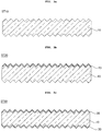
- an emitter layer 20 is formed at the front surface of the semiconductor substrate 10 by ion-implanting a first conductive type dopant. More specifically, as shown in FIG. 4 , the first conductive type dopant is ion-implanted by an ion-selection using a mass spectrometer 220.
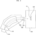
- FIG. 4 is a schematic diagram for illustrating an example of an ion-implantation apparatus used in a step of forming the emitter layer in the method of manufacturing the solar cell according to an embodiment of the invention.
- the elements not directly related to the embodiment for example, a deflector, an accelerator, and so on will not shown in FIG. 4 and not be further described.
- the invention is not limited thereto.
- various elements may be applied to the ion-implantation apparatus.
- the ion-implantation apparatus 200 includes an ion source 210 supplying ion corresponding to the ion-implanted dopant, a mass spectrometer 220 for performing an ion-selection by a mass spectrometry of an ion beam 212 supplied by the ion source 210, and an ion-implantation chamber 230 where the ion-implantation is performed.
- the ion source 210 may be an ion supplier of known structure and may be driven by one of the known methods.
- the mass spectrometer 220 may include a mass spectrometry magnet 222 providing magnetic field to the ion beam 212 and a mass spectrometry slit 224 having passages where only the predetermined ion passes through.
- a semiconductor substrate 10 is fixed to a holder 232 in the ion-implantation chamber 230 in order for the ion passing through the mass spectrometry slit 224 to implant to the semiconductor substrate 10.
- the holder 232 may move up and down and/or left and right, and one of known structures may be applied for the movement.
- a mass spectrometry of the ion beam 212 supplied from the ion source 210 is performed by the mass spectrometry magnet 222 and the mass spectrometry slit 224.
- the first conductive type dopant which is used for the ion-implantation among the ion beam 212, travels the path that is formed by the mass spectrometry magnet 222 (refer to a dotted line of FIG. 4 ) and able to pass through the mass spectrometry slit 224.
- the first conductive type dopant having atomic weight of a predetermined range pass through the mass spectrometry slit 224 only.
- the ion which is not used for the ion-implantation among the ion beam 212, travels the path that is formed by the mass spectrometry magnet 222 (refer to an alternated long and short dash line of FIG.
- the first conductive type dopant which is used for the ion-implantation among the ion beam 212, is ion-selected and passes through the mass spectrometry slit 224.
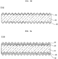
- the ion passing through the mass spectrometry slit 224 is implanted to the semiconductor substrate 10, thereby forming the emitter layer 20 at the semiconductor substrate 10, as shown in FIG. 3b .
- the dose of the hydrogen may be about 5X10 13 atoms/cm 2 or less.
- a back surface field layer 30 is formed at the back surface of the semiconductor substrate 10 by ion-implanting a second conductive type dopant.
- the second conductive type dopant for forming the back surface field layer 30 is ion-implanted without the ion-selection that uses the mass spectrometer.
- an amount of the additional dopant in the back surface field layer 30 is larger than an amount of the additional dopant in emitter layer 20.
- the additional dopant may include hydrogen, and the dose of the hydrogen may be about 1X10 14 ⁇ 5X10 15 atoms/cm 2 in the step ST30 for forming the back surface field layer.
- the additional dopant may further include at least one additional material selected from the group including potassium (K), calcium (Ca), chrome (Cr), manganese (Mn), iron (Fe), nickel (Ni), and copper (Cu).
- the ion-selection using the mass spectrometer is not performed. Accordingly, the contact resistance with the second electrode 34 can be reduced while maintaining the other properties of the solar cell 100. Also, the mass spectrometer is not used, and thus, the manufacturing cost can be reduced.
- the back surface field layer 30 is formed after the emitter layer 20 is formed.
- the invention is not limited thereto.
- the emitter layer 20 can be formed after the back surface field layer 30 is formed.
- the first conductive type dopant ion-implanted for forming the emitter layer 20 and the second conductive type dopant ion-implanted for forming the back surface field layer 30 are activated by annealing the semiconductor substrate 10.
- the first and second conductive type dopants When the first and second conductive type dopants are ion-implanted to the semiconductor substrate 10, the first and second conductive type dopants are not activated since the dopant are not positioned at the lattice sites.
- the first and second conductive type dopants of the emitter layer 20 and the back surface field layer 30 move to the lattice sites and are activated. Also, the first and second conductive type dopants diffuse into the inside of the semiconductor substrate 10.
- the heat-treating processes for activating the first and second conductive type dopants may be performed simultaneously or sequentially.
- the process can be simplified.
- the temperature and the other conditions may be varied according to materials of the first and second conductive type dopants and the semiconductor substrate 10.
- the temperature may be about 950 ⁇ 1300°C.
- the invention is not limited thereto.
- the hydrogen concentration in the back surface field layer 30 after the heat-treating at step ST40 may decrease, compared with before the heat treating at step ST40. Accordingly, the solar cell 100 is not deteriorated. In this case, the hydrogen concentration in the back surface field layer 30 is higher than hydrogen concentration in the emitter layer 20.
- a portion of the back surface field layer 30 apart from the back surface of the semiconductor substrate 10 by about 0.1 ⁇ 0.4 ⁇ m may include a region having the hydrogen concentration in a range of about 1X10 18 ⁇ 1X10 20 atoms/cm 3 .
- a portion of the emitter layer 20 apart from the front surface of the semiconductor substrate 10 by about 0.1 ⁇ 0.4 ⁇ m may include a region having the hydrogen concentration in a range of about 1X10 15 ⁇ 9X10 17 atoms/cm 3 .
- the invention is not limited thereto.
- the hydrogen concentration in the back surface field layer 30 may fall to a level similar to the hydrogen concentration in the emitter layer 20.
- the additional material such as potassium, calcium, chrome, manganese, iron, nickel, and copper may be included to a ND (not-detected) level that is regarded as "not included". That is, the additional material such as potassium, calcium, chrome, manganese, iron, nickel, and copper is not detected. Thus, the other properties of the solar cell 100 can be maintained.
- the anti-reflection film 22 and the passivation film 32 are formed on the front surface and the back surface of the semiconductor substrate 10, respectively.
- the anti-reflection film 22 and the passivation film 32 may be formed by one or more of various methods such as a vacuum evaporation, a chemical vapor deposition, a spin coating, a screen printing, or a spray coating.
- a first electrode 24 electrically connected to the emitter layer 20 is formed at the front surface of the semiconductor substrate 10 and a second electrode 34 electrically connected to the back surface field layer 30 (or, the semiconductor substrate 10) is formed at the back surface of the semiconductor substrate 10.
- the first electrode 24 may be formed inside the opening by one or more of various methods, such as a plating method or a deposition method.
- the second electrode 34 may be formed inside the opening by one or more of various methods, such as a plating method or a deposition method.
- the first and second electrodes 24 and 34 may be formed by fire-through or laser firing contact of printed pastes for the first and second electrodes 24 and 34.
- the pastes may be printed by one or more of various methods such as a screen printing method. In this case, because the openings are naturally formed during the fire-through or the laser firing contact, the steps for forming the openings are not necessary.
- each of the emitter layer 20 and the back surface field layer 30 has uniform doping concentration.
- the invention is not limited thereto.
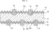
- At least one of the emitter layer 20 and the back surface field layer 30 may have a selective structure.
- the emitter layer 20 includes a first portion 20a formed adjacent to the anti-reflection film 22 between the front electrode 24, and a second portion 20b being in contact with the front electrode 24.
- the second portion 20b has a doping concentration higher than that of the first portion 20a, and thus, the second portion 20b has a resistance lower than that of the first portion 20a.
- a shallow emitter can be achieved at the first portion 20a where the sunlight is incident, and thereby enhancing the efficiency of the solar cell 100.
- contact resistance with the front electrode 24 can be reduced at the second portion 20b being in contact with the front electrode 24. That is, when the emitter layer 20 has the selective emitter structure, the efficiency of the solar cell 100 can be maximized.
- the back surface field layer 30 includes a first portion 30a formed at a portion corresponding to a portion between the back electrode 34, and a second portion 30b being in contact with the back electrode 34.
- the second portion 30b has a doping concentration higher than that of the first portion 30a, and thus, the second portion 30b has a resistance lower than that of the first portion 30a.
- the first portion 30a of the back surface field layer 30 effectively prevents the recombination of the electrons and the holes, and the contact resistance with the back electrode 34 can be reduced by the second portion 30b having a relatively low resistance. Therefore, the loss by the recombination of the electrons and the holes is reduced, and the electrons or the holes generated by the photoelectric effect can be effectively transferred to the back electrode 34. Accordingly, the efficiency of the solar cell 100 can be improved more.
- the emitter layer 20 and the back surface field layer 30 having the selective structures may be formed by one or more of various methods.
- a comb mask may be used so that the second portions 20b and 30b have a relatively high doping concentration and the first portions 20a and 30a have a relatively low doping concentration.
- the emitter layer 20 and the back surface field layer 30 having the selective structures may be formed by additionally doping the dopant only to the second portions 20b and 30b.
- An n-type semiconductor substrate was prepared. Boron as a p-type dopant was ion-implanted to a front surface of the semiconductor substrate to form an emitter layer, and phosphorus as a n-type dopant was ion-implanted to a back surface of the semiconductor substrate to form a back surface field layer. A co-activation was performed by annealing the semiconductor substrate at 1000°C. Here, an ion-selection using a mass spectrometer was performed during the ion-implantation forming the emitter layer; however, the ion-selection using the mass spectrometer was not performed during the ion-implantation forming the back surface field layer.
- An anti-reflection film was formed on the front surface of the semiconductor substrate, and a passivation film was formed on the back surface of the semiconductor substrate. Then, a first electrode electrically connected to the emitter layer and a second electrode electrically connected to the back surface field layer were formed, and a solar cell was manufactured.
- a solar cell was manufactured by the same method in Experimental Embodiment except that an ion-selection was performed in the ion-implantation for forming the back surface field layer.
- a dose of the additional dopant (hydrogen) during the ion-implantation for forming the back surface field layer in Experimental Embodiment and Comparative Example are shown in Table 1.
- Phosphorous concentration and hydrogen concentration with respect to a depth from a surface of a semiconductor substrate of a solar cell manufactured by Experimental Embodiment and Comparative Example are shown in FIG. 6 and 7 , respectively.
- the additional materials were detected by a total reflection X-ray fluorescence spectrometer after the heat-treating in Experimental Embodiment, and the result is shown in Table 2.
- the dose of the additional dopant in Experimental Embodiment is larger than that in Comparative Example.
- a portion of the back surface field layer apart from the surface of the semiconductor substrate by about 0.1 ⁇ 0.4 ⁇ m may include an region having the hydrogen concentration in a range of about 1X10 18 ⁇ 1X10 20 atoms/cm 3 .
- the contact resistance with the second electrode can be reduced and the other properties of the back surface field layer can be maintained.
- the hydrogen concentration in the back surface field layer is in a range about 1X10 17 atoms/cm 3 . That is, it can be seen that the hydrogen concentration in the back surface field layer in Comparative Example is low.
- an additional material such as potassium, calcium, and so on is not detected at the back surface field layer in Experimental Embodiment. That is, the solar cell according to Experimental Embodiment does not deteriorate and the other properties are maintained.
- the concentration of the additional dopant in the back surface field layer is higher than the concentration of the additional dopant in the emitter layer. And thus, the contact resistance of the back surface field layer with the second electrode can be increased by the additional dopant of the back surface field layer, while maintaining the other properties of the solar cell.
- the mass spectrometer is not used during the ion-implantation for forming the back surface field layer, the manufacturing cost can be effectively reduced.
Landscapes
- Photovoltaic Devices (AREA)
- Life Sciences & Earth Sciences (AREA)
- Chemical & Material Sciences (AREA)
- Crystallography & Structural Chemistry (AREA)
- Sustainable Development (AREA)
Claims (8)
- Procédé de fabrication d'une cellule solaire, comprenant les étapes consistant à :former une couche émettrice (20) par implantation avec des ions d'un premier dopant de type conducteur dans une première surface d'un substrat (10) semiconducteur ; etformer une couche de champ à surface arrière (30) par implantation avec des ions d'un second dopant de type conducteur dans une seconde surface du substrat semiconducteur,doper à l'aide d'un dopant supplémentaire, le dopant supplémentaire étant un dopant autre que le premier et le second dopant de type conducteur, une quantité de dopant supplémentaire dopé pendant la formation de la couche de champ à surface arrière étant supérieure à une quantité du dopant supplémentaire dopé pendant la formation de la couche émettrice, etle dopant supplémentaire comprenant de l'hydrogène,le procédé étant caractérisé en ce quele premier dopant de type conducteur étant implanté avec des ions par une sélection ionique à l'aide d'un spectromètre de masse dans la formation de la couche émettrice, etle second dopant de type conducteur étant implanté avec des ions sans que la section ionique n'utilise le spectromètre de masse dans la formation de la couche de champ à surface arrière.
- Procédé selon la revendication 1, une dose de l'hydrogène étant dans une plage comprise environ entre 1X10¹⁴ ∼5X10¹⁵ atomes/cm2 dans la formation de la couche de champ à surface arrière.
- Procédé selon la revendication 1, le dopant supplémentaire comprenant au moins un matériau supplémentaire sélectionné dans le groupe constitué de potassium (K), de calcium (Ca), de chrome (Cr), de manganèse (Mn), de fer (Fe), de nickel (Ni) et de cuivre (Cu).
- Procédé selon la revendication 1, comprenant en outre :
le traitement thermique pour un activation après la formation de la couche émettrice et la formation de la couche de champ à surface arrière. - Procédé selon la revendication 4, la concentration en hydrogène dans la couche de champ à surface arrière après le traitement thermique étant supérieure à la concentration en hydrogène dans la couche émettrice après le traitement thermique.
- Procédé selon la revendication 5, la concentration en hydrogène dans la couche de champ à surface arrière après le traitement thermique étant inférieure à la concentration en hydrogène dans la couche de champ à surface arrière avant le traitement thermique.
- Procédé selon la revendication 5, le dopant supplémentaire comprenant au moins un matériau supplémentaire sélectionné parmi le groupe comprenant du potassium, du calcium, du chrome, du manganèse, du fer, du nickel et du cuivre, la concentration du matériau supplémentaire dans la couche de champ à surface arrière après le traitement thermique étant inférieure à la concentration du matériau supplémentaire dans la couche de champ à surface arrière avant le traitement thermique.
- Procédé selon la revendication 1, la concentration du second dopant de type conducteur dans la couche de champ à surface arrière étant supérieure à la concentration du premier dopant de type conducteur dans la couche émettrice.
Applications Claiming Priority (1)
| Application Number | Priority Date | Filing Date | Title |
|---|---|---|---|
| KR1020120022456A KR101832230B1 (ko) | 2012-03-05 | 2012-03-05 | 태양 전지 및 이의 제조 방법 |
Publications (2)
| Publication Number | Publication Date |
|---|---|
| EP2637220A1 EP2637220A1 (fr) | 2013-09-11 |
| EP2637220B1 true EP2637220B1 (fr) | 2019-04-03 |
Family
ID=47749605
Family Applications (1)
| Application Number | Title | Priority Date | Filing Date |
|---|---|---|---|
| EP13000835.2A Active EP2637220B1 (fr) | 2012-03-05 | 2013-02-19 | Procédé de fabrication d'une cellule solaire |
Country Status (3)
| Country | Link |
|---|---|
| US (1) | US10355158B2 (fr) |
| EP (1) | EP2637220B1 (fr) |
| KR (1) | KR101832230B1 (fr) |
Families Citing this family (2)
| Publication number | Priority date | Publication date | Assignee | Title |
|---|---|---|---|---|
| KR20150035189A (ko) | 2013-09-27 | 2015-04-06 | 엘지전자 주식회사 | 태양 전지 |
| HUE046935T2 (hu) * | 2014-01-31 | 2020-03-30 | Flisom Ag | Eljárás átmenõ furat szakaszok kialakítására egy vékonyréteges fotovoltaikus eszközben |
Citations (1)
| Publication number | Priority date | Publication date | Assignee | Title |
|---|---|---|---|---|
| US20090117680A1 (en) * | 2007-11-01 | 2009-05-07 | Shunpei Yamazaki | Method for manufacturing photoelectric conversion device |
Family Cites Families (9)
| Publication number | Priority date | Publication date | Assignee | Title |
|---|---|---|---|---|
| JPS58164134A (ja) | 1982-03-24 | 1983-09-29 | Hitachi Ltd | 半導体装置の製造方法 |
| JPS6065528A (ja) | 1983-09-21 | 1985-04-15 | Hitachi Ltd | pn接合形成法 |
| KR101608953B1 (ko) | 2007-11-09 | 2016-04-04 | 가부시키가이샤 한도오따이 에네루기 켄큐쇼 | 광전 변환 장치 및 그 제조 방법 |
| EP2075850A3 (fr) | 2007-12-28 | 2011-08-24 | Semiconductor Energy Laboratory Co, Ltd. | Dispositif de conversion photoélectrique et son procédé de fabrication |
| KR101484620B1 (ko) | 2008-02-04 | 2015-01-21 | 엘지전자 주식회사 | 실리콘 태양전지 |
| US7727866B2 (en) | 2008-03-05 | 2010-06-01 | Varian Semiconductor Equipment Associates, Inc. | Use of chained implants in solar cells |
| EP2105972A3 (fr) * | 2008-03-28 | 2015-06-10 | Semiconductor Energy Laboratory Co, Ltd. | Dispositif de conversion photoélectrique et procédé de fabrication de celui-ci |
| KR101729304B1 (ko) * | 2010-12-21 | 2017-04-21 | 엘지전자 주식회사 | 태양 전지 및 그 제조 방법 |
| KR101198438B1 (ko) | 2010-12-31 | 2012-11-06 | 현대중공업 주식회사 | 양면 수광형 국부화 에미터 태양전지 및 그 제조 방법 |
-
2012
- 2012-03-05 KR KR1020120022456A patent/KR101832230B1/ko active Active
- 2012-10-09 US US13/647,920 patent/US10355158B2/en active Active
-
2013
- 2013-02-19 EP EP13000835.2A patent/EP2637220B1/fr active Active
Patent Citations (1)
| Publication number | Priority date | Publication date | Assignee | Title |
|---|---|---|---|---|
| US20090117680A1 (en) * | 2007-11-01 | 2009-05-07 | Shunpei Yamazaki | Method for manufacturing photoelectric conversion device |
Non-Patent Citations (2)
| Title |
|---|
| TAHARA Y ET AL: "HIGH THROUGHPUT AUTOMATED JUNCTION FORMATION BY ION IMPLANTATION AND HALOGEN LAMP ANNEAL FOR 9MW PRODUCTION", PHOTOVOLTAIC SPECIALISTS CONFERENCE. LAS VEGAS, OCT. 21 - 25, 1985; [PHOTOVOLTAIC SPECIALISTS CONFERENCE], NEW YORK, IEEE, US, vol. CONF. 18, 21 October 1985 (1985-10-21), pages 792 - 796, XP000132062 * |
| WESTBROOK R D ET AL: "GLOW-DISCHARGE-IMPLANTED, THERMALLY ANNEALED, OXIDE-PASSIVATED SILICON SOLAR CELLS OF 19% EFFICIENCY", APPLIED PHYSICS LETTERS, A I P PUBLISHING LLC, US, vol. 50, no. 8, 23 February 1987 (1987-02-23), pages 469 - 471, XP000816298, ISSN: 0003-6951, DOI: 10.1063/1.98176 * |
Also Published As
| Publication number | Publication date |
|---|---|
| KR20130101364A (ko) | 2013-09-13 |
| EP2637220A1 (fr) | 2013-09-11 |
| KR101832230B1 (ko) | 2018-04-13 |
| US10355158B2 (en) | 2019-07-16 |
| US20130228215A1 (en) | 2013-09-05 |
Similar Documents
| Publication | Publication Date | Title |
|---|---|---|
| EP2654090B1 (fr) | Cellule solaire | |
| US9978888B2 (en) | Solar cell and method for manufacturing the same | |
| EP2608280B1 (fr) | Procédé de fabrication d'une cellule solaire comprenant une implantation ionique et l'activation sélective de régions d'émetteur et de BSF par traitement au laser | |
| US9515212B2 (en) | Solar cell and method for manufacturing with pre-amorphization implant to form emitter | |
| EP2677546B1 (fr) | Procédé de fabrication de cellule solaire et sa couche de dopant | |
| EP2662904B1 (fr) | Procédé de fabrication de cellule solaire | |
| EP2637220B1 (fr) | Procédé de fabrication d'une cellule solaire | |
| KR20140140201A (ko) | 태양 전지의 제조 방법 및 불순물 영역의 형성 방법 | |
| US9293623B2 (en) | Techniques for manufacturing devices | |
| KR20130117095A (ko) | 태양 전지 및 이의 제조 방법 | |
| KR101807791B1 (ko) | 태양 전지의 제조 방법 | |
| KR101916436B1 (ko) | 태양 전지의 제조 방법 | |
| KR101788012B1 (ko) | 태양전지의 제조방법 |
Legal Events
| Date | Code | Title | Description |
|---|---|---|---|
| PUAI | Public reference made under article 153(3) epc to a published international application that has entered the european phase |
Free format text: ORIGINAL CODE: 0009012 |
|
| 17P | Request for examination filed |
Effective date: 20130219 |
|
| AK | Designated contracting states |
Kind code of ref document: A1 Designated state(s): AL AT BE BG CH CY CZ DE DK EE ES FI FR GB GR HR HU IE IS IT LI LT LU LV MC MK MT NL NO PL PT RO RS SE SI SK SM TR |
|
| AX | Request for extension of the european patent |
Extension state: BA ME |
|
| STAA | Information on the status of an ep patent application or granted ep patent |
Free format text: STATUS: EXAMINATION IS IN PROGRESS |
|
| 17Q | First examination report despatched |
Effective date: 20170503 |
|
| GRAP | Despatch of communication of intention to grant a patent |
Free format text: ORIGINAL CODE: EPIDOSNIGR1 |
|
| STAA | Information on the status of an ep patent application or granted ep patent |
Free format text: STATUS: GRANT OF PATENT IS INTENDED |
|
| INTG | Intention to grant announced |
Effective date: 20180904 |
|
| GRAS | Grant fee paid |
Free format text: ORIGINAL CODE: EPIDOSNIGR3 |
|
| GRAA | (expected) grant |
Free format text: ORIGINAL CODE: 0009210 |
|
| STAA | Information on the status of an ep patent application or granted ep patent |
Free format text: STATUS: THE PATENT HAS BEEN GRANTED |
|
| AK | Designated contracting states |
Kind code of ref document: B1 Designated state(s): AL AT BE BG CH CY CZ DE DK EE ES FI FR GB GR HR HU IE IS IT LI LT LU LV MC MK MT NL NO PL PT RO RS SE SI SK SM TR |
|
| REG | Reference to a national code |
Ref country code: GB Ref legal event code: FG4D |
|
| REG | Reference to a national code |
Ref country code: CH Ref legal event code: EP Ref country code: AT Ref legal event code: REF Ref document number: 1116793 Country of ref document: AT Kind code of ref document: T Effective date: 20190415 |
|
| REG | Reference to a national code |
Ref country code: DE Ref legal event code: R096 Ref document number: 602013053168 Country of ref document: DE |
|
| REG | Reference to a national code |
Ref country code: IE Ref legal event code: FG4D |
|
| REG | Reference to a national code |
Ref country code: NL Ref legal event code: MP Effective date: 20190403 |
|
| REG | Reference to a national code |
Ref country code: LT Ref legal event code: MG4D |
|
| REG | Reference to a national code |
Ref country code: AT Ref legal event code: MK05 Ref document number: 1116793 Country of ref document: AT Kind code of ref document: T Effective date: 20190403 |
|
| PG25 | Lapsed in a contracting state [announced via postgrant information from national office to epo] |
Ref country code: NL Free format text: LAPSE BECAUSE OF FAILURE TO SUBMIT A TRANSLATION OF THE DESCRIPTION OR TO PAY THE FEE WITHIN THE PRESCRIBED TIME-LIMIT Effective date: 20190403 |
|
| PG25 | Lapsed in a contracting state [announced via postgrant information from national office to epo] |
Ref country code: FI Free format text: LAPSE BECAUSE OF FAILURE TO SUBMIT A TRANSLATION OF THE DESCRIPTION OR TO PAY THE FEE WITHIN THE PRESCRIBED TIME-LIMIT Effective date: 20190403 Ref country code: LT Free format text: LAPSE BECAUSE OF FAILURE TO SUBMIT A TRANSLATION OF THE DESCRIPTION OR TO PAY THE FEE WITHIN THE PRESCRIBED TIME-LIMIT Effective date: 20190403 Ref country code: CZ Free format text: LAPSE BECAUSE OF FAILURE TO SUBMIT A TRANSLATION OF THE DESCRIPTION OR TO PAY THE FEE WITHIN THE PRESCRIBED TIME-LIMIT Effective date: 20190403 Ref country code: ES Free format text: LAPSE BECAUSE OF FAILURE TO SUBMIT A TRANSLATION OF THE DESCRIPTION OR TO PAY THE FEE WITHIN THE PRESCRIBED TIME-LIMIT Effective date: 20190403 Ref country code: PT Free format text: LAPSE BECAUSE OF FAILURE TO SUBMIT A TRANSLATION OF THE DESCRIPTION OR TO PAY THE FEE WITHIN THE PRESCRIBED TIME-LIMIT Effective date: 20190803 Ref country code: AL Free format text: LAPSE BECAUSE OF FAILURE TO SUBMIT A TRANSLATION OF THE DESCRIPTION OR TO PAY THE FEE WITHIN THE PRESCRIBED TIME-LIMIT Effective date: 20190403 Ref country code: HR Free format text: LAPSE BECAUSE OF FAILURE TO SUBMIT A TRANSLATION OF THE DESCRIPTION OR TO PAY THE FEE WITHIN THE PRESCRIBED TIME-LIMIT Effective date: 20190403 Ref country code: SE Free format text: LAPSE BECAUSE OF FAILURE TO SUBMIT A TRANSLATION OF THE DESCRIPTION OR TO PAY THE FEE WITHIN THE PRESCRIBED TIME-LIMIT Effective date: 20190403 Ref country code: NO Free format text: LAPSE BECAUSE OF FAILURE TO SUBMIT A TRANSLATION OF THE DESCRIPTION OR TO PAY THE FEE WITHIN THE PRESCRIBED TIME-LIMIT Effective date: 20190703 |
|
| PG25 | Lapsed in a contracting state [announced via postgrant information from national office to epo] |
Ref country code: GR Free format text: LAPSE BECAUSE OF FAILURE TO SUBMIT A TRANSLATION OF THE DESCRIPTION OR TO PAY THE FEE WITHIN THE PRESCRIBED TIME-LIMIT Effective date: 20190704 Ref country code: PL Free format text: LAPSE BECAUSE OF FAILURE TO SUBMIT A TRANSLATION OF THE DESCRIPTION OR TO PAY THE FEE WITHIN THE PRESCRIBED TIME-LIMIT Effective date: 20190403 Ref country code: LV Free format text: LAPSE BECAUSE OF FAILURE TO SUBMIT A TRANSLATION OF THE DESCRIPTION OR TO PAY THE FEE WITHIN THE PRESCRIBED TIME-LIMIT Effective date: 20190403 Ref country code: RS Free format text: LAPSE BECAUSE OF FAILURE TO SUBMIT A TRANSLATION OF THE DESCRIPTION OR TO PAY THE FEE WITHIN THE PRESCRIBED TIME-LIMIT Effective date: 20190403 Ref country code: BG Free format text: LAPSE BECAUSE OF FAILURE TO SUBMIT A TRANSLATION OF THE DESCRIPTION OR TO PAY THE FEE WITHIN THE PRESCRIBED TIME-LIMIT Effective date: 20190703 |
|
| PG25 | Lapsed in a contracting state [announced via postgrant information from national office to epo] |
Ref country code: AT Free format text: LAPSE BECAUSE OF FAILURE TO SUBMIT A TRANSLATION OF THE DESCRIPTION OR TO PAY THE FEE WITHIN THE PRESCRIBED TIME-LIMIT Effective date: 20190403 Ref country code: IS Free format text: LAPSE BECAUSE OF FAILURE TO SUBMIT A TRANSLATION OF THE DESCRIPTION OR TO PAY THE FEE WITHIN THE PRESCRIBED TIME-LIMIT Effective date: 20190803 |
|
| REG | Reference to a national code |
Ref country code: DE Ref legal event code: R097 Ref document number: 602013053168 Country of ref document: DE |
|
| PG25 | Lapsed in a contracting state [announced via postgrant information from national office to epo] |
Ref country code: RO Free format text: LAPSE BECAUSE OF FAILURE TO SUBMIT A TRANSLATION OF THE DESCRIPTION OR TO PAY THE FEE WITHIN THE PRESCRIBED TIME-LIMIT Effective date: 20190403 Ref country code: SK Free format text: LAPSE BECAUSE OF FAILURE TO SUBMIT A TRANSLATION OF THE DESCRIPTION OR TO PAY THE FEE WITHIN THE PRESCRIBED TIME-LIMIT Effective date: 20190403 Ref country code: EE Free format text: LAPSE BECAUSE OF FAILURE TO SUBMIT A TRANSLATION OF THE DESCRIPTION OR TO PAY THE FEE WITHIN THE PRESCRIBED TIME-LIMIT Effective date: 20190403 Ref country code: DK Free format text: LAPSE BECAUSE OF FAILURE TO SUBMIT A TRANSLATION OF THE DESCRIPTION OR TO PAY THE FEE WITHIN THE PRESCRIBED TIME-LIMIT Effective date: 20190403 |
|
| PLBE | No opposition filed within time limit |
Free format text: ORIGINAL CODE: 0009261 |
|
| STAA | Information on the status of an ep patent application or granted ep patent |
Free format text: STATUS: NO OPPOSITION FILED WITHIN TIME LIMIT |
|
| PG25 | Lapsed in a contracting state [announced via postgrant information from national office to epo] |
Ref country code: IT Free format text: LAPSE BECAUSE OF FAILURE TO SUBMIT A TRANSLATION OF THE DESCRIPTION OR TO PAY THE FEE WITHIN THE PRESCRIBED TIME-LIMIT Effective date: 20190403 Ref country code: SM Free format text: LAPSE BECAUSE OF FAILURE TO SUBMIT A TRANSLATION OF THE DESCRIPTION OR TO PAY THE FEE WITHIN THE PRESCRIBED TIME-LIMIT Effective date: 20190403 |
|
| 26N | No opposition filed |
Effective date: 20200106 |
|
| PG25 | Lapsed in a contracting state [announced via postgrant information from national office to epo] |
Ref country code: TR Free format text: LAPSE BECAUSE OF FAILURE TO SUBMIT A TRANSLATION OF THE DESCRIPTION OR TO PAY THE FEE WITHIN THE PRESCRIBED TIME-LIMIT Effective date: 20190403 |
|
| PG25 | Lapsed in a contracting state [announced via postgrant information from national office to epo] |
Ref country code: SI Free format text: LAPSE BECAUSE OF FAILURE TO SUBMIT A TRANSLATION OF THE DESCRIPTION OR TO PAY THE FEE WITHIN THE PRESCRIBED TIME-LIMIT Effective date: 20190403 |
|
| REG | Reference to a national code |
Ref country code: CH Ref legal event code: PL |
|
| GBPC | Gb: european patent ceased through non-payment of renewal fee |
Effective date: 20200219 |
|
| REG | Reference to a national code |
Ref country code: BE Ref legal event code: MM Effective date: 20200229 |
|
| PG25 | Lapsed in a contracting state [announced via postgrant information from national office to epo] |
Ref country code: MC Free format text: LAPSE BECAUSE OF FAILURE TO SUBMIT A TRANSLATION OF THE DESCRIPTION OR TO PAY THE FEE WITHIN THE PRESCRIBED TIME-LIMIT Effective date: 20190403 Ref country code: LU Free format text: LAPSE BECAUSE OF NON-PAYMENT OF DUE FEES Effective date: 20200219 |
|
| PG25 | Lapsed in a contracting state [announced via postgrant information from national office to epo] |
Ref country code: LI Free format text: LAPSE BECAUSE OF NON-PAYMENT OF DUE FEES Effective date: 20200229 Ref country code: CH Free format text: LAPSE BECAUSE OF NON-PAYMENT OF DUE FEES Effective date: 20200229 |
|
| PG25 | Lapsed in a contracting state [announced via postgrant information from national office to epo] |
Ref country code: FR Free format text: LAPSE BECAUSE OF NON-PAYMENT OF DUE FEES Effective date: 20200229 Ref country code: GB Free format text: LAPSE BECAUSE OF NON-PAYMENT OF DUE FEES Effective date: 20200219 Ref country code: IE Free format text: LAPSE BECAUSE OF NON-PAYMENT OF DUE FEES Effective date: 20200219 |
|
| PG25 | Lapsed in a contracting state [announced via postgrant information from national office to epo] |
Ref country code: BE Free format text: LAPSE BECAUSE OF NON-PAYMENT OF DUE FEES Effective date: 20200229 |
|
| PG25 | Lapsed in a contracting state [announced via postgrant information from national office to epo] |
Ref country code: MT Free format text: LAPSE BECAUSE OF FAILURE TO SUBMIT A TRANSLATION OF THE DESCRIPTION OR TO PAY THE FEE WITHIN THE PRESCRIBED TIME-LIMIT Effective date: 20190403 Ref country code: CY Free format text: LAPSE BECAUSE OF FAILURE TO SUBMIT A TRANSLATION OF THE DESCRIPTION OR TO PAY THE FEE WITHIN THE PRESCRIBED TIME-LIMIT Effective date: 20190403 |
|
| PG25 | Lapsed in a contracting state [announced via postgrant information from national office to epo] |
Ref country code: MK Free format text: LAPSE BECAUSE OF FAILURE TO SUBMIT A TRANSLATION OF THE DESCRIPTION OR TO PAY THE FEE WITHIN THE PRESCRIBED TIME-LIMIT Effective date: 20190403 |
|
| REG | Reference to a national code |
Ref country code: DE Ref legal event code: R081 Ref document number: 602013053168 Country of ref document: DE Owner name: SHANGRAO JINKO SOLAR TECHNOLOGY DEVELOPMENT CO, CN Free format text: FORMER OWNER: LG ELECTRONICS INC., SEOUL, KR Ref country code: DE Ref legal event code: R082 Ref document number: 602013053168 Country of ref document: DE Representative=s name: DREISS PATENTANWAELTE PARTG MBB, DE Ref country code: DE Ref legal event code: R081 Ref document number: 602013053168 Country of ref document: DE Owner name: SHANGRAO XINYUAN YUEDONG TECHNOLOGY DEVELOPMEN, CN Free format text: FORMER OWNER: LG ELECTRONICS INC., SEOUL, KR |
|
| REG | Reference to a national code |
Ref country code: DE Ref legal event code: R081 Ref document number: 602013053168 Country of ref document: DE Owner name: SHANGRAO XINYUAN YUEDONG TECHNOLOGY DEVELOPMEN, CN Free format text: FORMER OWNER: SHANGRAO JINKO SOLAR TECHNOLOGY DEVELOPMENT CO., LTD, SHANGRAO, JIANGXI PROVINCE, CN |
|
| REG | Reference to a national code |
Ref country code: DE Ref legal event code: R079 Ref document number: 602013053168 Country of ref document: DE Free format text: PREVIOUS MAIN CLASS: H01L0031068000 Ipc: H10F0010140000 |
|
| PGFP | Annual fee paid to national office [announced via postgrant information from national office to epo] |
Ref country code: DE Payment date: 20260218 Year of fee payment: 14 |