EP2637230A1 - Procédé de préparation d'un dispositif électroluminescent organique, substrat pour faire transiter une couche inorganique et dispositif électroluminescent organique - Google Patents
Procédé de préparation d'un dispositif électroluminescent organique, substrat pour faire transiter une couche inorganique et dispositif électroluminescent organique Download PDFInfo
- Publication number
- EP2637230A1 EP2637230A1 EP20120192714 EP12192714A EP2637230A1 EP 2637230 A1 EP2637230 A1 EP 2637230A1 EP 20120192714 EP20120192714 EP 20120192714 EP 12192714 A EP12192714 A EP 12192714A EP 2637230 A1 EP2637230 A1 EP 2637230A1
- Authority
- EP
- European Patent Office
- Prior art keywords
- substrate
- layer
- organic
- inorganic
- inorganic layer
- Prior art date
- Legal status (The legal status is an assumption and is not a legal conclusion. Google has not performed a legal analysis and makes no representation as to the accuracy of the status listed.)
- Granted
Links
Images







Classifications
-
- C—CHEMISTRY; METALLURGY
- C03—GLASS; MINERAL OR SLAG WOOL
- C03C—CHEMICAL COMPOSITION OF GLASSES, GLAZES OR VITREOUS ENAMELS; SURFACE TREATMENT OF GLASS; SURFACE TREATMENT OF FIBRES OR FILAMENTS MADE FROM GLASS, MINERALS OR SLAGS; JOINING GLASS TO GLASS OR OTHER MATERIALS
- C03C17/00—Surface treatment of glass, not in the form of fibres or filaments, by coating
- C03C17/34—Surface treatment of glass, not in the form of fibres or filaments, by coating with at least two coatings having different compositions
- C03C17/42—Surface treatment of glass, not in the form of fibres or filaments, by coating with at least two coatings having different compositions at least one coating of an organic material and at least one non-metal coating
-
- H—ELECTRICITY
- H10—SEMICONDUCTOR DEVICES; ELECTRIC SOLID-STATE DEVICES NOT OTHERWISE PROVIDED FOR
- H10K—ORGANIC ELECTRIC SOLID-STATE DEVICES
- H10K71/00—Manufacture or treatment specially adapted for the organic devices covered by this subclass
-
- C—CHEMISTRY; METALLURGY
- C03—GLASS; MINERAL OR SLAG WOOL
- C03C—CHEMICAL COMPOSITION OF GLASSES, GLAZES OR VITREOUS ENAMELS; SURFACE TREATMENT OF GLASS; SURFACE TREATMENT OF FIBRES OR FILAMENTS MADE FROM GLASS, MINERALS OR SLAGS; JOINING GLASS TO GLASS OR OTHER MATERIALS
- C03C27/00—Joining pieces of glass to pieces of other inorganic material; Joining glass to glass other than by fusing
- C03C27/06—Joining glass to glass by processes other than fusing
- C03C27/10—Joining glass to glass by processes other than fusing with the aid of adhesive specially adapted for that purpose
-
- H—ELECTRICITY
- H10—SEMICONDUCTOR DEVICES; ELECTRIC SOLID-STATE DEVICES NOT OTHERWISE PROVIDED FOR
- H10D—INORGANIC ELECTRIC SEMICONDUCTOR DEVICES
- H10D62/00—Semiconductor bodies, or regions thereof, of devices having potential barriers
- H10D62/10—Shapes, relative sizes or dispositions of the regions of the semiconductor bodies; Shapes of the semiconductor bodies
-
- H—ELECTRICITY
- H10—SEMICONDUCTOR DEVICES; ELECTRIC SOLID-STATE DEVICES NOT OTHERWISE PROVIDED FOR
- H10D—INORGANIC ELECTRIC SEMICONDUCTOR DEVICES
- H10D62/00—Semiconductor bodies, or regions thereof, of devices having potential barriers
- H10D62/10—Shapes, relative sizes or dispositions of the regions of the semiconductor bodies; Shapes of the semiconductor bodies
- H10D62/13—Semiconductor regions connected to electrodes carrying current to be rectified, amplified or switched, e.g. source or drain regions
-
- H—ELECTRICITY
- H10—SEMICONDUCTOR DEVICES; ELECTRIC SOLID-STATE DEVICES NOT OTHERWISE PROVIDED FOR
- H10H—INORGANIC LIGHT-EMITTING SEMICONDUCTOR DEVICES HAVING POTENTIAL BARRIERS
- H10H29/00—Integrated devices, or assemblies of multiple devices, comprising at least one light-emitting semiconductor element covered by group H10H20/00
- H10H29/10—Integrated devices comprising at least one light-emitting semiconductor component covered by group H10H20/00
-
- H—ELECTRICITY
- H10—SEMICONDUCTOR DEVICES; ELECTRIC SOLID-STATE DEVICES NOT OTHERWISE PROVIDED FOR
- H10K—ORGANIC ELECTRIC SOLID-STATE DEVICES
- H10K50/00—Organic light-emitting devices
- H10K50/80—Constructional details
- H10K50/805—Electrodes
-
- H—ELECTRICITY
- H10—SEMICONDUCTOR DEVICES; ELECTRIC SOLID-STATE DEVICES NOT OTHERWISE PROVIDED FOR
- H10K—ORGANIC ELECTRIC SOLID-STATE DEVICES
- H10K50/00—Organic light-emitting devices
- H10K50/80—Constructional details
- H10K50/84—Passivation; Containers; Encapsulations
- H10K50/844—Encapsulations
-
- H—ELECTRICITY
- H10—SEMICONDUCTOR DEVICES; ELECTRIC SOLID-STATE DEVICES NOT OTHERWISE PROVIDED FOR
- H10K—ORGANIC ELECTRIC SOLID-STATE DEVICES
- H10K50/00—Organic light-emitting devices
- H10K50/80—Constructional details
- H10K50/84—Passivation; Containers; Encapsulations
- H10K50/844—Encapsulations
- H10K50/8445—Encapsulations multilayered coatings having a repetitive structure, e.g. having multiple organic-inorganic bilayers
-
- H—ELECTRICITY
- H10—SEMICONDUCTOR DEVICES; ELECTRIC SOLID-STATE DEVICES NOT OTHERWISE PROVIDED FOR
- H10K—ORGANIC ELECTRIC SOLID-STATE DEVICES
- H10K77/00—Constructional details of devices covered by this subclass and not covered by groups H10K10/80, H10K30/80, H10K50/80 or H10K59/80
- H10K77/10—Substrates, e.g. flexible substrates
-
- C—CHEMISTRY; METALLURGY
- C03—GLASS; MINERAL OR SLAG WOOL
- C03C—CHEMICAL COMPOSITION OF GLASSES, GLAZES OR VITREOUS ENAMELS; SURFACE TREATMENT OF GLASS; SURFACE TREATMENT OF FIBRES OR FILAMENTS MADE FROM GLASS, MINERALS OR SLAGS; JOINING GLASS TO GLASS OR OTHER MATERIALS
- C03C2218/00—Methods for coating glass
- C03C2218/30—Aspects of methods for coating glass not covered above
- C03C2218/34—Masking
-
- H—ELECTRICITY
- H10—SEMICONDUCTOR DEVICES; ELECTRIC SOLID-STATE DEVICES NOT OTHERWISE PROVIDED FOR
- H10K—ORGANIC ELECTRIC SOLID-STATE DEVICES
- H10K50/00—Organic light-emitting devices
- H10K50/80—Constructional details
- H10K50/805—Electrodes
- H10K50/81—Anodes
- H10K50/816—Multilayers, e.g. transparent multilayers
-
- H—ELECTRICITY
- H10—SEMICONDUCTOR DEVICES; ELECTRIC SOLID-STATE DEVICES NOT OTHERWISE PROVIDED FOR
- H10K—ORGANIC ELECTRIC SOLID-STATE DEVICES
- H10K71/00—Manufacture or treatment specially adapted for the organic devices covered by this subclass
- H10K71/40—Thermal treatment, e.g. annealing in the presence of a solvent vapour
- H10K71/421—Thermal treatment, e.g. annealing in the presence of a solvent vapour using coherent electromagnetic radiation, e.g. laser annealing
-
- Y—GENERAL TAGGING OF NEW TECHNOLOGICAL DEVELOPMENTS; GENERAL TAGGING OF CROSS-SECTIONAL TECHNOLOGIES SPANNING OVER SEVERAL SECTIONS OF THE IPC; TECHNICAL SUBJECTS COVERED BY FORMER USPC CROSS-REFERENCE ART COLLECTIONS [XRACs] AND DIGESTS
- Y02—TECHNOLOGIES OR APPLICATIONS FOR MITIGATION OR ADAPTATION AGAINST CLIMATE CHANGE
- Y02E—REDUCTION OF GREENHOUSE GAS [GHG] EMISSIONS, RELATED TO ENERGY GENERATION, TRANSMISSION OR DISTRIBUTION
- Y02E10/00—Energy generation through renewable energy sources
- Y02E10/50—Photovoltaic [PV] energy
- Y02E10/549—Organic PV cells
-
- Y—GENERAL TAGGING OF NEW TECHNOLOGICAL DEVELOPMENTS; GENERAL TAGGING OF CROSS-SECTIONAL TECHNOLOGIES SPANNING OVER SEVERAL SECTIONS OF THE IPC; TECHNICAL SUBJECTS COVERED BY FORMER USPC CROSS-REFERENCE ART COLLECTIONS [XRACs] AND DIGESTS
- Y10—TECHNICAL SUBJECTS COVERED BY FORMER USPC
- Y10T—TECHNICAL SUBJECTS COVERED BY FORMER US CLASSIFICATION
- Y10T156/00—Adhesive bonding and miscellaneous chemical manufacture
- Y10T156/10—Methods of surface bonding and/or assembly therefor
-
- Y—GENERAL TAGGING OF NEW TECHNOLOGICAL DEVELOPMENTS; GENERAL TAGGING OF CROSS-SECTIONAL TECHNOLOGIES SPANNING OVER SEVERAL SECTIONS OF THE IPC; TECHNICAL SUBJECTS COVERED BY FORMER USPC CROSS-REFERENCE ART COLLECTIONS [XRACs] AND DIGESTS
- Y10—TECHNICAL SUBJECTS COVERED BY FORMER USPC
- Y10T—TECHNICAL SUBJECTS COVERED BY FORMER US CLASSIFICATION
- Y10T428/00—Stock material or miscellaneous articles
- Y10T428/31504—Composite [nonstructural laminate]
- Y10T428/31678—Of metal
Definitions
- the present invention relates to a method of preparing an organic light-emitting device, a substrate for transiting an inorganic layer, and an organic light-emitting device.
- Organic light emitting devices which are self-emitting devices, have advantages such as a wide viewing angle, excellent contrast, quick response, high brightness, excellent driving voltage characteristics, and can display multicolored images.
- the organic light-emitting device includes an organic emission unit including a first electrode, an organic layer, and a second electrode. Since the organic emission unit is vulnerable to an external environment, for example, oxygen and moisture, a sealing structure that seals the organic emission unit from the external environment is used.
- a method of preparing an organic light-emitting device including: forming at least one pre-inorganic layer including a low temperature viscosity transition (LVT) inorganic material on a second substrate; forming at least one organic emission unit on a first substrate; applying an adhesive to edge portions of at least one of the second substrate or the first substrate; bonding the second substrate and the first substrate using the adhesive such that the pre-inorganic layer and the organic emission unit face each other; and transiting the pre-inorganic layer to an inorganic layer to cover the organic emission unit by performing a healing process on the pre-inorganic layer at a temperature greater than a viscosity transition temperature of the LVT inorganic material.
- LVT low temperature viscosity transition
- the method may further include separating the inorganic layer from the second substrate.
- the second substrate may include glass, plastic, or metal.
- the forming of the organic layer and/or the forming of the first organic layer may include providing a curable precursor, and curing the curable precursor.
- the providing of the curable precursor may be performed by using a flash evaporator.
- the curing of the curable precursor may be performed by using UV rays, infrared rays, and laser beams.
- the forming of the pre-inorganic layer may include: applying a paste including a powder of the LVT inorganic material to the second substrate; and sintering the paste.
- the forming of the pre-inorganic layer may include: applying a dispersion including a powder of the LVT inorganic material to the second substrate by spraying; and heat-treating the dispersion.
- the bonding of the second substrate and the first substrate may be performed in a vacuum, under a reduced pressure, or in an inert atmosphere in which an influence of moisture or oxygen is substantially eliminated so that the space between the second substrate and the first substrate is substantially maintained in a vacuum.
- the viscosity transition temperature of the LVT inorganic material may be a minimum temperature capable of providing fluidity to the LVT inorganic material.
- the viscosity transition temperature of the LVT inorganic material may be less than a minimum value of denaturation temperatures of materials contained in the organic emission unit.
- the LVT inorganic material may include a tin oxide.
- the LVT inorganic material may include at least one selected from the group consisting of a phosphorus oxide, a boron phosphate, a tin fluoride, a niobium oxide, and a tungsten oxide.
- the LVT inorganic material may include SnO; SnO and P 2 O 5 ; SnO and BPO 4 ; SnO, SnF 2 , and P 2 O 5 ; SnO, SnF 2 , P 2 O 5 , and NbO; or SnO, SnF 2 , P 2 O 5 , and WO 3 .
- the transiting may be performed by heat-treating the pre-inorganic layer at a temperature between the viscosity transition temperature of the LVT inorganic material and a minimum value of denaturation temperatures of materials contained in the organic emission layer.
- the transiting may include heat-treating the pre-inorganic layer at a temperature between about 80°C and about 132°C for about 1 to 3 hours.
- the transiting may be performed in a vacuum or in an inert gas atmosphere.
- the transiting may include scanning the pre-inorganic layer while irradiating the pre-inorganic layer with a laser beam.
- the method may further include forming at least one second organic layer between the second substrate and the pre-inorganic layer.
- the separating the inorganic layer from the second substrate may include separating the second organic layer from the second substrate by irradiating the second organic layer with a laser beam.
- the second organic layer may cover at least one portion of the inorganic layer.
- a substrate for transiting an inorganic layer including: a substrate; and at least one inorganic layer formed on one surface of the substrate and including a low temperature viscosity transition (LVT) inorganic material.
- LVT low temperature viscosity transition
- the substrate may further include at least one organic layer between the inorganic layer and the substrate.
- the organic layer may include a heat-resistant organic material.
- the viscosity transition temperature of the LVT inorganic material may be a minimum temperature capable of providing fluidity to the LVT inorganic material.
- the LVT inorganic material may include a tin oxide.
- the LVT inorganic material may include at least one selected from the group consisting of a phosphorus oxide, a boron phosphate, a tin fluoride, a niobium oxide, and a tungsten oxide.
- the LVT inorganic material may include SnO; SnO and P 2 O 5 ; SnO, and BPO 4 ; SnO, SnF 2 , and P 2 O 5 ; SnO, SnF 2 , P 2 O 5 , and NbO; or SnO, SnF 2 , P 2 O 5 , and WO 3 .
- the second substrate may include glass, plastic, or metal.
- an organic light-emitting device including: a first substrate; an organic emission unit on one surface of the first substrate; an inorganic layer including a low temperature viscosity transition (LVT) inorganic material and covering the organic emission unit; and a second substrate on the inorganic layer facing the first substrate.
- LVT low temperature viscosity transition
- the organic light-emitting device may further include a first organic layer between the inorganic layer and the organic emission unit.
- the inorganic layer may be transited onto the organic emission unit to cover the organic emission unit.
- the organic light-emitting device may further include a second organic layer between the second substrate and the inorganic layer.
- the organic light-emitting device may further include an adhesive between the first substrate and the second substrate and disposed outside of the organic emission unit.
- the viscosity transition temperature of the LVT inorganic material may be a minimum temperature capable of providing fluidity to the LVT inorganic material.
- the LVT inorganic material may include a tin oxide.
- the LVT inorganic material may include at least one selected from the group consisting of a phosphorus oxide, a boron phosphate, a tin fluoride, a niobium oxide, and a tungsten oxide.
- the LVT inorganic material may include SnO; SnO and P 2 O 5 ; SnO, and BPO 4 ; SnO, SnF 2 , and P 2 O 5 ; SnO, SnF 2 , P 2 O 5 , and NbO; or SnO, SnF 2 , P 2 O 5 , and WO 3 .
- the second substrate may include glass, plastic, or metal.
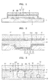
- FIG. 1 is a schematic cross-sectional view of an organic light-emitting device according to an embodiment of the present invention
- FIG. 2 is a cross-sectional view of a portion II of FIG. 1 ;
- FIG. 3 is a cross-sectional view of a portion III of FIG. 1 ;
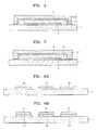
- FIG. 4 is a schematic cross-sectional view of an organic light-emitting device according to another embodiment of the present invention.
- FIG. 5 is a schematic cross-sectional view of an organic light-emitting device according to another embodiment of the present invention.
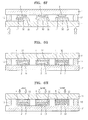
- FIGS. 6A through 6J are diagrams for describing a method of preparing the organic light-emitting device of FIG. 1 ;
- FIG. 7 is a schematic cross-sectional view of an organic light-emitting device according to another embodiment of the present invention.
- FIG. 8 is a schematic cross-sectional view of an organic light-emitting device according to another embodiment of the present invention.
- FIG. 9 is a schematic cross-sectional view of an organic light-emitting device according to another embodiment of the present invention.
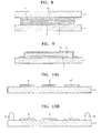
- FIGS. 10A through 10H are diagrams for describing a method of preparing the organic light-emitting device of FIG. 9 ;
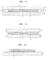
- FIG. 11 is a schematic cross-sectional view of an organic light-emitting device according to another embodiment of the present invention.
- FIG. 12 is a schematic cross-sectional view of an organic light-emitting device according to another embodiment of the present invention.
- FIG. 13 is a schematic cross-sectional view of an organic light-emitting device according to another embodiment of the present invention.
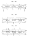
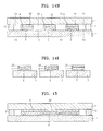
- FIGS. 14A through 14I are diagrams for describing a method of preparing the organic light-emitting device of FIG. 13 ;
- FIG. 15 is a schematic cross-sectional view of an organic light-emitting device according to another embodiment of the present invention.
- FIG. 16 is a schematic cross-sectional view of an organic light-emitting device according to another embodiment of the present invention.
- FIG. 17 is a schematic cross-sectional view of an organic light-emitting device according to another embodiment of the present invention.
- FIGS. 18A through 18H are diagrams for describing a method of preparing the organic light-emitting device of FIG. 17 ;
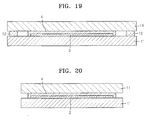
- FIG. 19 is a schematic cross-sectional view of an organic light-emitting device according to another embodiment of the present invention.
- FIG. 20 is a schematic cross-sectional view of an organic light-emitting device according to another embodiment of the present invention.
- FIG. 1 is a schematic cross-sectional view of an organic light-emitting device according to an embodiment of the present invention.
- FIG. 2 is a cross-sectional view of a portion II of FIG. 1
- FIG. 3 is a cross-sectional view of a portion III of FIG. 1 .
- an organic emission unit 2 is formed on one surface of a first substrate 1, a laminate of an organic layer 3 and an inorganic layer 4, is formed on the first substrate 1 such that the laminate covers the organic emission unit 2.
- the first substrate 1 may be formed of glass, but is not limited thereto.
- the first substrate 1 may also be formed of metal or plastic.
- the first substrate 1 may be a flexible substrate that is bendable. In one embodiment, a bending radius of the first substrate 1 is 10 cm or less.
- the organic emission unit 2 formed on the first substrate 1 includes a laminate including a first electrode 21, a second electrode 22, and an organic emission layer 23 interposed between the first electrode 21 and the second electrode 22 as shown in FIG. 2 .
- the organic emission unit 2 includes a plurality of pixels and one pixel circuit per pixel, and the pixel circuit includes at least one thin film transistor (TFT) (not shown) and a capacitor (not shown).
- TFT thin film transistor
- the first electrode 21 is electrically connected to the TFT.
- the first electrode 21 and the second electrode 22 face each other and are insulated from each other by the organic emission layer 23. Borders of the first electrode 21 are covered with a pixel defining layer 24, and the organic emission layer 23 and the second electrode 22 are formed on the pixel defining layer 24 and the first electrode 21.
- the second electrode 22 is a common electrode for covering all pixels, and the first electrode 21 is formed in each pixel independent from one another.
- the first electrode 21 is formed by depositing or sputtering a material used to form the first electrode 21 on the substrate 1.
- the material used to form the first electrode 21 is a high work function material so as to facilitate hole injection.
- the first electrode 21 may be a reflective, semi-transmissive, or transmissive electrode.
- Transparent and conductive materials such as indium tin oxide (ITO), indium zinc oxide (IZO), tin oxide (SnO 2 ), and zinc oxide (ZnO) may be used to form the first electrode 21.
- the first electrode 21 may be formed as a reflective electrode using magnesium (Mg), aluminum (Al), aluminum-lithium (Al-Li), calcium (Ca), magnesium-indium (Mg-In), magnesium-silver (Mg-Ag), or the like.
- Mg magnesium
- Al aluminum
- Al-Li aluminum-lithium
- Ca calcium
- Mg-In magnesium-indium
- Mg-Ag magnesium-silver
- the first electrode 21 may have a single-layered or a multi-layered structure.
- the first electrode 21 may have a triple-layered structure of ITO/Ag/ITO, but is not limited thereto.
- the organic emission layer 23 is formed on the first electrode 21.
- the organic emission layer 23 includes at least one layer selected from the group consisting of a hole injection layer, a hole transport layer, a functional layer having both hole injecting and hole transporting capabilities, a buffer layer, an electron blocking layer, an emission layer, a hole blocking layer, an electron transport layer, and an electron injection layer.
- the organic emission layer 23 may include at least one of Compounds 301, 311, or 321 below.
- the second electrode 22 is formed on the organic emission layer 23.
- the second electrode 22 is a cathode, which is an electron injecting electrode.
- a material used to form the second electrode 22 may be a metal, an alloy, an electrically conductive compound, which have a low work function, or a mixture thereof.
- the second electrode 22 may be a reflective, semi-transmissive, or transmissive electrode by forming a thin film by using lithium (Li), magnesium (Mg), aluminum (Al), aluminum-lithium (Al-Li), calcium (Ca), magnesium-indium (Mg-In), magnesium-silver (Mg-Ag), or the like.
- a transmissive second electrode 22 formed of ITO or IZO may be used, and various modifications may be applied thereto.
- the second electrode 22 may be relatively thick, so that emission efficiency toward the first substrate 1 may be increased.
- the second electrode 22 may be relatively thin, so that the second electrode 22 may be a reflective layer, or the second electrode 22 may be formed of a transparent conductive material.
- the first electrode 21 may further include a reflective layer.
- a protective layer may be formed on the second electrode 22.
- the protective layer may be formed of LiF, lithium quinolate, Alg3, or the like.
- the organic emission unit 2 is covered with a laminate of a first organic layer 31, the inorganic layer 4, and a second organic layer 32 sequentially stacked, and thus the organic emission unit 2 is sealed from external air by the laminate.
- the laminate contacts an environmental element 51 or 51' to surround a border of at least one of the environmental element 51 or 51' as shown in FIG. 3 .
- the environmental element 51 or 51' are undesirable particles attached during the formation of an organic light-emitting display device and may include an organic material and/or an inorganic material.
- the environmental element 51 or 51' may be a micro particle from the external environment (e.g., dust and mote existing in the external environment), a micro particle of a material used to form the organic emission unit 2 and remaining on the organic emission unit 2 (e.g., a micro particle formed of a material used to form the second electrode 22 and remaining after the second electrode 22 is formed), or the like.
- the environmental element 51 or 51' may include various organic materials, inorganic materials, and organic/inorganic complexes.
- the environmental element 51 or 51' is disposed on the second electrode 22.
- other environmental elements may be disposed within or under the second electrode 22.
- the upper surface of the organic emission unit 2 may have a bent portion.
- other environmental elements may be formed on the upper surface 301 of the first organic layer 31.
- the environmental element 51 or 51' cannot be removed by a wet process such as washing after the organic emission unit 2 is formed.
- the environmental element 51 or 51' has a size in the range of 1 ⁇ m to 5 ⁇ m.
- the environmental element 51' which is smaller than the environmental element 51, is covered with the first organic layer 31, and the environmental element 51 is exposed through the first organic layer 31.
- the environmental elements 51 and 51' are conceptually illustrated as two spherical particles with different sizes for the convenience of description.
- the inorganic layer 4 covers the environmental element 51 that is not covered with the first organic layer 31 and exposed through the first organic layer 31 because the thickness of the environmental element 51 is greater than that of the first organic layer 31.
- the first organic layer 31 may be formed of a polymer material.
- the polymer material may include an acrylic material.
- the upper surface 301 of the first organic layer 31 is substantially flat.
- the lower surface 302 of the first organic layer 31 is not flat due to the bent portion of the pixel defining layer 24.
- the substantially flat upper surface 301 and the non-flat lower surface 302 are opposite surfaces of the first organic layer 31.
- a thickness t31 of the first organic layer 31 at a perimeter of the environmental element 51 is substantially the same as a thickness t32 of the first organic layer 31 at a portion spaced apart from the environmental element 51, as shown in FIG. 3 .
- the organic layer 3 may have a uniform thickness except for the bent portion of the lower surface 302 as shown in FIG. 2 .
- the entire surface of the organic emission unit 2 is uniformly protected.
- the inorganic layer 4 is formed on the first organic layer 31, and accordingly the inorganic layer 4 contacts the first organic layer 31 in the planar direction.
- the inorganic layer 4 includes a low temperature viscosity transition (LVT) inorganic material.
- LVT low temperature viscosity transition
- the LVT inorganic material is an inorganic material having a low viscosity transition temperature.
- the "viscosity transition temperature” is not a temperature where the phase of the LVT inorganic material is completely changed from solid to liquid, but is a minimum temperature where the LVT inorganic material has fluidity, i.e., a minimum temperature where the viscosity of the LVT inorganic material changes.
- the viscosity transition temperature of the LVT inorganic material may be less than the denaturation temperature of a material contained in the organic emission unit 2.
- the viscosity transition temperature of the LVT inorganic material may be less than a minimum value of the denaturation temperatures of the materials contained in the organic emission unit 2.
- the "denaturation temperature of a material contained in the organic emission unit 2" refers to a temperature capable of causing chemical and/or physical denaturation in the material contained in the organic emission unit 2, and the material may have a plurality of denaturation temperatures according to the type and number of materials contained therein.
- the "viscosity transition temperature of the LVT inorganic material” and the “denaturation temperature of the material contained in the organic emission unit 2" may indicate a glass transition temperature Tg of the LVT inorganic material and an organic material contained in the organic layer 23 of the organic emission unit 2.
- the Tg may be measured by performing thermo gravimetric analysis (TGA) of the LVT inorganic material and the organic material contained in the organic layer 23 of the organic emission unit 2.
- the Tg may be obtained from thermal analysis of the material contained in the organic emission unit 2 by using TGA and differential scanning calorimetry (DSC) in an N 2 atmosphere at a temperature ranging from room temperature to about 600°C (10°C/min) for TGA, at a temperature ranging from room temperature to about 400°C for DSC (Pan Type: Pt Pan in disposable Al Pan (TGA), disposable Al Pan (DSC)), and these conditions will be understood by those of ordinary skill in the art.
- TGA TGA
- DSC differential scanning calorimetry
- the denaturation temperature of the material contained in the organic emission unit 2 may be, but is not limited to, higher than about 130°C, and may be efficiently measured via a TGA analysis of the material contained in the organic emission unit 2 as described above.
- the minimum value of the denaturation temperatures of the materials contained in the substrate 1 may be in the range of about 130°C to about 140°C.
- the minimum value of the denaturation temperatures of the materials contained in the organic emission unit 2 may be, but is not limited to, about 132°C, and may be efficiently determined by measuring the Tg of the materials contained in the organic emission unit 2 via a TGA analysis of the materials as described above, and choosing the minimum Tg.
- the viscosity transition temperature of the LVT inorganic material may be about 80°C or greater, for example, in the range of about 80°C to about 132°C, but is not limited thereto.
- the viscosity transition temperature of the LVT inorganic material may be in the range of about 80°C to about 120°C or about 100°C to about 120°C, but is not limited thereto.
- the viscosity transition temperature of the LVT inorganic material may be about 110°C.
- the LVT inorganic material may be a single compound or a mixture of at least two compounds.
- the LVT inorganic material may include a tin oxide such as SnO or SnO 2 .
- the content of the SnO may be in the range of about 20% by weight to about 100% by weight.
- the LVT inorganic material further includes at least one selected from the group consisting of a phosphorus oxide (e.g., P 2 O 5 ), a boron phosphate (e.g., BPO 4 ), a tin fluoride (e.g., SnF 2 ), a niobium oxide (e.g., NbO), and a tungsten oxide (e.g., WO 3 ), but is not limited thereto.
- a phosphorus oxide e.g., P 2 O 5
- a boron phosphate e.g., BPO 4
- a tin fluoride e.g., SnF 2
- a niobium oxide e.g., NbO
- tungsten oxide e.g., WO 3
- the LVT inorganic material may include:
- the LVT inorganic material may include the following ingredients, but is not limited thereto.
- SnO (20-50wt%), SnF 2 (30-60wt%) and P 2 O 5 (10-30wt%), where the weight percent of the sum of SnO, SnF 2 , and P 2 O 5 is 100wt%;
- SnO (20-50wt%), SnF 2 (30-60wt%), P 2 O 5 (10-30wt%) and NbO(1-5wt%), where the weight percent of the sum of SnO, SnF 2 , P 2 O 5 , and NbO is 100wt%; or
- SnO (20-50wt%), SnF 2 (30-60wt%), P 2 O 5 (10-30wt%) and WO 3 (1-5wt%), where the weight percent of the sum of SnO, SnF 2 , P 2 O 5 , and WO 3 is 100wt%.
- the LVT inorganic material may include SnO (42.5wt%), SnF 2 (40wt%), P 2 O 5 (15wt%), and WO 3 (2.5wt%), but is not limited thereto.
- the viscosity transition temperature is maintained to be lower than the denaturation temperature of the material contained in the organic emission unit 2, so that various defects that may be formed in the inorganic layer 4 may be rectified by a healing process, which will be described below.
- the inorganic layer 4 includes a film-forming element 52.
- the film-forming element 52 may be particles of an inorganic material deposited on the first organic layer 31 during the formation of the inorganic layer 4 and are rectified by the healing process that will be described below to constitute one portion of the inorganic layer 4.
- the environmental element 51 is surmounted with the inorganic layer 4, and thus the lower surface 402 of the inorganic layer 4 may not be flat.
- the upper surface 401 of the inorganic layer 4 is substantially flat. This is because the inorganic layer 4 is formed by providing fluidity to the inorganic layer 4 during the healing process and solidifying the inorganic layer 4. Accordingly, the substantially flat upper surface 401 and the non-flat lower surface 402 are opposite surfaces of the inorganic layer 4.
- a thickness t41 of the inorganic layer 4 at a perimeter of the environmental element 51 is substantially the same as a thickness t42 of the inorganic layer 4 at a portion spaced apart from the environmental element 51, as shown in FIG. 3 .
- the entire surface of the organic emission unit 2 is uniformly protected.
- the inorganic layer 4 has a larger area than that of the first organic layer 31, so that all borders of the inorganic layer 4 contact the first substrate 1.
- the first organic layer 31 is completely covered with the inorganic layer 4.
- the organic emission unit 2 further includes a pixel circuit including a TFT as described above, the inorganic layer 4 contacts any insulating layer of the pixel circuit and, for example, the TFT.
- a portion extending from a gate insulating layer among the layers of the TFT may contact the inorganic layer 4.
- the insulating layers constituting the TFT is an inorganic insulating layer such as a silicon oxide layer, a silicon nitride layer, or a silicon oxynitride layer, characteristics thereof may be the same as or similar to those when the inorganic layer 4 contacts the first substrate 1.
- At least one portion of the inorganic layer 4 is covered with the second organic layer 32.
- the first organic layer 31 and the second organic layer 32 may be formed of the same organic material.
- the present invention is not limited thereto, and the second organic layer 32 may include a heat-resistant organic material.
- the heat-resistant organic material may have a composition that is the same as or similar to that of the first organic layer 31.
- the structure of the second organic layer 32 may be formed to cover the upper surface of the inorganic layer 4 as shown in FIG. 1 , but is not limited thereto.
- the second organic layer 32' may be formed to cover the entire surface of the inorganic layer 4.
- a second organic layer 32' may not cover a portion of the border of the inorganic layer 4 as shown in FIG. 4 , but the present invention is not limited thereto.
- the second organic layer 32' may completely cover the inorganic layer 4 including the border thereof.
- a second organic layer 32" is formed to cover the upper surface and a portion of the side of the inorganic layer 4.
- the second organic layers 32, 32', and 32" shown in FIGS. 1 , 4, and 5 respectively, protect the inorganic layer 4 from external impact, or the like, and compensate for the bending characteristics of the inorganic layer 4.
- At least one inorganic layer and/or laminate of the inorganic layer/organic layer may further be formed to cover the second organic layers 32, 32', and 32".
- the inorganic layer may be formed by using the LVT inorganic material via the healing process, but is not limited thereto.
- a different inorganic material from the inorganic layer 4, such as a silicon-based oxide, a silicon-based nitride, an aluminum-based oxide, and/or an aluminum-based nitride may also be applied.
- FIGS. 6A to 6J A method of preparing the organic light-emitting device of FIG. 1 will be described with reference to FIGS. 6A to 6J .
- At least one second organic layer 32 is formed on a second substrate 11.
- three second organic layers 32 are formed on the second substrate 11, but the present invention is not limited thereto as long as at least one second organic layer 32 is formed on the second substrate 11. If a plurality of second organic layers 32 are formed on the second substrate 11, a plurality of organic light-emitting devices can be concurrently (e.g., simultaneously) prepared, thereby increasing productivity.
- the second substrate 11 may be a transparent glass substrate, but is not limited thereto, and may instead be a plastic substrate.
- the second organic layer 32 is formed on a preselected or predetermined region of the second substrate 11 by using, for example, a screen printing or slit coating process.
- the second organic layer 32 may be formed of a transparent acrylic or heat-resistant polymer to a thickness in the range of about 1 ⁇ mto about 100 ⁇ m, but is not limited thereto. As described above, the second organic layer 32 may be formed of the same material used to form the first organic layer 31.
- the second organic layer 32 isolates the inorganic layer 4 from the second substrate 11 and/or planarizes the second substrate 11, which will be described below.
- the second organic layer 32 may include a heat-resistant organic material in order to prevent the second organic layer 32 from being damaged when the inorganic layer 4 is separated from the second substrate 11 by using laser beams.
- the second organic layer 32 has a thickness in the range of about 1 ⁇ mto about 100 ⁇ m. As shown in FIG. 6A , since the second organic layer 32 is partially coated on the second substrate 11, the edges of the second organic layer 32 extend at a right angle with respect to the surface of the second substrate 11 which is different from the first organic layer 31 and will be described below.
- the second organic layer 32 completely covers the inorganic paste 4'.
- the present invention is not limited thereto. In several embodiments, the area of the second organic layer 32 may be less than that of the inorganic paste 4', so that the inorganic paste 4' completely covers the second organic layer 32.
- the second organic layer 32 of FIG. 6A that is formed as a substantially flat layer is an example of a structure for preparing the organic light-emitting device of FIG. 1 , but the present invention is not limited thereto.
- the center of the second organic layer 32 may be recessed.
- the inorganic paste 4' including the LVT inorganic material may be printed on each of the second organic layers 32 as shown in FIG. 6B .
- the inorganic paste 4' includes the LVT inorganic material.
- the inorganic paste 4' includes the LVT inorganic material including SnO, SnF 2 , P 2 O 5 , or WO 3 , or a combination thereof.
- Powder of the LVT inorganic material is mixed and melted at about 500°C for about 1 hour, and then quickly cooled to obtain a substantially homogeneous vitreous material.
- the vitreous material is pulverized to powder.
- the powder is mixed with proper amounts of a binder and a solvent to prepare the inorganic paste 4' having a preselected or predetermined viscosity.
- the binder may include ethylcellulose and the solvent may include terpineol.
- the viscosity of the inorganic paste 4' may be in the range of about 10,000 CP to about 100,000 CP.
- the inorganic paste 4' having a viscosity in the range of about 20,000 CP to about 100,000 CP is printed to a thickness in the range of about 3 ⁇ mto 10 ⁇ m.
- the printing may be performed by using screen printing or slit coating. In the slit coating, desired regions may be coated by partially opening slits.
- the printed inorganic paste 4' is sintered in an N 2 atmosphere, in a vacuum, or in an Ar atmosphere to remove the solvent and binder contained in the inorganic paste 4', and then the resultant paste is sintered by a heat-treatment to form a pre-inorganic layer 4".
- the surface of the pre-inorganic layer 4" has a vitreous surface having a preselected or predetermined homogeneity.
- the inorganic paste 4' may be a layer formed by spray-coating a dispersion including the powder of the LVT inorganic material on the second organic layer 32.
- the pre-inorganic layer 4" may be formed by a heat-treatment instead of the sintering and/or calcinating of the inorganic paste 4' formed of the dispersion.
- FIGS. 6B and 6C show a method of printing the pre-inorganic layer 4" using the inorganic paste 4', but the present invention is not limited thereto.
- the LVT inorganic material may be applied onto the second organic layer 32 by using sputtering, vacuum deposition, low temperature deposition, plasma chemical vapor deposition (PCVD), plasma-ion assisted deposition (PIAD), flash evaporator, E-beam coating, or ion plating.
- the LVT material is applied only to a preselected or predetermined region, for example, only on the second organic layer 32, using a mask.
- an adhesive 12 is applied to edge portions of the second substrate 11.
- the adhesive 12 is formed in a closed loop shape in which the second organic layers 32 and the pre-inorganic layers 4" are disposed.
- a mother substrate 1' on which the organic emission unit 2 and the first organic layer 31 are formed is prepared.
- the organic emission unit 2 is described above.
- the forming of the first organic layer 31 may include providing a curable precursor of the first organic layer 31 and curing the curable precursor.
- the precursor may be a thermosetting or photocurable precursor having a viscosity ranging from about 1 cp to about 100 cp at room temperature and a boiling point ranging from about 300°C to about 500°C.
- the precursor may be an acrylate precursor such as mono-acrylate, dimethacrylate, and triacrylate, but is not limited thereto.
- the curable precursor may be a single compound or a mixture of at least two different compounds.
- the curable precursor may be provided onto the organic emission unit 2 by using a flash evaporating method, but the present invention is not limited thereto.
- the curable precursor provided onto the organic emission unit 2 is cured by using a known curing method.
- the precursor may be cured by UV rays, infrared rays, and laser beams to form the first organic layer 31, but the present invention is not limited thereto.
- the thickness of the first organic layer 31 may be in the range of about 1 ⁇ m to about 10 ⁇ m. If the thickness of the first organic layer 31 is within the range described above, at least one portion of the environmental element 51 or 51' is covered with the first organic layer 31, and bending characteristics of the inorganic layer 4 may be improved.
- a curable precursor mixture including mono-acrylate, dimethacrylate, and triacrylate at an appropriate weight ratio, which has a viscosity ranging from about 1 cp to about 100 cp at room temperature, and a boiling point ranging from about 300°C to about 500°C, may be formed on the organic emission unit 2, as a curable precursor, by using a flash evaporating method (film-forming rate: about 200 A/s and film-forming time: 3 to 4 min).
- the curable precursor mixture is condensed to a liquid phase as soon as the curable precursor mixture is provided onto the organic emission unit 2, and thus at least one portion of the surface of the environmental element 51 or 51' is surrounded by the curable precursor without an empty space between the environmental elements 51 and 51'. Then, the curable precursor mixture provided onto the organic emission unit 2 is cured to form the first organic layer 31 by using, for example, a UV curing device (wavelength: 390 nm and light quantity: 500 mJ).
- a UV curing device wavelength: 390 nm and light quantity: 500 mJ
- the mother substrate 1' is disposed opposite to the second substrate 11, so that each of the first organic layers 31 faces a corresponding one of the pre-inorganic layers 4".
- the mother substrate 1' and the second substrate 11 are bonded to each other by the adhesive 12.
- the bonding process may be performed in a vacuum or under a reduced pressure, and accordingly, the space between the mother substrate 1' and the second substrate 11 is vacuumed or is in a reduced pressure.
- vacuum bonding may be performed in a pressure of about 20 Kpa or less.
- each of the first organic layers 31 is in contact with a corresponding one of the pre-inorganic layers 4".
- the bonding process includes curing the adhesive 12 by irradiating the adhesive 12 with UV rays.
- the assembly of the mother substrate 1 ⁇ and the second substrate 11 is turned over, and then a healing process is performed on the pre-inorganic layers 4", so that the pre-inorganic layers 4" are transited to the first organic layers 31 to form the inorganic layers 4 covering the first organic layers 31 (Refer to FIG. 6H ).
- the healing process may include first and second healing processes.
- the first healing process is performed at a temperature greater than the viscosity transition temperature of the LVT inorganic material.
- the first healing process may be performed by heat-treating the pre-inorganic layer 4' at a temperature in the range of the viscosity transition temperature of the LVT inorganic material to the denaturation temperature of a material contained in the organic emission unit 2.
- the first healing process may be performed by heat-treating the pre-inorganic layer 4" at a temperature in the range of the viscosity transition temperature of the LVT inorganic material to a minimum value of the denaturation temperatures of the materials contained in the organic emission unit 2.
- the first healing process may be performed at the viscosity transition temperature of the LVT inorganic material.
- the viscosity transition temperature of the LVT inorganic material may vary according to the composition of the LVT inorganic material, and the denaturation temperature of the material contained in the organic emission unit 2 and the minimum value of the denaturation temperatures of the materials contained in the organic emission unit 2 may vary according to the material used in the organic emission unit 2. However, they will be easily understood by those of ordinary skill in the art according to the composition of the LVT inorganic material and the material used in the organic emission unit 2, for example, by using a Tg evaluation obtained from TGA analysis results of the materials contained in the organic emission unit 2.
- the first healing process is performed by heat-treating the pre-inorganic layer 4" at a temperature in the range of about 80°C to about 132°C, for example, in the range of about 80°C to about 120°C or about 100°C to about 120°C, for 1 to 3 hours, for example, at about 110°C for 2 hours, but is not limited thereto. If the first healing process is within the range described in the above examples, the LVT inorganic material of the pre-inorganic layer 4" may be fluidized, and the denaturation of the organic emission unit 2 may be prevented.
- the first healing process may be performed in a vacuum or in an inert gas atmosphere, for example N 2 atmosphere or Ar atmosphere, using an IR oven.
- the LVT inorganic material contained in the pre-inorganic layer 4" may be fluidized by the first healing process.
- the fluidized LVT inorganic material may have flowability.
- the fluidized LVT inorganic material of the pre-inorganic layer 4" flows to surround the first organic layer 31.
- the inorganic layer 4 is formed to completely surround the first organic layer 31 and be bonded to the mother substrate 1'. Since the space between the second substrate 11 and the mother substrate 1' is maintained in a vacuum, the inorganic layer 4 may be in contact with the mother substrate 1' without voids formed between them.
- the inorganic layer 4 is in contact with the mother substrate 1' so as to surround the environmental element 51, and the fluidized LVT inorganic material flows into the defects such as pin holes or voids of the inorganic layer 4.
- the inorganic layer 4 from which the defects are substantially removed may be prepared.
- the inorganic layer 4 may include a region having a weak binding force between the environmental element 51 or 51' and the LVT inorganic material, or among the LVT inorganic materials.
- the region having a weak binding force between the environmental element 51 or 51' and the LVT inorganic material, or among the LVT inorganic materials may provide an entry for external environmental materials such as moisture and oxygen while the organic light-emitting device is stored or operates to induce the formation of a progressive dark spot, so that the lifespan of the organic light-emitting device may be reduced.
- a second healing process is performed to remove a region having a weak binding force between the environmental element 51 or 51' and the LVT inorganic material or among the LVT inorganic materials, by accelerating vigorous substitution reaction between the environmental element 51 or 51' and the LVT inorganic material and among the LVT inorganic materials, and improving heat resistance and mechanical strength of the inorganic layer 4.
- the second healing process may be performed by using a chemical treatment, a plasma treatment, a hot chamber treatment including oxygen, or a hot chamber treatment including oxygen and moisture.
- the second healing process may be performed by using a chemical treatment by which the inorganic layer 4 is treated with at least one of an acidic solution, an alkaline solution, or a neutral solution.
- the alkaline solution may be a nitrate solution, e.g., a potassium nitrate solution.
- the second healing process may be performed by using a plasma treatment by which the inorganic layer 4 is treated using at least one of an O 2 plasma, a N 2 plasma, or an Ar plasma in a vacuum.
- the second healing process may be performed by using a plasma treatment by which the inorganic layer 4 is treated using at least one of an O 2 plasma, a N 2 plasma, or an Ar plasma under atmospheric pressure.
- the second healing process may be performed by exposing the inorganic layer 4 to a chamber having an oxygen partial pressure in the range of about 2% to about 100%, for example, an oxygen partial pressure in the air, and a temperature in the range of about 25°C to about 150°C.
- the second healing process may be performed by exposing the inorganic layer 4 to a chamber having an oxygen partial pressure in the range of about 2% to about 100%, for example, an oxygen partial pressure in the air, a relative humidity in the range of about 10% to about 100%, and a temperature in the range of about 25°C to about 150°C.
- the oxygen partial pressure is represented with respect to 100% of the pressure of the chamber.
- the healing process may not include the above-described two steps, and only the first healing process may be performed.
- the transiting may also be performed by irradiating the pre-inorganic layer 4" with laser beams, and then scanning the pre-inorganic layer 4" with the laser beams. That is, the transiting may be performed by increasing the temperature of the pre-inorganic layer 4" by irradiating the pre-inorganic layer 4" with laser beams, and accordingly providing fluidity to the pre-inorganic layer 4".
- a laser beam is applied from the outside of the second substrate 11 to irradiate the second organic layer 32 to separate the second organic layer 32 from the second substrate 11.
- the laser beam may be focused on the interface between the second substrate 11 and the second organic layer 32 by adjusting a depth of the laser beam, and irradiated to the entire surface of the upper surface of the second substrate 11.
- the laser beam may have a wavelength of 308 nm generally used in an excimer laser annealing (ELA) process that is a silicon crystallization process.
- ELA excimer laser annealing
- the surface of the second organic layer 32 absorbs the laser beam at the interface between the second organic layer 32 and the second substrate 11, the surfaces thereof are partially burned so that the second substrate 11 and the second organic layer 32 are separated from each other.
- a heat-treatment may further be performed after the laser beam is irradiated.
- the second substrate 11 and the mother substrate 1' are cut along cutting lines 13 to prepare individual devices as shown in FIG. 6J .
- a separate organic layer may further be formed to cover the inorganic layer 4 and/or the second organic layer 32. If the separate organic layer is formed to cover the inorganic layer 4 and/or the second organic layer 32, bending characteristics and structural strength of the organic light-emitting device may be improved.
- the formation of the organic layer may be applied to the mother substrate 1' right after the second substrate 11 is separated therefrom or to individual devices. Examples of the organic material include an acrylic organic material or a polyimide that may or may not be transparent.
- the formation of the inorganic layer 4 performed using the second substrate 11 via transition may be more efficient than a method of directly forming the inorganic layer 4. That is, since the second substrate 11 on which the pre-inorganic layer is formed is prepared using a different process and/or in a separate location from the mother substrate 1' on which the organic emission unit is formed, and then the inorganic layer is transited by bonding the second substrate 11 and the mother substrate 1', productivity may be improved and/or processing time may be reduced when compared with a process of directly forming the pre-inorganic layer on the mother substrate 1' on which the organic emission unit is formed. This effect may also be obtained according to the following embodiments.
- the second substrate 11 and the mother substrate 1' are separated from each other according to the previous embodiment, but the present invention is not limited thereto. If desired, the bonding between the second substrate 11 and the mother substrate 1' may be maintained.
- the first substrate 1 and the second substrate 11 are fixed to each other by disposing the adhesive 12 to surround the organic emission unit 2.
- the bonding between the second substrate 11 and the second organic layer 32 may be maintained. Accordingly, sealing characteristics may further be improved, and the second substrate 11 may provide additional strength.
- the second substrate 11 may be cut and maintained in a state bonded to the second organic layer 32.
- the second substrate 11 may provide additional strength.
- the second substrate 11 may be an opaque glass substrate, a plastic substrate, or a metallic substrate.
- FIG. 9 is a schematic cross-sectional view of an organic light-emitting device according to another embodiment of the present invention.
- the organic light-emitting device of FIG. 9 does not include the second organic layer 32 of FIG. 1 , but includes a first organic layer31 that covers the organic emission unit 2 and an inorganic layer 4 that covers the first organic layer 31.
- FIGS. 10A to 10H are diagrams for describing a method of preparing the organic light-emitting device of FIG. 9 . Description of the organic light-emitting device which are the same as those shown in FIGS. 6A to 6J will not be repeated here.
- the pre-inorganic layer 4" is formed on the second substrate 11.
- the pre-inorganic layer 4" is described above.
- the pre-inorganic layer 4" may further include a material having a laser beam absorption property such that it can be separated from the second substrate 11, which will be described below.
- the second substrate 11 formed of a glass material may absorb laser beams having different wavelengths.
- the adhesive 12 is applied to edge portions of the second substrate 11.
- a mother substrate 1' on which the organic emission units 2 and the first organic layers 31 are formed is prepared, and then the mother substrate 1' is disposed opposite to the second substrate 11.
- each of the first organic layers 31 is in contact with a corresponding one of the pre-inorganic layers 4".
- the pre-inorganic layers 4" having fluidity by a transition process cover the first organic layers 31 to form the inorganic layers 4 that are in contact with the surface of the mother substrate 1'.
- the interface between the second substrate 11 and the inorganic layer 4 is irradiated with a laser beam to separate the inorganic layer 4 from the second substrate 11.
- the second substrate 11 and the mother substrate 1' are cut along cutting the lines 13 to prepare individual devices as shown in FIG. 10H .
- a separate organic layer may further be formed to cover the inorganic layer 4.
- the organic light-emitting device may have the same structure as that of FIG. 4 . If the separate organic layer is formed to cover the inorganic layer 4, bending characteristics and structural strength of the organic light-emitting device may be improved.
- the formation of the organic layer may be applied to the mother substrate 1' right after the second substrate 11 is separated therefrom or to individual devices. Examples of the organic material may include an acrylic organic material or a polyimide that may or may not be transparent.
- the second substrate 11 and the mother substrate 1' can be separated from each other similar to the previous embodiment, but the present invention is not limited thereto. If desired, the bonding state between the second substrate 11 and the mother substrate 1' may be maintained.
- the first substrate 1' and the second substrate 11 are fixed to each other by disposing the adhesive 12 to surround the organic emission unit 2.
- the bonding state between the second substrate 11 and the inorganic layer 4 may be maintained. Accordingly, sealing characteristics may further be improved, and the second substrate 11 may provide additional strength.
- the second substrate 11 may be cut and maintained in a state bonded to the inorganic layer 4. In this case, the second substrate 11 may provide additional strength.
- FIG. 13 is a schematic cross-sectional view of an organic light-emitting device according to another embodiment of the present invention.
- the organic light-emitting device of FIG. 13 does not include the first organic layer of 31 FIG. 1 , but includes an inorganic layer 4 that covers the organic emission unit 2 and a second organic layer 32 that covers the inorganic layer 4.
- FIGS. 14A to 14I are diagrams for describing a method of preparing the organic light-emitting device of FIG. 13 . Descriptions of the organic light-emitting device which are the same as those shown in FIGS. 6A to 6J will not be repeated here.
- At least one second organic layer 32 is formed on the second substrate 11.
- pre-inorganic layers 4" are formed on the second organic layers 32 as shown in FIG. 14B .
- the pre-inorganic layers 4" are described above.
- the adhesive 12 is applied to edge portions of the second substrate 11.
- a mother substrate 1' on which the organic emission unit 2 is formed is prepared, and then the mother substrate 1' is disposed opposite to the second substrate 11.
- each of the organic emission units 2 is in contact with a corresponding one of the pre-inorganic layers 4".
- the pre-inorganic layers 4" having fluidity by a transition process cover the organic emission units 2 to form the inorganic layers 4 that are in contact with the surface of the mother substrate 1'.
- the interface between the second substrate 11 and the second organic layer 32 is irradiated with a laser beam to separate the second organic layer 32 from the second substrate 11.
- the second substrate 11 and the mother substrate 1' are cut along cutting lines 13 to prepare individual devices as shown in FIG. 14I .
- a separate organic layer may further be formed to cover the inorganic layer 4 and/or the second organic layer 32. If the separate organic layer is formed to cover the inorganic layer 4 and/or the second organic layer 32, bending characteristics and structural strength of the organic light-emitting device may be improved.
- the formation of the organic layer may be applied to the mother substrate 1' right after the second substrate 11 is separated therefrom or to individual devices. Examples of the organic material may include an acrylic organic material or a polyimide that may or may not be transparent.
- the second substrate 11 and the mother substrate 1' can be separated from each other similar to the previous embodiment, but the present invention is not limited thereto. If desired, the bonding state between the second substrate 11 and the mother substrate 1' may be maintained.
- the first substrate 1 and the second substrate 11 are fixed to each other by disposing the adhesive 12 to surround the organic emission unit 2.
- the bonding state between the second substrate 11 and the second organic layer 32 may be maintained. Accordingly, sealing characteristics may further be improved, and the second substrate 11 may provide additional strength.
- the second substrate 11 may be cut and maintained in a state bonded to the second organic layer 32. In this case, the second substrate 11 may provide additional strength.
- the second substrate 11 when the second substrate 11 is not separated from the mother substrate 1', the laser beam does not pass through the second substrate 11, so that the second substrate 11 may not be transparent. Accordingly, the second substrate 11 may be an opaque glass substrate, a plastic substrate, or a metallic substrate.
- FIG. 17 is a schematic cross-sectional view of an organic light-emitting device according to another embodiment of the present invention.
- the organic light-emitting device of FIG. 17 does not include the first organic layer 31 of FIG. 7 , but includes an inorganic layer 4 that covers the organic emission unit 2.
- FIGS. 18A to 18H are diagrams for describing a method of preparing the organic light-emitting device of FIG. 17 .
- the pre-inorganic layer 4" is formed on the second substrate 11.
- the pre-inorganic layer 4" is described above.
- the pre-inorganic layer 4" may further include a material having a laser beam absorption property such that it can be separated from the second substrate 11, which will be described below.
- the second substrate 11 formed of a glass material may absorb laser beams having different wavelengths.
- the adhesive 12 is applied to edge portions of the second substrate 11.
- a mother substrate 1' on which the organic emission units 2 are formed is prepared, and the mother substrate 1' is disposed opposite to the second substrate 11,
- each of the organic emission units 2 is in contact with a corresponding one of the pre-inorganic layers 4".
- the pre-inorganic layers 4" having fluidity by a transition process cover the organic emission units 2 to form the inorganic layers 4 that are in contact with the surface of the mother substrate 1'.
- the interface between the second substrate 11 and the inorganic layer 4 is irradiated with a laser beam to separate the inorganic layer 4 from the second substrate 11.
- the second substrate 11 and the mother substrate 1' are cut along cutting lines 13 to prepare individual devices as shown in FIG. 18H .
- a separate organic layer may further be formed to cover the inorganic layer 4.
- the separate organic layer is formed to cover the inorganic layer 4, bending characteristics and structural strength of the organic light-emitting device may be improved.
- the formation of the organic layer may be applied to the mother substrate 1' right after the second substrate 11 is separated therefrom or to individual devices.
- Examples of the organic material may include an acrylic organic material or a polyimide that may or may not be transparent.
- the second substrate 11 and the mother substrate 1' can be separated from each other similar to the previous embodiment, but the present invention is not limited thereto. If desired, the bonding state between the second substrate 11 and the mother substrate 1' may be maintained.
- the mother substrate 1' and the second substrate 11 are fixed to each other by disposing the adhesive 12 to surround the organic emission unit 2.
- the bonding state between the second substrate 11 and the inorganic layer 4 may be maintained. Accordingly, sealing characteristics may further be improved, and the second substrate 11 may provide additional strength.
- the second substrate 11 may be cut and maintained in a state bonded to the inorganic layer 4. In this case, the second substrate 11 may provide additional strength.
- the second substrate 11 when the second substrate 11 is not separated from the mother substrate 1', the laser beam does not pass through the second substrate 11, so that the second substrate 11 may not be transparent. Accordingly, the second substrate 11 may be an opaque glass substrate, a plastic substrate, or a metallic substrate.
Landscapes
- Chemical & Material Sciences (AREA)
- Engineering & Computer Science (AREA)
- Geochemistry & Mineralogy (AREA)
- Life Sciences & Earth Sciences (AREA)
- Chemical Kinetics & Catalysis (AREA)
- General Chemical & Material Sciences (AREA)
- Materials Engineering (AREA)
- Organic Chemistry (AREA)
- Physics & Mathematics (AREA)
- Optics & Photonics (AREA)
- Ceramic Engineering (AREA)
- Inorganic Chemistry (AREA)
- Manufacturing & Machinery (AREA)
- Electroluminescent Light Sources (AREA)
Priority Applications (1)
| Application Number | Priority Date | Filing Date | Title |
|---|---|---|---|
| EP20130187260 EP2682998A1 (fr) | 2012-03-05 | 2012-11-15 | Procédé de préparation d'un dispositif électroluminescent organique, substrat pour faire transiter une couche inorganique et dispositif électroluminescent organique |
Applications Claiming Priority (1)
| Application Number | Priority Date | Filing Date | Title |
|---|---|---|---|
| KR1020120022519A KR101333138B1 (ko) | 2012-03-05 | 2012-03-05 | 유기 발광 장치의 제조 방법, 무기막 전사용 기판 및 유기 발광 장치 |
Related Child Applications (1)
| Application Number | Title | Priority Date | Filing Date |
|---|---|---|---|
| EP20130187260 Division-Into EP2682998A1 (fr) | 2012-03-05 | 2012-11-15 | Procédé de préparation d'un dispositif électroluminescent organique, substrat pour faire transiter une couche inorganique et dispositif électroluminescent organique |
Publications (2)
| Publication Number | Publication Date |
|---|---|
| EP2637230A1 true EP2637230A1 (fr) | 2013-09-11 |
| EP2637230B1 EP2637230B1 (fr) | 2017-01-11 |
Family
ID=47191603
Family Applications (2)
| Application Number | Title | Priority Date | Filing Date |
|---|---|---|---|
| EP20130187260 Withdrawn EP2682998A1 (fr) | 2012-03-05 | 2012-11-15 | Procédé de préparation d'un dispositif électroluminescent organique, substrat pour faire transiter une couche inorganique et dispositif électroluminescent organique |
| EP12192714.9A Active EP2637230B1 (fr) | 2012-03-05 | 2012-11-15 | Procédé de préparation d'un dispositif électroluminescent organique |
Family Applications Before (1)
| Application Number | Title | Priority Date | Filing Date |
|---|---|---|---|
| EP20130187260 Withdrawn EP2682998A1 (fr) | 2012-03-05 | 2012-11-15 | Procédé de préparation d'un dispositif électroluminescent organique, substrat pour faire transiter une couche inorganique et dispositif électroluminescent organique |
Country Status (6)
| Country | Link |
|---|---|
| US (2) | US8791452B2 (fr) |
| EP (2) | EP2682998A1 (fr) |
| JP (2) | JP6080613B2 (fr) |
| KR (1) | KR101333138B1 (fr) |
| CN (2) | CN203312371U (fr) |
| TW (1) | TW201338233A (fr) |
Cited By (2)
| Publication number | Priority date | Publication date | Assignee | Title |
|---|---|---|---|---|
| KR20210037605A (ko) * | 2018-07-30 | 2021-04-06 | 미쓰비시 마테리알 가부시키가이샤 | 저 α 선 방출량의 산화제1주석 및 그 제조 방법 |
| US12617694B2 (en) | 2018-07-30 | 2026-05-05 | Mitsubishi Materials Corporation | Low alpha-ray emission stannous oxide and method of producing the same |
Families Citing this family (18)
| Publication number | Priority date | Publication date | Assignee | Title |
|---|---|---|---|---|
| KR102051103B1 (ko) * | 2012-11-07 | 2019-12-03 | 삼성디스플레이 주식회사 | 유기 발광 표시 장치 |
| KR101971202B1 (ko) * | 2012-11-22 | 2019-04-23 | 삼성디스플레이 주식회사 | 유기 발광 표시 장치 및 그 제조방법 |
| KR101473310B1 (ko) * | 2012-12-06 | 2014-12-16 | 삼성디스플레이 주식회사 | 유기 발광 표시 장치 및 그 제조방법 |
| KR102033612B1 (ko) * | 2012-12-27 | 2019-10-17 | 엘지디스플레이 주식회사 | 유기전계발광표시장치 및 이의 제조방법 |
| KR102103421B1 (ko) * | 2013-02-07 | 2020-04-23 | 삼성디스플레이 주식회사 | 유기 발광 표시 장치 및 그 제조 방법 |
| KR20140120541A (ko) * | 2013-04-03 | 2014-10-14 | 삼성디스플레이 주식회사 | 유기 발광 표시 장치 및 그 제조 방법 |
| KR102072805B1 (ko) * | 2013-04-15 | 2020-02-04 | 삼성디스플레이 주식회사 | 유기발광표시장치 및 그의 제조방법 |
| KR101784468B1 (ko) | 2014-05-23 | 2017-10-12 | 삼성디스플레이 주식회사 | 유기 발광 디스플레이 장치 및 그 제조방법 |
| KR102409748B1 (ko) | 2015-07-28 | 2022-06-17 | 삼성전자주식회사 | 반도체 장치 및 그 제조 방법 |
| CN105742327B (zh) * | 2016-02-15 | 2018-12-07 | 京东方科技集团股份有限公司 | 一种oled显示装置及其制备方法 |
| US20190198804A1 (en) * | 2016-09-01 | 2019-06-27 | Futaba Corporation | Organic el display device |
| WO2019082355A1 (fr) * | 2017-10-26 | 2019-05-02 | 堺ディスプレイプロダクト株式会社 | Procédé de fabrication et dispositif de fabrication de dispositif flexible à delo |
| JP6387208B1 (ja) * | 2017-10-26 | 2018-09-05 | 堺ディスプレイプロダクト株式会社 | フレキシブルoledデバイスの製造方法および製造装置 |
| JP6556417B1 (ja) * | 2017-12-26 | 2019-08-07 | 堺ディスプレイプロダクト株式会社 | 有機el表示装置およびその製造方法 |
| CN108365117A (zh) * | 2018-01-31 | 2018-08-03 | 昆山国显光电有限公司 | 封装结构与封装方法及封装结构制备装置 |
| JP6556298B2 (ja) * | 2018-06-15 | 2019-08-07 | 堺ディスプレイプロダクト株式会社 | フレキシブルoledデバイスの製造方法および製造装置 |
| KR102775871B1 (ko) * | 2019-12-04 | 2025-03-07 | 삼성디스플레이 주식회사 | 표시 장치의 제조장치 및 표시 장치의 제조방법 |
| KR20240040311A (ko) * | 2022-09-21 | 2024-03-28 | 엘지디스플레이 주식회사 | 전계 발광 표시 장치 |
Citations (4)
| Publication number | Priority date | Publication date | Assignee | Title |
|---|---|---|---|---|
| US20040229051A1 (en) * | 2003-05-15 | 2004-11-18 | General Electric Company | Multilayer coating package on flexible substrates for electro-optical devices |
| WO2008069930A2 (fr) * | 2006-11-30 | 2008-06-12 | Corning Incorporated | Substrats flexibles comportant une mince pellicule de blocage |
| US20080290798A1 (en) * | 2007-05-22 | 2008-11-27 | Mark Alejandro Quesada | LLT barrier layer for top emission display device, method and apparatus |
| WO2011114335A1 (fr) * | 2010-03-17 | 2011-09-22 | Hanita Coatings R.C.A. Ltd | Substrat polymère comportant une couche de verre stratifié |
Family Cites Families (44)
| Publication number | Priority date | Publication date | Assignee | Title |
|---|---|---|---|---|
| US6664137B2 (en) * | 2001-03-29 | 2003-12-16 | Universal Display Corporation | Methods and structures for reducing lateral diffusion through cooperative barrier layers |
| KR100942038B1 (ko) | 2002-04-15 | 2010-02-11 | 쇼오트 아게 | 유기 광전 소자 및 유기 광전 소자 제조 방법 |
| US7268486B2 (en) | 2002-04-15 | 2007-09-11 | Schott Ag | Hermetic encapsulation of organic, electro-optical elements |
| US20060100299A1 (en) * | 2002-07-24 | 2006-05-11 | Ranjit Malik | Transformable pressure sensitive adhesive tape and use thereof in display screens |
| US20040048033A1 (en) * | 2002-09-11 | 2004-03-11 | Osram Opto Semiconductors (Malaysia) Sdn. Bhd. | Oled devices with improved encapsulation |
| US7018713B2 (en) * | 2003-04-02 | 2006-03-28 | 3M Innovative Properties Company | Flexible high-temperature ultrabarrier |
| JP2005011794A (ja) * | 2003-05-22 | 2005-01-13 | Tohoku Pioneer Corp | 有機elパネル及びその製造方法 |
| JP2005044613A (ja) * | 2003-07-28 | 2005-02-17 | Seiko Epson Corp | 発光装置の製造方法および発光装置 |
| KR100563057B1 (ko) | 2003-11-14 | 2006-03-24 | 삼성에스디아이 주식회사 | 초박형 유기 전계 발광 표시장치 및 그 제조방법 |
| KR100615228B1 (ko) * | 2004-06-29 | 2006-08-25 | 삼성에스디아이 주식회사 | 흡습 능력이 개선된 유기 전계 발광 소자 및 그 제조방법 |
| JP2006049308A (ja) * | 2004-08-04 | 2006-02-16 | Samsung Electronics Co Ltd | 表示装置、その製造方法、及びその製造装置 |
| JP2006253055A (ja) * | 2005-03-14 | 2006-09-21 | Toppan Printing Co Ltd | 有機エレクトロルミネッセンス素子用フレキシブル基板及びそれを用いた有機エレクトロルミネッセンス素子 |
| US7722929B2 (en) | 2005-08-18 | 2010-05-25 | Corning Incorporated | Sealing technique for decreasing the time it takes to hermetically seal a device and the resulting hermetically sealed device |
| US20080206589A1 (en) * | 2007-02-28 | 2008-08-28 | Bruce Gardiner Aitken | Low tempertature sintering using Sn2+ containing inorganic materials to hermetically seal a device |
| US20070040501A1 (en) * | 2005-08-18 | 2007-02-22 | Aitken Bruce G | Method for inhibiting oxygen and moisture degradation of a device and the resulting device |
| JP5136054B2 (ja) * | 2005-08-25 | 2013-02-06 | 旭硝子株式会社 | 膜付き基体および膜形成用ガラス |
| JP2007113043A (ja) * | 2005-10-19 | 2007-05-10 | Konica Minolta Holdings Inc | ガスバリア性薄膜積層体、ガスバリア性樹脂基材とそれを用いた有機エレクトロルミネッセンスデバイス |
| US7641976B2 (en) * | 2005-12-06 | 2010-01-05 | Corning Incorporated | Glass package that is hermetically sealed with a frit and method of fabrication |
| JP4624309B2 (ja) * | 2006-01-24 | 2011-02-02 | 三星モバイルディスプレイ株式會社 | 有機電界発光表示装置及びその製造方法 |
| JP2007277631A (ja) * | 2006-04-06 | 2007-10-25 | Konica Minolta Holdings Inc | ガスバリア性薄膜積層体の製造方法、ガスバリア性薄膜積層体、ガスバリア性樹脂基材及び有機エレクトロルミネッセンスデバイス |
| US20080048178A1 (en) | 2006-08-24 | 2008-02-28 | Bruce Gardiner Aitken | Tin phosphate barrier film, method, and apparatus |
| US7615506B2 (en) | 2006-10-06 | 2009-11-10 | Corning Incorporated | Durable tungsten-doped tin-fluorophosphate glasses |
| JP4809186B2 (ja) * | 2006-10-26 | 2011-11-09 | 京セラ株式会社 | 有機elディスプレイおよびその製造方法 |
| KR20080051756A (ko) * | 2006-12-06 | 2008-06-11 | 삼성에스디아이 주식회사 | 유기 발광 표시 장치 및 그 제조 방법 |
| KR20080055243A (ko) * | 2006-12-15 | 2008-06-19 | 삼성전자주식회사 | 유기 발광 표시 장치 및 그 제조방법 |
| JP2009047879A (ja) * | 2007-08-20 | 2009-03-05 | Seiko Epson Corp | 有機エレクトロルミネッセンス装置及びその製造方法、電子機器 |
| JP2009076232A (ja) * | 2007-09-19 | 2009-04-09 | Fujifilm Corp | 環境感受性デバイス、環境感受性素子の封止方法 |
| JP5177145B2 (ja) * | 2008-08-05 | 2013-04-03 | 東レ株式会社 | デバイスの製造方法 |
| JP2010121144A (ja) * | 2008-11-17 | 2010-06-03 | Seiko Epson Corp | 成膜装置 |
| KR20100064870A (ko) * | 2008-12-05 | 2010-06-15 | 엘지디스플레이 주식회사 | 유기전계 발광 표시장치 및 그 제조방법 |
| KR100989133B1 (ko) | 2009-01-07 | 2010-10-20 | 삼성모바일디스플레이주식회사 | 유기 발광 표시 장치 |
| US8084380B2 (en) | 2009-02-27 | 2011-12-27 | Corning Incorporated | Transition metal doped Sn phosphate glass |
| JP2010244694A (ja) * | 2009-04-01 | 2010-10-28 | Seiko Epson Corp | 有機el装置、電子機器 |
| US8440479B2 (en) * | 2009-05-28 | 2013-05-14 | Corning Incorporated | Method for forming an organic light emitting diode device |
| JP2011018686A (ja) * | 2009-07-07 | 2011-01-27 | Hitachi Displays Ltd | 有機el表示装置 |
| KR101074806B1 (ko) * | 2009-12-10 | 2011-10-19 | 삼성모바일디스플레이주식회사 | 유기 발광 디스플레이 장치 및 그 제조 방법 |
| KR101097321B1 (ko) | 2009-12-14 | 2011-12-23 | 삼성모바일디스플레이주식회사 | 유기 발광 장치 및 이의 제조 방법 |
| KR101108161B1 (ko) * | 2009-12-24 | 2012-01-31 | 삼성모바일디스플레이주식회사 | 유기 발광 표시 장치 및 그 제조방법 |
| KR101084180B1 (ko) * | 2009-12-28 | 2011-11-17 | 삼성모바일디스플레이주식회사 | 편광판 및 이를 구비한 유기 발광 디스플레이 장치 |
| KR101745644B1 (ko) * | 2010-05-28 | 2017-06-12 | 삼성디스플레이 주식회사 | 유기 발광 표시 장치 및 이의 제조 방법 |
| JP5988974B2 (ja) * | 2010-08-07 | 2016-09-07 | ティーピーケイ ホールディング カンパニー リミテッド | 表面埋込添加物を有する素子構成要素および関連製造方法 |
| EP2445029A1 (fr) * | 2010-10-25 | 2012-04-25 | Nederlandse Organisatie voor toegepast -natuurwetenschappelijk onderzoek TNO | Couche de protection multicouche, dispositif opto-électrique organique et son procédé de fabrication |
| KR101521114B1 (ko) * | 2010-12-03 | 2015-05-19 | 엘지디스플레이 주식회사 | 유기전계발광 표시장치 및 그 제조 방법 |
| US20130330531A1 (en) * | 2012-06-06 | 2013-12-12 | Cheil Industries, Inc. | Barrier stacks and methods of making the same |
-
2012
- 2012-03-05 KR KR1020120022519A patent/KR101333138B1/ko active Active
- 2012-09-07 US US13/607,638 patent/US8791452B2/en active Active
- 2012-10-23 TW TW101138986A patent/TW201338233A/zh unknown
- 2012-11-15 EP EP20130187260 patent/EP2682998A1/fr not_active Withdrawn
- 2012-11-15 EP EP12192714.9A patent/EP2637230B1/fr active Active
-
2013
- 2013-02-20 CN CN2013200781651U patent/CN203312371U/zh not_active Expired - Lifetime
- 2013-02-20 CN CN201310054330.4A patent/CN103311457B/zh active Active
- 2013-02-26 JP JP2013036371A patent/JP6080613B2/ja active Active
-
2014
- 2014-07-25 US US14/341,663 patent/US9343703B2/en active Active
-
2017
- 2017-01-17 JP JP2017005785A patent/JP6559166B2/ja active Active
Patent Citations (4)
| Publication number | Priority date | Publication date | Assignee | Title |
|---|---|---|---|---|
| US20040229051A1 (en) * | 2003-05-15 | 2004-11-18 | General Electric Company | Multilayer coating package on flexible substrates for electro-optical devices |
| WO2008069930A2 (fr) * | 2006-11-30 | 2008-06-12 | Corning Incorporated | Substrats flexibles comportant une mince pellicule de blocage |
| US20080290798A1 (en) * | 2007-05-22 | 2008-11-27 | Mark Alejandro Quesada | LLT barrier layer for top emission display device, method and apparatus |
| WO2011114335A1 (fr) * | 2010-03-17 | 2011-09-22 | Hanita Coatings R.C.A. Ltd | Substrat polymère comportant une couche de verre stratifié |
Cited By (2)
| Publication number | Priority date | Publication date | Assignee | Title |
|---|---|---|---|---|
| KR20210037605A (ko) * | 2018-07-30 | 2021-04-06 | 미쓰비시 마테리알 가부시키가이샤 | 저 α 선 방출량의 산화제1주석 및 그 제조 방법 |
| US12617694B2 (en) | 2018-07-30 | 2026-05-05 | Mitsubishi Materials Corporation | Low alpha-ray emission stannous oxide and method of producing the same |
Also Published As
| Publication number | Publication date |
|---|---|
| US8791452B2 (en) | 2014-07-29 |
| CN103311457B (zh) | 2017-09-12 |
| JP2013187191A (ja) | 2013-09-19 |
| JP2017063064A (ja) | 2017-03-30 |
| JP6559166B2 (ja) | 2019-08-14 |
| KR20130101397A (ko) | 2013-09-13 |
| EP2682998A1 (fr) | 2014-01-08 |
| US9343703B2 (en) | 2016-05-17 |
| EP2637230B1 (fr) | 2017-01-11 |
| TW201338233A (zh) | 2013-09-16 |
| CN103311457A (zh) | 2013-09-18 |
| KR101333138B1 (ko) | 2013-11-26 |
| CN203312371U (zh) | 2013-11-27 |
| JP6080613B2 (ja) | 2017-02-15 |
| US20140332785A1 (en) | 2014-11-13 |
| US20130228754A1 (en) | 2013-09-05 |
Similar Documents
| Publication | Publication Date | Title |
|---|---|---|
| EP2637230B1 (fr) | Procédé de préparation d'un dispositif électroluminescent organique | |
| JP6607973B2 (ja) | 有機発光表示装置 | |
| KR101503401B1 (ko) | 유기 발광 장치의 제조 방법 | |
| TWI580094B (zh) | 準備有機發光裝置的方法 | |
| KR102036327B1 (ko) | 유기발광장치 및 그 제조방법 | |
| KR102072805B1 (ko) | 유기발광표시장치 및 그의 제조방법 | |
| KR20150016780A (ko) | 유기 발광 표시 장치 및 그 제조 방법 | |
| US20150014653A1 (en) | Organic light emitting display apparatus and method of manufacturing the same | |
| KR102048927B1 (ko) | 유기 발광 표시 장치 및 그의 제조 방법 |
Legal Events
| Date | Code | Title | Description |
|---|---|---|---|
| PUAI | Public reference made under article 153(3) epc to a published international application that has entered the european phase |
Free format text: ORIGINAL CODE: 0009012 |
|
| AK | Designated contracting states |
Kind code of ref document: A1 Designated state(s): AL AT BE BG CH CY CZ DE DK EE ES FI FR GB GR HR HU IE IS IT LI LT LU LV MC MK MT NL NO PL PT RO RS SE SI SK SM TR |
|
| AX | Request for extension of the european patent |
Extension state: BA ME |
|
| 17P | Request for examination filed |
Effective date: 20131202 |
|
| RBV | Designated contracting states (corrected) |
Designated state(s): AL AT BE BG CH CY CZ DE DK EE ES FI FR GB GR HR HU IE IS IT LI LT LU LV MC MK MT NL NO PL PT RO RS SE SI SK SM TR |
|
| RAP1 | Party data changed (applicant data changed or rights of an application transferred) |
Owner name: SAMSUNG DISPLAY CO., LTD. |
|
| RIC1 | Information provided on ipc code assigned before grant |
Ipc: C03C 17/42 20060101ALI20160517BHEP Ipc: H01L 51/52 20060101AFI20160517BHEP Ipc: C03C 27/10 20060101ALI20160517BHEP |
|
| GRAP | Despatch of communication of intention to grant a patent |
Free format text: ORIGINAL CODE: EPIDOSNIGR1 |
|
| INTG | Intention to grant announced |
Effective date: 20160627 |
|
| GRAS | Grant fee paid |
Free format text: ORIGINAL CODE: EPIDOSNIGR3 |
|
| GRAA | (expected) grant |
Free format text: ORIGINAL CODE: 0009210 |
|
| AK | Designated contracting states |
Kind code of ref document: B1 Designated state(s): AL AT BE BG CH CY CZ DE DK EE ES FI FR GB GR HR HU IE IS IT LI LT LU LV MC MK MT NL NO PL PT RO RS SE SI SK SM TR |
|
| REG | Reference to a national code |
Ref country code: GB Ref legal event code: FG4D |
|
| REG | Reference to a national code |
Ref country code: CH Ref legal event code: EP |
|
| REG | Reference to a national code |
Ref country code: AT Ref legal event code: REF Ref document number: 861992 Country of ref document: AT Kind code of ref document: T Effective date: 20170115 |
|
| REG | Reference to a national code |
Ref country code: IE Ref legal event code: FG4D |
|
| REG | Reference to a national code |
Ref country code: DE Ref legal event code: R096 Ref document number: 602012027668 Country of ref document: DE |
|
| REG | Reference to a national code |
Ref country code: LT Ref legal event code: MG4D |
|
| REG | Reference to a national code |
Ref country code: NL Ref legal event code: MP Effective date: 20170111 |
|
| REG | Reference to a national code |
Ref country code: AT Ref legal event code: MK05 Ref document number: 861992 Country of ref document: AT Kind code of ref document: T Effective date: 20170111 |
|
| PG25 | Lapsed in a contracting state [announced via postgrant information from national office to epo] |
Ref country code: NL Free format text: LAPSE BECAUSE OF FAILURE TO SUBMIT A TRANSLATION OF THE DESCRIPTION OR TO PAY THE FEE WITHIN THE PRESCRIBED TIME-LIMIT Effective date: 20170111 |
|
| PG25 | Lapsed in a contracting state [announced via postgrant information from national office to epo] |
Ref country code: HR Free format text: LAPSE BECAUSE OF FAILURE TO SUBMIT A TRANSLATION OF THE DESCRIPTION OR TO PAY THE FEE WITHIN THE PRESCRIBED TIME-LIMIT Effective date: 20170111 Ref country code: LT Free format text: LAPSE BECAUSE OF FAILURE TO SUBMIT A TRANSLATION OF THE DESCRIPTION OR TO PAY THE FEE WITHIN THE PRESCRIBED TIME-LIMIT Effective date: 20170111 Ref country code: FI Free format text: LAPSE BECAUSE OF FAILURE TO SUBMIT A TRANSLATION OF THE DESCRIPTION OR TO PAY THE FEE WITHIN THE PRESCRIBED TIME-LIMIT Effective date: 20170111 Ref country code: IS Free format text: LAPSE BECAUSE OF FAILURE TO SUBMIT A TRANSLATION OF THE DESCRIPTION OR TO PAY THE FEE WITHIN THE PRESCRIBED TIME-LIMIT Effective date: 20170511 Ref country code: GR Free format text: LAPSE BECAUSE OF FAILURE TO SUBMIT A TRANSLATION OF THE DESCRIPTION OR TO PAY THE FEE WITHIN THE PRESCRIBED TIME-LIMIT Effective date: 20170412 Ref country code: NO Free format text: LAPSE BECAUSE OF FAILURE TO SUBMIT A TRANSLATION OF THE DESCRIPTION OR TO PAY THE FEE WITHIN THE PRESCRIBED TIME-LIMIT Effective date: 20170411 |
|
| PG25 | Lapsed in a contracting state [announced via postgrant information from national office to epo] |
Ref country code: SE Free format text: LAPSE BECAUSE OF FAILURE TO SUBMIT A TRANSLATION OF THE DESCRIPTION OR TO PAY THE FEE WITHIN THE PRESCRIBED TIME-LIMIT Effective date: 20170111 Ref country code: RS Free format text: LAPSE BECAUSE OF FAILURE TO SUBMIT A TRANSLATION OF THE DESCRIPTION OR TO PAY THE FEE WITHIN THE PRESCRIBED TIME-LIMIT Effective date: 20170111 Ref country code: LV Free format text: LAPSE BECAUSE OF FAILURE TO SUBMIT A TRANSLATION OF THE DESCRIPTION OR TO PAY THE FEE WITHIN THE PRESCRIBED TIME-LIMIT Effective date: 20170111 Ref country code: BG Free format text: LAPSE BECAUSE OF FAILURE TO SUBMIT A TRANSLATION OF THE DESCRIPTION OR TO PAY THE FEE WITHIN THE PRESCRIBED TIME-LIMIT Effective date: 20170411 Ref country code: PT Free format text: LAPSE BECAUSE OF FAILURE TO SUBMIT A TRANSLATION OF THE DESCRIPTION OR TO PAY THE FEE WITHIN THE PRESCRIBED TIME-LIMIT Effective date: 20170511 Ref country code: ES Free format text: LAPSE BECAUSE OF FAILURE TO SUBMIT A TRANSLATION OF THE DESCRIPTION OR TO PAY THE FEE WITHIN THE PRESCRIBED TIME-LIMIT Effective date: 20170111 Ref country code: PL Free format text: LAPSE BECAUSE OF FAILURE TO SUBMIT A TRANSLATION OF THE DESCRIPTION OR TO PAY THE FEE WITHIN THE PRESCRIBED TIME-LIMIT Effective date: 20170111 Ref country code: AT Free format text: LAPSE BECAUSE OF FAILURE TO SUBMIT A TRANSLATION OF THE DESCRIPTION OR TO PAY THE FEE WITHIN THE PRESCRIBED TIME-LIMIT Effective date: 20170111 |
|
| REG | Reference to a national code |
Ref country code: DE Ref legal event code: R097 Ref document number: 602012027668 Country of ref document: DE |
|
| PG25 | Lapsed in a contracting state [announced via postgrant information from national office to epo] |
Ref country code: EE Free format text: LAPSE BECAUSE OF FAILURE TO SUBMIT A TRANSLATION OF THE DESCRIPTION OR TO PAY THE FEE WITHIN THE PRESCRIBED TIME-LIMIT Effective date: 20170111 Ref country code: IT Free format text: LAPSE BECAUSE OF FAILURE TO SUBMIT A TRANSLATION OF THE DESCRIPTION OR TO PAY THE FEE WITHIN THE PRESCRIBED TIME-LIMIT Effective date: 20170111 Ref country code: CZ Free format text: LAPSE BECAUSE OF FAILURE TO SUBMIT A TRANSLATION OF THE DESCRIPTION OR TO PAY THE FEE WITHIN THE PRESCRIBED TIME-LIMIT Effective date: 20170111 Ref country code: RO Free format text: LAPSE BECAUSE OF FAILURE TO SUBMIT A TRANSLATION OF THE DESCRIPTION OR TO PAY THE FEE WITHIN THE PRESCRIBED TIME-LIMIT Effective date: 20170111 Ref country code: SK Free format text: LAPSE BECAUSE OF FAILURE TO SUBMIT A TRANSLATION OF THE DESCRIPTION OR TO PAY THE FEE WITHIN THE PRESCRIBED TIME-LIMIT Effective date: 20170111 |
|
| PLBE | No opposition filed within time limit |
Free format text: ORIGINAL CODE: 0009261 |
|
| STAA | Information on the status of an ep patent application or granted ep patent |
Free format text: STATUS: NO OPPOSITION FILED WITHIN TIME LIMIT |
|
| PG25 | Lapsed in a contracting state [announced via postgrant information from national office to epo] |
Ref country code: SM Free format text: LAPSE BECAUSE OF FAILURE TO SUBMIT A TRANSLATION OF THE DESCRIPTION OR TO PAY THE FEE WITHIN THE PRESCRIBED TIME-LIMIT Effective date: 20170111 Ref country code: DK Free format text: LAPSE BECAUSE OF FAILURE TO SUBMIT A TRANSLATION OF THE DESCRIPTION OR TO PAY THE FEE WITHIN THE PRESCRIBED TIME-LIMIT Effective date: 20170111 |
|
| 26N | No opposition filed |
Effective date: 20171012 |
|
| PG25 | Lapsed in a contracting state [announced via postgrant information from national office to epo] |
Ref country code: SI Free format text: LAPSE BECAUSE OF FAILURE TO SUBMIT A TRANSLATION OF THE DESCRIPTION OR TO PAY THE FEE WITHIN THE PRESCRIBED TIME-LIMIT Effective date: 20170111 |
|
| REG | Reference to a national code |
Ref country code: DE Ref legal event code: R119 Ref document number: 602012027668 Country of ref document: DE |
|
| PG25 | Lapsed in a contracting state [announced via postgrant information from national office to epo] |
Ref country code: MC Free format text: LAPSE BECAUSE OF FAILURE TO SUBMIT A TRANSLATION OF THE DESCRIPTION OR TO PAY THE FEE WITHIN THE PRESCRIBED TIME-LIMIT Effective date: 20170111 |
|
| PG25 | Lapsed in a contracting state [announced via postgrant information from national office to epo] |
Ref country code: LI Free format text: LAPSE BECAUSE OF NON-PAYMENT OF DUE FEES Effective date: 20171130 Ref country code: CH Free format text: LAPSE BECAUSE OF NON-PAYMENT OF DUE FEES Effective date: 20171130 |
|
| PG25 | Lapsed in a contracting state [announced via postgrant information from national office to epo] |
Ref country code: LU Free format text: LAPSE BECAUSE OF NON-PAYMENT OF DUE FEES Effective date: 20171115 |
|
| REG | Reference to a national code |
Ref country code: FR Ref legal event code: ST Effective date: 20180731 Ref country code: BE Ref legal event code: MM Effective date: 20171130 |
|
| REG | Reference to a national code |
Ref country code: IE Ref legal event code: MM4A |
|
| PG25 | Lapsed in a contracting state [announced via postgrant information from national office to epo] |
Ref country code: MT Free format text: LAPSE BECAUSE OF NON-PAYMENT OF DUE FEES Effective date: 20171115 |
|
| PG25 | Lapsed in a contracting state [announced via postgrant information from national office to epo] |
Ref country code: FR Free format text: LAPSE BECAUSE OF NON-PAYMENT OF DUE FEES Effective date: 20171130 Ref country code: IE Free format text: LAPSE BECAUSE OF NON-PAYMENT OF DUE FEES Effective date: 20171115 Ref country code: DE Free format text: LAPSE BECAUSE OF NON-PAYMENT OF DUE FEES Effective date: 20180602 |
|
| PG25 | Lapsed in a contracting state [announced via postgrant information from national office to epo] |
Ref country code: BE Free format text: LAPSE BECAUSE OF NON-PAYMENT OF DUE FEES Effective date: 20171130 |
|
| PG25 | Lapsed in a contracting state [announced via postgrant information from national office to epo] |
Ref country code: HU Free format text: LAPSE BECAUSE OF FAILURE TO SUBMIT A TRANSLATION OF THE DESCRIPTION OR TO PAY THE FEE WITHIN THE PRESCRIBED TIME-LIMIT; INVALID AB INITIO Effective date: 20121115 |
|
| PG25 | Lapsed in a contracting state [announced via postgrant information from national office to epo] |
Ref country code: CY Free format text: LAPSE BECAUSE OF NON-PAYMENT OF DUE FEES Effective date: 20170111 |
|
| PG25 | Lapsed in a contracting state [announced via postgrant information from national office to epo] |
Ref country code: MK Free format text: LAPSE BECAUSE OF FAILURE TO SUBMIT A TRANSLATION OF THE DESCRIPTION OR TO PAY THE FEE WITHIN THE PRESCRIBED TIME-LIMIT Effective date: 20170111 |
|
| PG25 | Lapsed in a contracting state [announced via postgrant information from national office to epo] |
Ref country code: TR Free format text: LAPSE BECAUSE OF FAILURE TO SUBMIT A TRANSLATION OF THE DESCRIPTION OR TO PAY THE FEE WITHIN THE PRESCRIBED TIME-LIMIT Effective date: 20170111 |
|
| PG25 | Lapsed in a contracting state [announced via postgrant information from national office to epo] |
Ref country code: AL Free format text: LAPSE BECAUSE OF FAILURE TO SUBMIT A TRANSLATION OF THE DESCRIPTION OR TO PAY THE FEE WITHIN THE PRESCRIBED TIME-LIMIT Effective date: 20170111 |
|
| P01 | Opt-out of the competence of the unified patent court (upc) registered |
Effective date: 20230515 |
|
| PGFP | Annual fee paid to national office [announced via postgrant information from national office to epo] |
Ref country code: GB Payment date: 20251023 Year of fee payment: 14 |