EP2639609A1 - Guide d'onde optique et réseau de guide d'onde - Google Patents
Guide d'onde optique et réseau de guide d'onde Download PDFInfo
- Publication number
- EP2639609A1 EP2639609A1 EP11840066.2A EP11840066A EP2639609A1 EP 2639609 A1 EP2639609 A1 EP 2639609A1 EP 11840066 A EP11840066 A EP 11840066A EP 2639609 A1 EP2639609 A1 EP 2639609A1
- Authority
- EP
- European Patent Office
- Prior art keywords
- waveguide
- refractive index
- light
- region
- phase
- Prior art date
- Legal status (The legal status is an assumption and is not a legal conclusion. Google has not performed a legal analysis and makes no representation as to the accuracy of the status listed.)
- Granted
Links
Images


Classifications
-
- G—PHYSICS
- G02—OPTICS
- G02B—OPTICAL ELEMENTS, SYSTEMS OR APPARATUS
- G02B6/00—Light guides; Structural details of arrangements comprising light guides and other optical elements, e.g. couplings
- G02B6/24—Coupling light guides
- G02B6/26—Optical coupling means
- G02B6/34—Optical coupling means utilising prism or grating
-
- G—PHYSICS
- G02—OPTICS
- G02B—OPTICAL ELEMENTS, SYSTEMS OR APPARATUS
- G02B6/00—Light guides; Structural details of arrangements comprising light guides and other optical elements, e.g. couplings
- G02B6/10—Light guides; Structural details of arrangements comprising light guides and other optical elements, e.g. couplings of the optical waveguide type
- G02B6/12—Light guides; Structural details of arrangements comprising light guides and other optical elements, e.g. couplings of the optical waveguide type of the integrated circuit kind
- G02B6/12007—Light guides; Structural details of arrangements comprising light guides and other optical elements, e.g. couplings of the optical waveguide type of the integrated circuit kind forming wavelength selective elements, e.g. multiplexer, demultiplexer
- G02B6/12009—Light guides; Structural details of arrangements comprising light guides and other optical elements, e.g. couplings of the optical waveguide type of the integrated circuit kind forming wavelength selective elements, e.g. multiplexer, demultiplexer comprising arrayed waveguide grating [AWG] devices, i.e. with a phased array of waveguides
- G02B6/12014—Light guides; Structural details of arrangements comprising light guides and other optical elements, e.g. couplings of the optical waveguide type of the integrated circuit kind forming wavelength selective elements, e.g. multiplexer, demultiplexer comprising arrayed waveguide grating [AWG] devices, i.e. with a phased array of waveguides characterised by the wavefront splitting or combining section, e.g. grooves or optical elements in a slab waveguide
Definitions
- the present invention relates to an optical waveguide and an arrayed waveguide grating, which can reduce insertion loss when light enters from a slab waveguide toward an arrayed waveguide or when the light enters from the arrayed waveguide toward the slab waveguide.
- Patent Documents 1 to 6 disclose such a connection structure between a slab waveguide and an arrayed waveguide that when light enters from a slab waveguide toward an arrayed waveguide, the light does not radiate in a clad layer as a radiation mode between the arrayed waveguides adjacent to each other.
- a transition region where the refractive index of the waveguide gradually changes from the slab waveguide toward the arrayed waveguide is disposed.
- a slope portion is disposed between the slab waveguide and the arrayed waveguide.
- a core layer and a plurality of island-shaped regions are arranged in the slab waveguide.
- the refractive index of the island-shaped region is smaller than the refractive index of the core layer.
- the island-shaped regions face a clad layer provided between the adjacent arrayed waveguides.
- the width of the island-shaped region in a direction substantially vertical to a light propagation direction becomes narrow from the slab waveguide toward the arrayed waveguide.
- Light passing through the core layer provided between the island-shaped regions adjacent to each other propagates toward the arrayed waveguide without changing the propagation direction.
- the propagation direction is changed by a tapered shape of the island-shaped region, and the light propagates toward the arrayed waveguide.
- the tapered shape and the position of the island-shaped region are optimized, whereby the light is concentrated on the arrayed waveguide and propagates as a propagation mode.
- the present invention provides an optical waveguide and an arrayed waveguide grating, which does not increase the circuit size, does not make difficult the circuit design and manufacturing, and can reduce insertion loss when light enters from a slab waveguide toward an arrayed waveguide or when the light enters from the arrayed waveguide toward the slab waveguide.
- a plurality of phase gratings diffracting light propagated in a slab waveguide and a plurality of interference regions where the light diffracted by the plurality of phase gratings is interfered are alternately arranged in a direction substantially parallel to a light propagation direction.
- An end of an arrayed waveguide is connected to an end of the slab waveguide at a position of a constructive interference portion of a self-image formed by the plurality of phase gratings as an integrated phase grating.
- an optical waveguide includes: a slab waveguide which has a plurality of phase gratings arranged at a distance from each other in a direction substantially parallel to a light propagation direction and diffracting propagated light, and a plurality of interference regions arranged alternately to the plurality of phase gratings in the direction substantially parallel to the light propagation direction and interfering the light diffracted by the plurality of phase gratings; and an arrayed waveguide whose end is connected to an end of the slab waveguide at a position of a constructive interference portion of a self-image formed by the plurality of phase gratings as an integrated phase grating.
- the self-image of the phase grating is formed according to wavelength of light and a period of the phase grating formed in the slab waveguide.
- the end of the arrayed waveguide is disposed at the position of the constructive interference portion of the self-image of the phase grating, whereby when light enters from the slab waveguide toward the arrayed waveguide, the light is concentrated on the arrayed waveguide and propagates as a propagation mode.
- the size of an optical waveguide is not increased, the design and manufacturing is not made difficult, and insertion loss can be reduced when the light enters from the slab waveguide toward the arrayed waveguide or when the light enters from the arrayed waveguide toward the slab waveguide.
- phase gratings When a plurality of phase gratings is arranged at a distance from each other in a direction substantially parallel to a light propagation direction, light radiation from a low refractive index region of the phase grating, which has a low refractive index can be more reduced than in the case of disposing a single phase grating having a light propagation direction width equal to the total width in the light propagation direction of the plurality of phase gratings.
- phase gratings are arranged at a distance from each other in the direction substantially parallel to the light propagation direction, an additional process such as additional ultraviolet irradiation can be omitted in comparison with a case where a refractive index difference between a region having a high refractive index and a region having a low refractive index of a single phase grating is increased and the light propagation direction width of the single phase grating is reduced.
- a phase difference given to incident light by the integrated phase grating is approximately 90 degrees.
- a phase difference given to incident light by the integrated phase grating is approximately 180 degrees.
- the self-image of the phase grating is clearly formed.
- the plurality of phase gratings includes refractive index difference regions arranged in the slab waveguide at a distance from each other in a direction substantially vertical to the light propagation direction and having a refractive index different from the refractive indices of other regions in the slab waveguide.
- the phase grating can be easily formed in the slab waveguide.
- the refractive index difference regions adjacent to each other in the direction substantially vertical to the light propagation direction are connected by a region having a refractive index equal to the refractive index of the refractive index difference region, and the refractive index difference regions are integrated with each other across the entirety of each phase grating.
- the phase grating can be easily formed in the slab waveguide.
- An arrayed waveguide grating includes: one or more first input/output waveguides; the optical waveguide whose end of the slab waveguide on the opposite side of the arrayed waveguide is connected to an end of the first input/output waveguide; a second slab waveguide connected to an end of the arrayed waveguide on the opposite side of the slab waveguide; and one or more second input/output waveguides connected to an end of the second slab waveguide on the opposite side of the arrayed waveguide.
- the size of the arrayed waveguide grating is not increased, the design and manufacturing is not made difficult, and the insertion loss can be reduced when light enters from the slab waveguide toward the arrayed waveguide or when the light enters from the arrayed waveguide toward the slab waveguide.
- the present invention can provide an optical waveguide and an arrayed waveguide grating, which does not increase the circuit size, does not make difficult the circuit design and manufacturing, and can reduce insertion loss when light enters from a slab waveguide toward an arrayed waveguide or when the light enters from the arrayed waveguide toward the slab waveguide.
- the Talbot effect means that when light enters a grating, diffracted lights interfere with each other, whereby a light intensity distribution similar to a pattern of the grating is realized as a self-image of the grating at a position apart a distance from the grating, specified according to the wavelength of the light and a period of the grating, and the Talbot effect is applied to a Talbot interferometer.
- FIGS. 1 and 2 are views showing the phenomenon of the Talbot effect.
- Gratings GP1 and GP2 are phase gratings giving a phase difference to incident light.
- the phenomenon of the Talbot effect associated with the phase grating GP1 is shown in FIG. 1
- the phenomenon of the Talbot effect associated with the phase grating GP2 is shown in FIG. 2 .
- Each period of the phase gratings GP1 and GP2 is d, the phase difference given to the incident light by the phase grating GP1 is 90°, and the phase difference given to the incident light by the phase grating GP2 is 180°.
- the wavelength of the incident light is ⁇ .
- the incident light enters as parallel light in the z-axis direction as shown by arrows at the left ends of FIGS. 1 and 2 .
- the intensity period of the self-image SP1 of the phase grating GP1 is d.
- the intensity period of the self-image SP2 of the phase grating GP2 is d/2.
- the self-image SP2 of the phase grating GP2 does not shift for each order.
- FIG. 3 is a view showing calculation results of the Talbot effect of the phase grating GP1.
- incident light is parallel light
- the incident light is diffusion light in consideration that the light propagating in the slab waveguide is not parallel light but diffusion light.
- the incident light enters as diffusion light toward the right direction as shown by arrows at the left end of FIG. 3 .
- FIG. 4 is a view showing calculation results of the Talbot effect of the phase grating GP2.
- incident light is parallel light.
- the incident light enters as parallel light toward the right direction as shown by arrows at the left end of FIG. 4 .
- FIG. 3 When FIG. 3 is seen as a whole, the black and white gradation is spread in the vertical direction of FIG. 3 as it progresses in the right side direction.
- phase grating GP2 is formed of a material having a low refractive index difference such as a core material and a clad material
- the phase grating GP2 is elongated in the light propagation direction, light propagating in a portion having a low refractive index couples to a portion having a high refractive index as the propagation distance becomes longer, and the intensity distribution occurs at a tail end of the phase grating GP2.
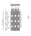
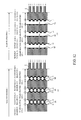
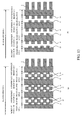
- FIGS. 5 to 7 are views showing a positional relationship between the phase grating GP1 or GP2 of a slab waveguide 1 and an end of an arrayed waveguide 2.
- the respective left sides of FIGS. 5 to 7 show the overall configuration of the optical waveguide.
- the respective right sides of FIGS. 5 and 6 show the self-image SP1 of the phase grating GP1.
- the right side of FIG. 7 shows the self-image SP2 of the phase grating GP2.
- the left and right side drawings are positionally aligned in the vertical direction by an alternative long and short dashed line.
- the positional relationship between the phase grating GP1 of the slab waveguide 1 and the end of the arrayed waveguide 2 is different from each other.
- an incident region IN, a phase grating GP1-1, an interference region IF-1, a phase grating GP1-2, an interference region IF-2, a phase grating GP1-3, and an interference region IF-3 are arranged in this order from the left side to the right side in FIG. 5 .
- the incident region IN, a phase grating GP1-4, an interference region IF-4, a phase grating GP1-5, an interference region IF-5, a phase grating GP1-6, and an interference region IF-6 are arranged in this order from the left side to the right side in FIG. 6 .
- the incident region IN, a phase grating GP2-1, an interference region IF-7, a phase grating GP2-2, an interference region IF-8, a phase grating GP2-3, and an interference region IF-9 are arranged in this order from the left side to the right side in FIG. 7 .
- phase gratings GP1-1, GP1-2, and GP1-3 of FIG. 5 as an integrated phase grating GP1 giving a phase difference of 90° to incident light have a function of forming a self-image.
- the phase gratings GP1-4, GP1-5, and GP1-6 of FIG. 6 as an integrated phase grating GP1 giving a phase difference of 90° to incident light have a function of forming a self-image.
- the phase gratings GP2-1, GP2-2, and GP2-3 of FIG. 7 as an integrated phase grating GP2 giving a phase difference of 180° to incident light have a function of forming a self-image.
- the total width in the direction substantially parallel to the light propagation direction is z for clear formation of the self-image SP1 of the phase grating GP1 in FIG. 1 .
- the total width in the direction substantially parallel to the light propagation direction is z for clear formation of the self-image SP1 of the phase grating GP1 in FIG. 1 .
- the total width in the direction substantially parallel to the light propagation direction is z for clear formation of the self-image SP2 of the phase grating GP2 in FIG. 2 .
- the width in the direction substantially parallel to the light propagation direction is designed, the phase grating and the interference region having the designed width are divided into a plurality of regions in a plane substantially vertical to the light propagation direction, and the divided phase gratings and the divided interference regions are alternately arranged in the direction substantially parallel to the light propagation direction.
- the phase grating GP1 or GP2 is formed of regions shown by diagonal lines and white portions having different refractive indices.
- the refractive index of the region shown by the diagonal lines may be higher or lower than the refractive index of the region shown by the white portion.
- Incident light propagates in the region with a high refractive index at low speed and propagates in the region with a low refractive index at high speed.
- the phase grating GP1 or GP2 changes the speed of light according to the position in the vertical direction of FIGS. 5 to 7 and gives a phase difference to the incident light.
- the interference region IF diffraction light in the phase grating GP1 or GP2 is interfered.
- the arrayed waveguide 2 is connected to the end of the slab waveguide 1 in a constructive interference portion shown by the white portion of the self-image SP1 of the phase grating GP1 or the self-image SP2 of the phase grating GP2. Namely, since diffraction light is concentrically distributed in the constructive interference portion shown by the white portion of the self-image SP1 of the phase grating GP1 or the self-image SP2 of the phase grating GP2, the diffraction light propagates as a propagation mode in the arrayed waveguide 2.
- the diffraction light Since the diffraction light is less distributed in a destructive interference portion shown by the diagonal lines of the self-image SP1 of the phase grating GP1 or the self-image SP2 of the phase grating GP2, the diffraction light does not radiate in the clad layer as a radiation mode.
- a plurality of the arrayed waveguides 2 are connected, only a single waveguide may be connected.
- the constructive interference portion shown by the white portion of the self-image SP1 of the phase grating GP1 is formed at the position corresponding to the region shown by the diagonal lines of the phase grating GP1, and the end of the arrayed waveguide 2 is connected to the constructive interference portion.
- the constructive interference portion shown by the white portion of the self-image SP1 of the phase grating GP1 is formed at the position corresponding to the region shown by the white portion of the phase grating GP1, and the end of the arrayed waveguide 2 is connected to the constructive interference portion.
- the constructive interference portion shown by the white portion of the self-image SP2 of the phase grating GP2 is formed at a position advanced in a direction substantially parallel to the light propagation direction from the regions shown by the diagonal lines and the white portion of the phase grating GP2, and the end of the arrayed waveguide 2 is connected to the constructive interference portion.
- the period of the phase grating GP1 is the same as the period of the arrayed waveguide 2 in FIGS. 5 and 6
- the period of the phase grating GP2 is twice the period of the arrayed waveguide 2 in FIG. 7 .
- the self-images SP1 and SP2 of the phase grating GP1 and GP2 are formed according to the wavelength ⁇ of the incident light and the periods of the phase gratings GP1 and GP2 formed in the slab waveguide 1.
- the end of the arrayed waveguide 2 is disposed at the positions of the constructive interference portion s of the self-image SP1 and SP2 of the phase gratings GP1 and GP2, whereby when light enters from the slab waveguide 1 toward the arrayed waveguide 2, the light is concentrated on the arrayed waveguide 2 and propagates as a propagation mode. Accordingly, when the light enters from the slab waveguide 1 toward the arrayed waveguide 2, the insertion loss can be reduced. Due to reciprocity of light, this also applies to the case where the light enters from the arrayed waveguide 2 toward the slab waveguide 1.
- each end of the branched arrayed waveguides 2 is disposed at the position of the constructive interference portion.
- the phase difference given to the incident light by the phase grating may be 90° or 180° or may be 45° or 135°, and phase differences other than the above phase difference may be used as long as the self-image of the phase grating can be clearly formed by the Talbot effect.
- the first case a case where a plurality of the phase gratings is arranged at a distance from each other in the direction substantially parallel to the light propagation direction
- Comparative examples include a case where a single phase grating having a light propagation direction width equal to the total width in the light propagation direction of a plurality of phase gratings is disposed (hereinafter referred to as “the second case") and a case where the refractive index difference between the region having a high refractive index and the region having a low refractive index of a single phase grating is increased, and a light propagation direction width of the single phase grating is reduced (hereinafter referred to as "the third case”), and the present embodiment and the comparative examples will be compared with each other.
- the second case where the light propagation direction width of a single phase grating is large is not suitable.
- the first case where the light propagation direction width of each phase grating is small is suitable even if the total width in the light propagation direction of the plurality of phase gratings in the first case is equal to the light propagation direction width of a single phase grating in the second case.
- the third case where the light propagation direction width of a single phase grating is small is also suitable.
- the third case where the refractive index difference between the region having a high refractive index and the region having a low refractive index is large is not suitable. Namely, in the first case described in the present embodiment, the light radiation from the region having a low refractive index of the phase grating can be reduced, and, at the same time, the additional process such as additional ultraviolet irradiation can be omitted.
- a method of designing an optical waveguide will be described. First, a method of setting a total light propagation direction width L1 of phase gratings GP1 and GP2 will be described. Next, a method of setting a total light propagation direction width L2 of an interference region IF will be described. Finally, a method of setting a position of an end of an arrayed waveguide 2 will be described.
- the total light propagation direction width L1 of the phase grating GP1 is set so that a phase difference given to light by the phase grating GP1 is preferably 80° to 100°, more preferably 90°.
- the total light propagation direction width L1 of the phase grating GP1 is a total width in the light propagation direction of phase gratings GP1-1, GP1-2, and GP1-3 or a total width in the light propagation direction of phase gratings GP1-4, GP1-5, and GP1-6.
- the total light propagation direction width L1 of the phase grating GP2 is set so that a phase difference given to light by the phase grating GP2 is preferably 170° to 190°, more preferably 180°.
- the total light propagation direction width L1 of the phase grating GP2 is a total width in the light propagation direction of phase gratings GP2-1, GP2-2, and GP2-3.
- Wavelength in vacuum of light is represented by ⁇
- a refractive index of a region having a high refractive index is represented by n
- the refractive index of a region having a low refractive index is represented by n - ⁇ n
- it is preferably set to L1 ⁇ /(4nA) so that the phase difference given to light by the phase grating GP1 is 90°.
- L1 is set to be about 35 ⁇ m so that the phase difference given to light by the phase grating GP1 is 90°.
- L1 ⁇ /(2n ⁇ ) so that the phase difference given to light by the phase grating GP2 is 180°.
- L1 is set to be about 70 ⁇ m so that the phase difference given to light by the phase grating GP2 is 180°.
- the phase gratings GP1-1, GP1-2, and GP1-3 are equally set to L1/3, the light propagation direction widths may not be set equally.
- the light propagation direction widths of the phase gratings GP1-4, GP1-5, and GP1-6 are equally set to L1/3, the light propagation direction widths may not be set equally.
- the light propagation direction widths of the phase gratings GP2-1, GP2-2, and GP2-3 are equally set to L1/3, the light propagation direction widths may not be set equally.
- the phase gratings GP1 and GP2 are divided into three regions. However, the division number of the phase gratings GP1 and GP2 is not limited to only three and is determined by the accuracy of a manufacturing method of an embodiment 3.
- the total light propagation direction width L2 of the interference region IF is set based on the description of FIGS. 1 to 4 .
- the total light propagation direction width L2 of the interference region IF is a total width in the light propagation direction of interference regions IF-1, IF-2, and IF-3, a total width in the light propagation direction of interference regions IF-4, IF-5, and IF-6, or a total width in the light propagation direction of interference regions IF-7, IF-8, and IF-9.
- the wavelength in the interference region IF of light is ⁇ /n.
- L2 md 2 /(2( ⁇ /n)) with respect to the phase grating GP1.
- d 10.0 ⁇ m
- ⁇ 1.55 ⁇ m
- n 1.45
- the light propagation direction widths of the interference regions IF-1, IF-2, and IF-3 are equally set to L2/3, the light propagation direction widths may not be set equally.
- the light propagation direction widths of the interference regions IF-4, IF-5, and IF-6 are equally set to L2/3, the light propagation direction widths may not be set equally.
- the light propagation direction widths of the interference regions IF-7, IF-8, and IF-9 are equally set to L2/3, the light propagation direction widths may not be set equally.
- the interference regions IF are divided into three regions. However, the division number of the interference regions IF is not limited to only three and is determined by the accuracy of the manufacturing method of the embodiment 3.
- a constructive interference portion of the self-image SP of the phase grating GP at the terminal end of the slab waveguide 1 is set as the position of the end of the arrayed waveguide 2 based on the description of FIGS. 1 to 4 . It is preferable that among the ends of the plurality of arrayed waveguides 2, the self-image SP of the phase grating GP is clearly formed at not only the end of the central arrayed waveguide 2 but also the ends of the arrayed waveguides 2 disposed at both edges of a plurality of the arrayed waveguide 2.
- the positional relationship between the phase grating GP of the slab waveguide 1 and the end of the arrayed waveguide 2 is preferably the positional relationship shown in FIG. 8 . Namely, it is preferable that the number of the regions having a high refractive index of the phase grating GP is larger than the number of the arrayed waveguides 2.
- phase gratings GP1 and GP2 may have any shape including a shape to be described in the embodiment 3 as long as it has a function of diffracting light.
- the size of the optical waveguide does not increase, the design does not become difficult.
- the propagation loss between the slab waveguide 1 and the arrayed waveguide 2 is approximately 0.45 dB; however, when this invention is employed in the above designing method, the loss can be reduced to not more than 0.1 dB.
- FIG. 9 is a view showing the calculation results of the Talbot effect of the phase grating GP1.
- the incident light enters as parallel light toward the right direction, and the left end of the phase grating GP1-1 of FIG. 5 or the left end of the phase grating GP1-4 of FIG. 6 is arranged at each left end of FIGS. 9(a), 9(b), and 9(c).
- FIG. 9 (a) shows a case where two phase gratings as an integrated phase grating GP1 have a function of forming a self-image.
- FIG. 9 (b) shows a case where four phase gratings as an integrated phase grating GP1 have a function of forming a self-image.
- FIG. 9 (a) shows a case where two phase gratings as an integrated phase grating GP1 have a function of forming a self-image.
- FIG. 9 (b) shows a case where four phase gratings as an integrated phase grating GP1
- FIGS. 9(a) to 9(c) shows a case where eight phase gratings as an integrated phase grating GP1 have a function of forming a self-image.
- the calculation results of the Talbot effect of the phase grating GP1 are similar to the calculation results of the Talbot effect of the phase grating GP1 in FIG. 3 with the exception of that the incident light is parallel light or diffusion light.
- the Talbot effect does not depend on the division number of the phase grating.
- the phase gratings GP1 and GP2 shown in FIGS. 5 to 7 are provided with refractive index difference regions 11.
- the refractive index difference regions 11 are arranged at a distance from each other in a direction substantially vertical to a light propagation direction and a direction substantially parallel to the light propagation direction and have a refractive index different from the refractive index of a region shown by diagonal lines.
- the refractive index difference region 11 has a rectangular shape, the refractive index difference region 11 may have any shape.
- the refractive index of the refractive index difference region 11 may be larger or smaller than the refractive index of the region shown by diagonal lines.
- a region having a high refractive index and a region having a low refractive index are alternately arranged in the direction substantially vertical to the light propagation direction and the direction substantially parallel to the light propagation direction, whereby the phase gratings GP1 and GP2 can be easily formed.
- the method of manufacturing an optical waveguide shown in FIGS. 5 to 7 includes a method using lithography and etching and a method using ultraviolet irradiation.
- SiO 2 fine particles becoming a lower clad layer and SiO 2 -GeO 2 fine particles becoming a core layer are deposited on an Si substrate by a flame hydrolysis deposition method, and are heated and melted to be transparent.
- an unnecessary portion of the core layer is removed by lithography and etching, and an optical circuit pattern is formed.
- an unnecessary portion of the core layer is removed from a portion becoming the refractive index difference region 11.
- the SiO 2 fine particles becoming an upper clad layer are deposited by the flame hydrolysis deposition method, and are heated and melted to be transparent, whereby when the upper clad layer is formed, the portion becoming the refractive index difference region 11 is filled with a clad material. Since the clad material is filled in the portion becoming the refractive index difference region 11, the refractive index of the refractive index difference region 11 is smaller than the refractive index of the region shown by diagonal lines.
- the refractive index difference region 11 is formed by the formation process of the slab waveguide 1 and the arrayed waveguide 2, after the formation of the slab waveguide 1 and the arrayed waveguide 2, grooving is applied to the portion becoming the refractive index difference region 11, and resin and so on with a refractive index different from the refractive index of the core layer may be filled, or the refractive index difference region 11 may be formed with an air space by only grooving.
- the method using ultraviolet irradiation utilizes the phenomenon that the refractive index is increased by ultraviolet irradiation.
- a mask material is formed on the portion becoming the refractive index difference region 11, and the refractive indices of portions other than the portion becoming the refractive index difference region 11 are changed by ultraviolet irradiation, whereby the refractive index difference region 11 is formed.
- the refractive index of the refractive index difference region 11 is lower than the refractive index of the region shown by diagonal lines.
- a mask material is formed on a portion other than the portion becoming the refractive index difference region 11, and the refractive index of the portion becoming the refractive index difference region 11 is changed by ultraviolet irradiation, whereby the refractive index difference region 11 is formed.
- the refractive index of the refractive index difference region 11 is higher than the refractive index of the region shown by diagonal lines.
- the interference region IF may be provided with any material as long as it has a function of interfering light.
- the interference region IF may be provided with at least one of materials including a core material, a clad material, SiO 2 -GeO 2 irradiated with ultraviolet light, resin, and air.
- the method of manufacturing an optical waveguide shown in FIGS. 10 and 11 is similar to the method of manufacturing an optical waveguide shown in FIGS. 5 to 7 .
- an upper clad material, resin, and so on are filled in the refractive index difference region to form the refractive index difference region
- Each phase grating GP1 shown in FIG. 10(a) is provided with the refractive index difference region 12 and convex regions 13 and 14.
- the refractive index difference region 12 is provided with a region with a large width and a region with a small width in the direction substantially vertical to the light propagation direction and is integrated across the entire phase grating GP1.
- the region with a large width is arranged in the slab waveguide 1 at a distance in the direction substantially vertical to the light propagation direction and has a refractive index different from the refractive index of the region shown by diagonal lines.
- the region with a small width is held between the convex regions 13 and 14, has a refractive index equal to the refractive index of the region with a large width, and connects the regions with a large width adjacent thereto.
- the refractive index of the refractive index difference region 12 may be higher or lower than the refractive index of the portion shown by diagonal lines.
- the region having a high refractive index and the region having a low refractive index are alternately arranged in the direction substantially vertical to the light propagation direction, whereby each phase grating GP1 can be easily formed.
- the convex regions 13 and 14 are arranged in the optical waveguide shown in FIG. 10(a) , only the convex region 13 may be disposed as in the optical waveguide shown in FIG. 10(b) , and only the convex region 14 may be disposed as in the optical waveguide shown in FIG. 11(a) .
- the sum of the light propagation direction widths of the convex regions 13 and 14 of all the phase gratings GP1 is set to L1 shown in FIG. 5 .
- the sum of the light propagation direction widths of the convex regions 13 of all the phase gratings GP1 is set to L1 shown in FIG.
- the sum of the light propagation direction widths of the convex regions 14 of all the phase gratings GP1 is set to L1 shown in FIG. 5 .
- the convex regions 13 and 14 may have any shape.
- a concave region between the convex regions 13 adjacent thereto in the direction substantially vertical to the light propagation direction may have any shape.
- a concave region between the convex regions 14 adjacent thereto in the direction substantially vertical to the light propagation direction may have any shape.
- a boundary surface of the incident region IN or the interference region IF may have any shape.
- a boundary surface region BS may be formed on a boundary surface between the convex region 13 and the refractive index difference region 12, on a boundary surface between the convex region 14 and the refractive index difference region 12, and on a boundary surface between the concave region and the refractive index difference region 12.
- the boundary surface region BS may be formed on a boundary surface between the convex region 14 and the refractive index difference region 12, on a boundary surface between the incident region IN or the interference region IF and the refractive index difference region 12, and on a boundary surface between the concave region and the refractive index difference region 12.
- the refractive index difference region 12 has the same refractive index as the refractive index of the clad material constituting the refractive index difference region 12 or a refractive index between the refractive index of the core material constituting the interference region IF and the refractive index of the clad material constituting the refractive index difference region 12.
- the boundary surface region BS whose surface extends in a direction different from directions substantially parallel and vertical to the light propagation direction is formed on a boundary surface between regions having different refractive indices, whereby light reflection can be suppressed, and it is also possible to prevent light from being reflected toward an input/output waveguide connected to the end of the slab waveguide.
- the boundary surface region BS although one kind of material is used as a material of the boundary surface region BS, a plurality of kinds of materials may be used in combination.
- Each phase grating GP1 shown in FIG. 11(b) is provided with the refractive index difference region 12 and an island-shaped region 15.
- the refractive index difference region 12 is provided with a region having a large width and a region having a small width in the direction substantially vertical to the light propagation direction and is integrated across the entirety of each phase grating GP1.
- the regions with a large width are arranged in the slab waveguide 1 at a distance in the direction substantially vertical to the light propagation direction and have a refractive index different from the refractive index of the region shown by diagonal lines.
- the region with a small width is held between the region shown by diagonal lines and the island-shaped region 15, has a refractive index equal to the refractive index of the region with a large width, and connects the regions with a large width adjacent thereto.
- the refractive index of the refractive index difference region 12 may be higher or lower than the refractive index of the portion shown by diagonal lines.
- the region having a high refractive index and the region having a low refractive index are alternately arranged in the direction substantially vertical to the light propagation direction, whereby each phase grating GP1 can be easily formed.
- the sum of the light propagation direction widths of the island-shaped regions 15 of all the phase gratings GP1 is set to L1 shown in FIG. 5 .
- the island-shaped region 15 may have any shape.
- the boundary surface region BS may be formed on a boundary surface between regions having different refractive indices.
- the convex regions 13 and 14 or the island-shaped region 15 are formed on an extension line of the arrayed waveguide 2
- the convex regions 13 and 14 or the island-shaped region 15 may be formed on an extension line between the arrayed waveguides 2 adjacent to each other in the direction substantially vertical to the light propagation direction.
- the convex regions 13 and 14 or the island-shaped region 15 may be formed on both the extension line of the arrayed waveguide 2 and the extension line between the arrayed waveguides 2 adjacent to each other in the direction substantially vertical to the light propagation direction.
- the convex regions 13 and 14 are formed on the extension line of the arrayed waveguide 2 adjacent to each other in the direction substantially vertical to the light propagation direction, and the island-shaped region 15 is formed on the extension line between the arrayed waveguides 2.
- the convex region 13 is formed on the extension line of the arrayed waveguide 2 adjacent to each other in the direction substantially vertical to the light propagation direction, and the convex region 14 is formed on the extension line between the arrayed waveguides 2.
- an arrayed waveguide grating provided with the optical waveguide described in the embodiments 1 to 3 will be described.
- the arrayed waveguide grating one or more first input/output waveguides, a first slab waveguide, a plurality of arrayed waveguides, a second slab waveguide, and one or more second input/output waveguides are connected in this order.
- the first slab waveguide and the plurality of arrayed waveguides constitute the optical waveguide described in the embodiments 1 to 3, serving as a slab waveguide 1 and an arrayed waveguide 2, respectively.
- an arbitrary wavelength of the wavelengths is selected as ⁇ in FIGS. 1 and 2 .
- the arbitrary wavelength is a center wavelength in the plurality of the wavelengths, for example.
- the grating may be disposed in not only the first slab waveguide but also the second slab waveguide.
- the grating may be disposed in only the first slab waveguide, and the transition region of the Patent Documents 1 to 4 or the slope portion of the Patent Document 5 may be disposed in the second slab waveguide.
- An optical waveguide and an arrayed waveguide grating according to the present invention can be utilized in low loss optical fiber communication utilizing wavelength division multiplexing system.
Landscapes
- Physics & Mathematics (AREA)
- General Physics & Mathematics (AREA)
- Optics & Photonics (AREA)
- Engineering & Computer Science (AREA)
- Microelectronics & Electronic Packaging (AREA)
- Optical Integrated Circuits (AREA)
Applications Claiming Priority (2)
| Application Number | Priority Date | Filing Date | Title |
|---|---|---|---|
| JP2010251219A JP5473868B2 (ja) | 2010-11-09 | 2010-11-09 | 光導波路及びアレイ導波路回折格子 |
| PCT/JP2011/071812 WO2012063562A1 (fr) | 2010-11-09 | 2011-09-26 | Guide d'onde optique et réseau de guide d'onde |
Publications (3)
| Publication Number | Publication Date |
|---|---|
| EP2639609A1 true EP2639609A1 (fr) | 2013-09-18 |
| EP2639609A4 EP2639609A4 (fr) | 2017-11-15 |
| EP2639609B1 EP2639609B1 (fr) | 2019-08-28 |
Family
ID=46050717
Family Applications (1)
| Application Number | Title | Priority Date | Filing Date |
|---|---|---|---|
| EP11840066.2A Active EP2639609B1 (fr) | 2010-11-09 | 2011-09-26 | Guide d'onde optique et réseau de guide d'onde |
Country Status (5)
| Country | Link |
|---|---|
| US (1) | US9020310B2 (fr) |
| EP (1) | EP2639609B1 (fr) |
| JP (1) | JP5473868B2 (fr) |
| CN (1) | CN103221855B (fr) |
| WO (1) | WO2012063562A1 (fr) |
Families Citing this family (5)
| Publication number | Priority date | Publication date | Assignee | Title |
|---|---|---|---|---|
| JP5327897B2 (ja) * | 2010-12-22 | 2013-10-30 | Nttエレクトロニクス株式会社 | 光導波路及びアレイ導波路回折格子 |
| JP6055609B2 (ja) | 2012-04-27 | 2016-12-27 | ヘンケルジャパン株式会社 | 電力機器用ホットメルト接着剤 |
| JP2013231113A (ja) | 2012-04-27 | 2013-11-14 | Henkel Japan Ltd | 接着シート |
| ES2872650B2 (es) * | 2020-04-29 | 2022-03-11 | Univ Malaga | Guia de onda periodica sub-longitud de onda enladrillada, adaptador modal, divisor de potencia y divisor de polarizacion que hacen uso de dicha guia de onda |
| CN115166900B (zh) * | 2022-06-20 | 2024-02-09 | 航天恒星科技有限公司 | 一种光栅天线及其设计方法 |
Family Cites Families (13)
| Publication number | Priority date | Publication date | Assignee | Title |
|---|---|---|---|---|
| US5745618A (en) | 1997-02-04 | 1998-04-28 | Lucent Technologies, Inc. | Optical device having low insertion loss |
| JP2001159718A (ja) | 1998-09-03 | 2001-06-12 | Nippon Telegr & Teleph Corp <Ntt> | アレイ導波路型波長合分波回路 |
| JP3539369B2 (ja) * | 2000-08-23 | 2004-07-07 | 日立電線株式会社 | アレイ導波路型光波長合分波器およびその製造方法 |
| JP3726062B2 (ja) * | 2001-04-25 | 2005-12-14 | 日本発条株式会社 | 光合分波器 |
| US7006729B2 (en) | 2001-12-31 | 2006-02-28 | Wavesplitter Technologies, Inc. | Optical components having reduced insertion loss |
| CA2368945A1 (fr) | 2002-01-21 | 2003-07-21 | Guomin Yu | Dispositif de guide d'ondes optiques a affaiblissement d'insertion peu eleve |
| JP2003329861A (ja) * | 2002-05-17 | 2003-11-19 | Hitachi Cable Ltd | 光導波路、光導波路の製造方法およびアレイ導波路型光波長合分波器 |
| JP2004333523A (ja) * | 2003-04-30 | 2004-11-25 | Hitachi Cable Ltd | 光導波路装置 |
| EP1666937B1 (fr) * | 2003-09-12 | 2015-08-12 | Nippon Telegraph And Telephone Corporation | Multiplexeur/demultiplexeur de longueur d'ondes |
| JP2005326561A (ja) * | 2004-05-13 | 2005-11-24 | Hitachi Cable Ltd | 光波長合分波器 |
| JP2006030687A (ja) * | 2004-07-16 | 2006-02-02 | Nippon Telegr & Teleph Corp <Ntt> | 導波路型光合分波回路 |
| JP4625420B2 (ja) * | 2006-04-04 | 2011-02-02 | 日本電信電話株式会社 | 光回路 |
| US20080292239A1 (en) | 2007-05-25 | 2008-11-27 | Jds Uniphase Corporation | Adiabatic Waveguide Transitions |
-
2010
- 2010-11-09 JP JP2010251219A patent/JP5473868B2/ja active Active
-
2011
- 2011-09-26 EP EP11840066.2A patent/EP2639609B1/fr active Active
- 2011-09-26 WO PCT/JP2011/071812 patent/WO2012063562A1/fr not_active Ceased
- 2011-09-26 CN CN201180053933.1A patent/CN103221855B/zh active Active
- 2011-09-26 US US13/881,135 patent/US9020310B2/en active Active
Non-Patent Citations (1)
| Title |
|---|
| See references of WO2012063562A1 * |
Also Published As
| Publication number | Publication date |
|---|---|
| EP2639609A4 (fr) | 2017-11-15 |
| EP2639609B1 (fr) | 2019-08-28 |
| US9020310B2 (en) | 2015-04-28 |
| JP2012103435A (ja) | 2012-05-31 |
| US20130209036A1 (en) | 2013-08-15 |
| WO2012063562A1 (fr) | 2012-05-18 |
| CN103221855B (zh) | 2015-07-22 |
| CN103221855A (zh) | 2013-07-24 |
| JP5473868B2 (ja) | 2014-04-16 |
Similar Documents
| Publication | Publication Date | Title |
|---|---|---|
| US20080292239A1 (en) | Adiabatic Waveguide Transitions | |
| US6304706B1 (en) | Planar lightwave circuit | |
| EP2639609A1 (fr) | Guide d'onde optique et réseau de guide d'onde | |
| US12541145B2 (en) | Photomask, optical-waveguide, optical circuit and method of manufacturing an optical-waveguide | |
| EP2657735B1 (fr) | Guide d'ondes optique et réseau de diffraction à guides d'ondes optiques groupés | |
| EP1251652A2 (fr) | Multiplexeur/démultiplexeur optique à réseau de guides d'ondes | |
| US20030206694A1 (en) | Photonic multi-bandgap lightwave device and methods for manufacturing thereof | |
| US10054738B2 (en) | Optical waveguide and arrayed waveguide grating | |
| US6798952B2 (en) | Optical multiplexer/demultiplexer | |
| JP7185165B2 (ja) | 光導波路チップ | |
| JP2013041146A (ja) | 波長選択性多モード干渉導波路デバイス | |
| EP2518547B1 (fr) | Circuit optique planaire et procédé de fabrication de celui-ci | |
| JP2000235123A (ja) | 光波長合分波器 | |
| JP4091944B2 (ja) | 光回路 | |
| JP2007093721A (ja) | 光波長合分波器 | |
| EP1405115A2 (fr) | Aplatissement de la bande passante dans un reseau a guide d'onde en faisceau | |
| JP2005099782A (ja) | 光機能回路 | |
| JPH04326307A (ja) | 集積化光合分波器 |
Legal Events
| Date | Code | Title | Description |
|---|---|---|---|
| PUAI | Public reference made under article 153(3) epc to a published international application that has entered the european phase |
Free format text: ORIGINAL CODE: 0009012 |
|
| 17P | Request for examination filed |
Effective date: 20130610 |
|
| AK | Designated contracting states |
Kind code of ref document: A1 Designated state(s): AL AT BE BG CH CY CZ DE DK EE ES FI FR GB GR HR HU IE IS IT LI LT LU LV MC MK MT NL NO PL PT RO RS SE SI SK SM TR |
|
| DAX | Request for extension of the european patent (deleted) | ||
| RA4 | Supplementary search report drawn up and despatched (corrected) |
Effective date: 20171018 |
|
| RIC1 | Information provided on ipc code assigned before grant |
Ipc: G02B 6/12 20060101ALI20171012BHEP Ipc: G02B 6/122 20060101AFI20171012BHEP |
|
| GRAP | Despatch of communication of intention to grant a patent |
Free format text: ORIGINAL CODE: EPIDOSNIGR1 |
|
| STAA | Information on the status of an ep patent application or granted ep patent |
Free format text: STATUS: GRANT OF PATENT IS INTENDED |
|
| INTG | Intention to grant announced |
Effective date: 20180926 |
|
| GRAS | Grant fee paid |
Free format text: ORIGINAL CODE: EPIDOSNIGR3 |
|
| GRAJ | Information related to disapproval of communication of intention to grant by the applicant or resumption of examination proceedings by the epo deleted |
Free format text: ORIGINAL CODE: EPIDOSDIGR1 |
|
| GRAL | Information related to payment of fee for publishing/printing deleted |
Free format text: ORIGINAL CODE: EPIDOSDIGR3 |
|
| STAA | Information on the status of an ep patent application or granted ep patent |
Free format text: STATUS: REQUEST FOR EXAMINATION WAS MADE |
|
| INTC | Intention to grant announced (deleted) | ||
| GRAP | Despatch of communication of intention to grant a patent |
Free format text: ORIGINAL CODE: EPIDOSNIGR1 |
|
| STAA | Information on the status of an ep patent application or granted ep patent |
Free format text: STATUS: GRANT OF PATENT IS INTENDED |
|
| INTG | Intention to grant announced |
Effective date: 20190328 |
|
| GRAA | (expected) grant |
Free format text: ORIGINAL CODE: 0009210 |
|
| STAA | Information on the status of an ep patent application or granted ep patent |
Free format text: STATUS: THE PATENT HAS BEEN GRANTED |
|
| AK | Designated contracting states |
Kind code of ref document: B1 Designated state(s): AL AT BE BG CH CY CZ DE DK EE ES FI FR GB GR HR HU IE IS IT LI LT LU LV MC MK MT NL NO PL PT RO RS SE SI SK SM TR |
|
| REG | Reference to a national code |
Ref country code: GB Ref legal event code: FG4D |
|
| REG | Reference to a national code |
Ref country code: CH Ref legal event code: EP |
|
| REG | Reference to a national code |
Ref country code: AT Ref legal event code: REF Ref document number: 1173109 Country of ref document: AT Kind code of ref document: T Effective date: 20190915 |
|
| REG | Reference to a national code |
Ref country code: IE Ref legal event code: FG4D |
|
| REG | Reference to a national code |
Ref country code: DE Ref legal event code: R096 Ref document number: 602011061683 Country of ref document: DE |
|
| REG | Reference to a national code |
Ref country code: NL Ref legal event code: MP Effective date: 20190828 |
|
| REG | Reference to a national code |
Ref country code: LT Ref legal event code: MG4D |
|
| PG25 | Lapsed in a contracting state [announced via postgrant information from national office to epo] |
Ref country code: NO Free format text: LAPSE BECAUSE OF FAILURE TO SUBMIT A TRANSLATION OF THE DESCRIPTION OR TO PAY THE FEE WITHIN THE PRESCRIBED TIME-LIMIT Effective date: 20191128 Ref country code: FI Free format text: LAPSE BECAUSE OF FAILURE TO SUBMIT A TRANSLATION OF THE DESCRIPTION OR TO PAY THE FEE WITHIN THE PRESCRIBED TIME-LIMIT Effective date: 20190828 Ref country code: PT Free format text: LAPSE BECAUSE OF FAILURE TO SUBMIT A TRANSLATION OF THE DESCRIPTION OR TO PAY THE FEE WITHIN THE PRESCRIBED TIME-LIMIT Effective date: 20191230 Ref country code: LT Free format text: LAPSE BECAUSE OF FAILURE TO SUBMIT A TRANSLATION OF THE DESCRIPTION OR TO PAY THE FEE WITHIN THE PRESCRIBED TIME-LIMIT Effective date: 20190828 Ref country code: HR Free format text: LAPSE BECAUSE OF FAILURE TO SUBMIT A TRANSLATION OF THE DESCRIPTION OR TO PAY THE FEE WITHIN THE PRESCRIBED TIME-LIMIT Effective date: 20190828 Ref country code: NL Free format text: LAPSE BECAUSE OF FAILURE TO SUBMIT A TRANSLATION OF THE DESCRIPTION OR TO PAY THE FEE WITHIN THE PRESCRIBED TIME-LIMIT Effective date: 20190828 Ref country code: BG Free format text: LAPSE BECAUSE OF FAILURE TO SUBMIT A TRANSLATION OF THE DESCRIPTION OR TO PAY THE FEE WITHIN THE PRESCRIBED TIME-LIMIT Effective date: 20191128 Ref country code: SE Free format text: LAPSE BECAUSE OF FAILURE TO SUBMIT A TRANSLATION OF THE DESCRIPTION OR TO PAY THE FEE WITHIN THE PRESCRIBED TIME-LIMIT Effective date: 20190828 |
|
| PG25 | Lapsed in a contracting state [announced via postgrant information from national office to epo] |
Ref country code: GR Free format text: LAPSE BECAUSE OF FAILURE TO SUBMIT A TRANSLATION OF THE DESCRIPTION OR TO PAY THE FEE WITHIN THE PRESCRIBED TIME-LIMIT Effective date: 20191129 Ref country code: LV Free format text: LAPSE BECAUSE OF FAILURE TO SUBMIT A TRANSLATION OF THE DESCRIPTION OR TO PAY THE FEE WITHIN THE PRESCRIBED TIME-LIMIT Effective date: 20190828 Ref country code: AL Free format text: LAPSE BECAUSE OF FAILURE TO SUBMIT A TRANSLATION OF THE DESCRIPTION OR TO PAY THE FEE WITHIN THE PRESCRIBED TIME-LIMIT Effective date: 20190828 Ref country code: RS Free format text: LAPSE BECAUSE OF FAILURE TO SUBMIT A TRANSLATION OF THE DESCRIPTION OR TO PAY THE FEE WITHIN THE PRESCRIBED TIME-LIMIT Effective date: 20190828 Ref country code: IS Free format text: LAPSE BECAUSE OF FAILURE TO SUBMIT A TRANSLATION OF THE DESCRIPTION OR TO PAY THE FEE WITHIN THE PRESCRIBED TIME-LIMIT Effective date: 20191228 Ref country code: ES Free format text: LAPSE BECAUSE OF FAILURE TO SUBMIT A TRANSLATION OF THE DESCRIPTION OR TO PAY THE FEE WITHIN THE PRESCRIBED TIME-LIMIT Effective date: 20190828 |
|
| REG | Reference to a national code |
Ref country code: AT Ref legal event code: MK05 Ref document number: 1173109 Country of ref document: AT Kind code of ref document: T Effective date: 20190828 |
|
| PG25 | Lapsed in a contracting state [announced via postgrant information from national office to epo] |
Ref country code: TR Free format text: LAPSE BECAUSE OF FAILURE TO SUBMIT A TRANSLATION OF THE DESCRIPTION OR TO PAY THE FEE WITHIN THE PRESCRIBED TIME-LIMIT Effective date: 20190828 |
|
| PG25 | Lapsed in a contracting state [announced via postgrant information from national office to epo] |
Ref country code: RO Free format text: LAPSE BECAUSE OF FAILURE TO SUBMIT A TRANSLATION OF THE DESCRIPTION OR TO PAY THE FEE WITHIN THE PRESCRIBED TIME-LIMIT Effective date: 20190828 Ref country code: IT Free format text: LAPSE BECAUSE OF FAILURE TO SUBMIT A TRANSLATION OF THE DESCRIPTION OR TO PAY THE FEE WITHIN THE PRESCRIBED TIME-LIMIT Effective date: 20190828 Ref country code: PL Free format text: LAPSE BECAUSE OF FAILURE TO SUBMIT A TRANSLATION OF THE DESCRIPTION OR TO PAY THE FEE WITHIN THE PRESCRIBED TIME-LIMIT Effective date: 20190828 Ref country code: DK Free format text: LAPSE BECAUSE OF FAILURE TO SUBMIT A TRANSLATION OF THE DESCRIPTION OR TO PAY THE FEE WITHIN THE PRESCRIBED TIME-LIMIT Effective date: 20190828 Ref country code: AT Free format text: LAPSE BECAUSE OF FAILURE TO SUBMIT A TRANSLATION OF THE DESCRIPTION OR TO PAY THE FEE WITHIN THE PRESCRIBED TIME-LIMIT Effective date: 20190828 Ref country code: EE Free format text: LAPSE BECAUSE OF FAILURE TO SUBMIT A TRANSLATION OF THE DESCRIPTION OR TO PAY THE FEE WITHIN THE PRESCRIBED TIME-LIMIT Effective date: 20190828 |
|
| PG25 | Lapsed in a contracting state [announced via postgrant information from national office to epo] |
Ref country code: CZ Free format text: LAPSE BECAUSE OF FAILURE TO SUBMIT A TRANSLATION OF THE DESCRIPTION OR TO PAY THE FEE WITHIN THE PRESCRIBED TIME-LIMIT Effective date: 20190828 Ref country code: SM Free format text: LAPSE BECAUSE OF FAILURE TO SUBMIT A TRANSLATION OF THE DESCRIPTION OR TO PAY THE FEE WITHIN THE PRESCRIBED TIME-LIMIT Effective date: 20190828 Ref country code: SK Free format text: LAPSE BECAUSE OF FAILURE TO SUBMIT A TRANSLATION OF THE DESCRIPTION OR TO PAY THE FEE WITHIN THE PRESCRIBED TIME-LIMIT Effective date: 20190828 Ref country code: MC Free format text: LAPSE BECAUSE OF FAILURE TO SUBMIT A TRANSLATION OF THE DESCRIPTION OR TO PAY THE FEE WITHIN THE PRESCRIBED TIME-LIMIT Effective date: 20190828 Ref country code: IS Free format text: LAPSE BECAUSE OF FAILURE TO SUBMIT A TRANSLATION OF THE DESCRIPTION OR TO PAY THE FEE WITHIN THE PRESCRIBED TIME-LIMIT Effective date: 20200224 |
|
| REG | Reference to a national code |
Ref country code: CH Ref legal event code: PL |
|
| REG | Reference to a national code |
Ref country code: DE Ref legal event code: R097 Ref document number: 602011061683 Country of ref document: DE |
|
| PLBE | No opposition filed within time limit |
Free format text: ORIGINAL CODE: 0009261 |
|
| STAA | Information on the status of an ep patent application or granted ep patent |
Free format text: STATUS: NO OPPOSITION FILED WITHIN TIME LIMIT |
|
| PG2D | Information on lapse in contracting state deleted |
Ref country code: IS |
|
| PG25 | Lapsed in a contracting state [announced via postgrant information from national office to epo] |
Ref country code: LI Free format text: LAPSE BECAUSE OF NON-PAYMENT OF DUE FEES Effective date: 20190930 Ref country code: CH Free format text: LAPSE BECAUSE OF NON-PAYMENT OF DUE FEES Effective date: 20190930 Ref country code: IE Free format text: LAPSE BECAUSE OF NON-PAYMENT OF DUE FEES Effective date: 20190926 Ref country code: LU Free format text: LAPSE BECAUSE OF NON-PAYMENT OF DUE FEES Effective date: 20190926 |
|
| REG | Reference to a national code |
Ref country code: BE Ref legal event code: MM Effective date: 20190930 |
|
| 26N | No opposition filed |
Effective date: 20200603 |
|
| PG25 | Lapsed in a contracting state [announced via postgrant information from national office to epo] |
Ref country code: BE Free format text: LAPSE BECAUSE OF NON-PAYMENT OF DUE FEES Effective date: 20190930 Ref country code: SI Free format text: LAPSE BECAUSE OF FAILURE TO SUBMIT A TRANSLATION OF THE DESCRIPTION OR TO PAY THE FEE WITHIN THE PRESCRIBED TIME-LIMIT Effective date: 20190828 |
|
| GBPC | Gb: european patent ceased through non-payment of renewal fee |
Effective date: 20191128 |
|
| PG25 | Lapsed in a contracting state [announced via postgrant information from national office to epo] |
Ref country code: GB Free format text: LAPSE BECAUSE OF NON-PAYMENT OF DUE FEES Effective date: 20191128 |
|
| PG25 | Lapsed in a contracting state [announced via postgrant information from national office to epo] |
Ref country code: CY Free format text: LAPSE BECAUSE OF FAILURE TO SUBMIT A TRANSLATION OF THE DESCRIPTION OR TO PAY THE FEE WITHIN THE PRESCRIBED TIME-LIMIT Effective date: 20190828 |
|
| PG25 | Lapsed in a contracting state [announced via postgrant information from national office to epo] |
Ref country code: MT Free format text: LAPSE BECAUSE OF FAILURE TO SUBMIT A TRANSLATION OF THE DESCRIPTION OR TO PAY THE FEE WITHIN THE PRESCRIBED TIME-LIMIT Effective date: 20190828 Ref country code: HU Free format text: LAPSE BECAUSE OF FAILURE TO SUBMIT A TRANSLATION OF THE DESCRIPTION OR TO PAY THE FEE WITHIN THE PRESCRIBED TIME-LIMIT; INVALID AB INITIO Effective date: 20110926 |
|
| PG25 | Lapsed in a contracting state [announced via postgrant information from national office to epo] |
Ref country code: MK Free format text: LAPSE BECAUSE OF FAILURE TO SUBMIT A TRANSLATION OF THE DESCRIPTION OR TO PAY THE FEE WITHIN THE PRESCRIBED TIME-LIMIT Effective date: 20190828 |
|
| PGFP | Annual fee paid to national office [announced via postgrant information from national office to epo] |
Ref country code: DE Payment date: 20250730 Year of fee payment: 15 |
|
| PGFP | Annual fee paid to national office [announced via postgrant information from national office to epo] |
Ref country code: FR Payment date: 20250808 Year of fee payment: 15 |