EP2641996A1 - Procédé de croissance de cristaux à base de magnésium-zinc-oxyde - Google Patents
Procédé de croissance de cristaux à base de magnésium-zinc-oxyde Download PDFInfo
- Publication number
- EP2641996A1 EP2641996A1 EP13001444.2A EP13001444A EP2641996A1 EP 2641996 A1 EP2641996 A1 EP 2641996A1 EP 13001444 A EP13001444 A EP 13001444A EP 2641996 A1 EP2641996 A1 EP 2641996A1
- Authority
- EP
- European Patent Office
- Prior art keywords
- growth
- crystal
- mgzno
- crystal layer
- zno
- Prior art date
- Legal status (The legal status is an assumption and is not a legal conclusion. Google has not performed a legal analysis and makes no representation as to the accuracy of the status listed.)
- Withdrawn
Links
Images









Classifications
-
- C—CHEMISTRY; METALLURGY
- C30—CRYSTAL GROWTH
- C30B—SINGLE-CRYSTAL GROWTH; UNIDIRECTIONAL SOLIDIFICATION OF EUTECTIC MATERIAL OR UNIDIRECTIONAL DEMIXING OF EUTECTOID MATERIAL; REFINING BY ZONE-MELTING OF MATERIAL; PRODUCTION OF A HOMOGENEOUS POLYCRYSTALLINE MATERIAL WITH DEFINED STRUCTURE; SINGLE CRYSTALS OR HOMOGENEOUS POLYCRYSTALLINE MATERIAL WITH DEFINED STRUCTURE; AFTER-TREATMENT OF SINGLE CRYSTALS OR A HOMOGENEOUS POLYCRYSTALLINE MATERIAL WITH DEFINED STRUCTURE; APPARATUS THEREFOR
- C30B25/00—Single-crystal growth by chemical reaction of reactive gases, e.g. chemical vapour-deposition growth
- C30B25/02—Epitaxial-layer growth
- C30B25/18—Epitaxial-layer growth characterised by the substrate
-
- C—CHEMISTRY; METALLURGY
- C23—COATING METALLIC MATERIAL; COATING MATERIAL WITH METALLIC MATERIAL; CHEMICAL SURFACE TREATMENT; DIFFUSION TREATMENT OF METALLIC MATERIAL; COATING BY VACUUM EVAPORATION, BY SPUTTERING, BY ION IMPLANTATION OR BY CHEMICAL VAPOUR DEPOSITION, IN GENERAL; INHIBITING CORROSION OF METALLIC MATERIAL OR INCRUSTATION IN GENERAL
- C23C—COATING METALLIC MATERIAL; COATING MATERIAL WITH METALLIC MATERIAL; SURFACE TREATMENT OF METALLIC MATERIAL BY DIFFUSION INTO THE SURFACE, BY CHEMICAL CONVERSION OR SUBSTITUTION; COATING BY VACUUM EVAPORATION, BY SPUTTERING, BY ION IMPLANTATION OR BY CHEMICAL VAPOUR DEPOSITION, IN GENERAL
- C23C16/00—Chemical coating by decomposition of gaseous compounds, without leaving reaction products of surface material in the coating, i.e. chemical vapour deposition [CVD] processes
- C23C16/22—Chemical coating by decomposition of gaseous compounds, without leaving reaction products of surface material in the coating, i.e. chemical vapour deposition [CVD] processes characterised by the deposition of inorganic material, other than metallic material
- C23C16/30—Deposition of compounds, mixtures or solid solutions, e.g. borides, carbides, nitrides
- C23C16/40—Oxides
- C23C16/403—Oxides of aluminium, magnesium or beryllium
-
- C—CHEMISTRY; METALLURGY
- C23—COATING METALLIC MATERIAL; COATING MATERIAL WITH METALLIC MATERIAL; CHEMICAL SURFACE TREATMENT; DIFFUSION TREATMENT OF METALLIC MATERIAL; COATING BY VACUUM EVAPORATION, BY SPUTTERING, BY ION IMPLANTATION OR BY CHEMICAL VAPOUR DEPOSITION, IN GENERAL; INHIBITING CORROSION OF METALLIC MATERIAL OR INCRUSTATION IN GENERAL
- C23C—COATING METALLIC MATERIAL; COATING MATERIAL WITH METALLIC MATERIAL; SURFACE TREATMENT OF METALLIC MATERIAL BY DIFFUSION INTO THE SURFACE, BY CHEMICAL CONVERSION OR SUBSTITUTION; COATING BY VACUUM EVAPORATION, BY SPUTTERING, BY ION IMPLANTATION OR BY CHEMICAL VAPOUR DEPOSITION, IN GENERAL
- C23C16/00—Chemical coating by decomposition of gaseous compounds, without leaving reaction products of surface material in the coating, i.e. chemical vapour deposition [CVD] processes
- C23C16/22—Chemical coating by decomposition of gaseous compounds, without leaving reaction products of surface material in the coating, i.e. chemical vapour deposition [CVD] processes characterised by the deposition of inorganic material, other than metallic material
- C23C16/30—Deposition of compounds, mixtures or solid solutions, e.g. borides, carbides, nitrides
- C23C16/40—Oxides
- C23C16/407—Oxides of zinc, germanium, cadmium, indium, tin, thallium or bismuth
-
- C—CHEMISTRY; METALLURGY
- C23—COATING METALLIC MATERIAL; COATING MATERIAL WITH METALLIC MATERIAL; CHEMICAL SURFACE TREATMENT; DIFFUSION TREATMENT OF METALLIC MATERIAL; COATING BY VACUUM EVAPORATION, BY SPUTTERING, BY ION IMPLANTATION OR BY CHEMICAL VAPOUR DEPOSITION, IN GENERAL; INHIBITING CORROSION OF METALLIC MATERIAL OR INCRUSTATION IN GENERAL
- C23C—COATING METALLIC MATERIAL; COATING MATERIAL WITH METALLIC MATERIAL; SURFACE TREATMENT OF METALLIC MATERIAL BY DIFFUSION INTO THE SURFACE, BY CHEMICAL CONVERSION OR SUBSTITUTION; COATING BY VACUUM EVAPORATION, BY SPUTTERING, BY ION IMPLANTATION OR BY CHEMICAL VAPOUR DEPOSITION, IN GENERAL
- C23C16/00—Chemical coating by decomposition of gaseous compounds, without leaving reaction products of surface material in the coating, i.e. chemical vapour deposition [CVD] processes
- C23C16/44—Chemical coating by decomposition of gaseous compounds, without leaving reaction products of surface material in the coating, i.e. chemical vapour deposition [CVD] processes characterised by the method of coating
- C23C16/455—Chemical coating by decomposition of gaseous compounds, without leaving reaction products of surface material in the coating, i.e. chemical vapour deposition [CVD] processes characterised by the method of coating characterised by the method used for introducing gases into reaction chamber or for modifying gas flows in reaction chamber
- C23C16/45561—Gas plumbing upstream of the reaction chamber
-
- C—CHEMISTRY; METALLURGY
- C30—CRYSTAL GROWTH
- C30B—SINGLE-CRYSTAL GROWTH; UNIDIRECTIONAL SOLIDIFICATION OF EUTECTIC MATERIAL OR UNIDIRECTIONAL DEMIXING OF EUTECTOID MATERIAL; REFINING BY ZONE-MELTING OF MATERIAL; PRODUCTION OF A HOMOGENEOUS POLYCRYSTALLINE MATERIAL WITH DEFINED STRUCTURE; SINGLE CRYSTALS OR HOMOGENEOUS POLYCRYSTALLINE MATERIAL WITH DEFINED STRUCTURE; AFTER-TREATMENT OF SINGLE CRYSTALS OR A HOMOGENEOUS POLYCRYSTALLINE MATERIAL WITH DEFINED STRUCTURE; APPARATUS THEREFOR
- C30B25/00—Single-crystal growth by chemical reaction of reactive gases, e.g. chemical vapour-deposition growth
- C30B25/02—Epitaxial-layer growth
- C30B25/18—Epitaxial-layer growth characterised by the substrate
- C30B25/183—Epitaxial-layer growth characterised by the substrate being provided with a buffer layer, e.g. a lattice matching layer
-
- C—CHEMISTRY; METALLURGY
- C30—CRYSTAL GROWTH
- C30B—SINGLE-CRYSTAL GROWTH; UNIDIRECTIONAL SOLIDIFICATION OF EUTECTIC MATERIAL OR UNIDIRECTIONAL DEMIXING OF EUTECTOID MATERIAL; REFINING BY ZONE-MELTING OF MATERIAL; PRODUCTION OF A HOMOGENEOUS POLYCRYSTALLINE MATERIAL WITH DEFINED STRUCTURE; SINGLE CRYSTALS OR HOMOGENEOUS POLYCRYSTALLINE MATERIAL WITH DEFINED STRUCTURE; AFTER-TREATMENT OF SINGLE CRYSTALS OR A HOMOGENEOUS POLYCRYSTALLINE MATERIAL WITH DEFINED STRUCTURE; APPARATUS THEREFOR
- C30B25/00—Single-crystal growth by chemical reaction of reactive gases, e.g. chemical vapour-deposition growth
- C30B25/02—Epitaxial-layer growth
- C30B25/18—Epitaxial-layer growth characterised by the substrate
- C30B25/20—Epitaxial-layer growth characterised by the substrate the substrate being of the same materials as the epitaxial layer
- C30B25/205—Epitaxial-layer growth characterised by the substrate the substrate being of the same materials as the epitaxial layer the substrate being of insulating material
-
- C—CHEMISTRY; METALLURGY
- C30—CRYSTAL GROWTH
- C30B—SINGLE-CRYSTAL GROWTH; UNIDIRECTIONAL SOLIDIFICATION OF EUTECTIC MATERIAL OR UNIDIRECTIONAL DEMIXING OF EUTECTOID MATERIAL; REFINING BY ZONE-MELTING OF MATERIAL; PRODUCTION OF A HOMOGENEOUS POLYCRYSTALLINE MATERIAL WITH DEFINED STRUCTURE; SINGLE CRYSTALS OR HOMOGENEOUS POLYCRYSTALLINE MATERIAL WITH DEFINED STRUCTURE; AFTER-TREATMENT OF SINGLE CRYSTALS OR A HOMOGENEOUS POLYCRYSTALLINE MATERIAL WITH DEFINED STRUCTURE; APPARATUS THEREFOR
- C30B29/00—Single crystals or homogeneous polycrystalline material with defined structure characterised by the material or by their shape
- C30B29/10—Inorganic compounds or compositions
- C30B29/16—Oxides
-
- H—ELECTRICITY
- H10—SEMICONDUCTOR DEVICES; ELECTRIC SOLID-STATE DEVICES NOT OTHERWISE PROVIDED FOR
- H10P—GENERIC PROCESSES OR APPARATUS FOR THE MANUFACTURE OR TREATMENT OF DEVICES COVERED BY CLASS H10
- H10P14/00—Formation of materials, e.g. in the shape of layers or pillars
- H10P14/20—Formation of materials, e.g. in the shape of layers or pillars of semiconductor materials
- H10P14/24—Formation of materials, e.g. in the shape of layers or pillars of semiconductor materials using chemical vapour deposition [CVD]
-
- H—ELECTRICITY
- H10—SEMICONDUCTOR DEVICES; ELECTRIC SOLID-STATE DEVICES NOT OTHERWISE PROVIDED FOR
- H10P—GENERIC PROCESSES OR APPARATUS FOR THE MANUFACTURE OR TREATMENT OF DEVICES COVERED BY CLASS H10
- H10P14/00—Formation of materials, e.g. in the shape of layers or pillars
- H10P14/20—Formation of materials, e.g. in the shape of layers or pillars of semiconductor materials
- H10P14/34—Deposited materials, e.g. layers
- H10P14/3402—Deposited materials, e.g. layers characterised by the chemical composition
- H10P14/3424—Deposited materials, e.g. layers characterised by the chemical composition being Group IIB-VIA materials
- H10P14/3426—Oxides
-
- H—ELECTRICITY
- H10—SEMICONDUCTOR DEVICES; ELECTRIC SOLID-STATE DEVICES NOT OTHERWISE PROVIDED FOR
- H10P—GENERIC PROCESSES OR APPARATUS FOR THE MANUFACTURE OR TREATMENT OF DEVICES COVERED BY CLASS H10
- H10P14/00—Formation of materials, e.g. in the shape of layers or pillars
- H10P14/20—Formation of materials, e.g. in the shape of layers or pillars of semiconductor materials
- H10P14/34—Deposited materials, e.g. layers
- H10P14/3402—Deposited materials, e.g. layers characterised by the chemical composition
- H10P14/3434—Deposited materials, e.g. layers characterised by the chemical composition being oxide semiconductor materials
-
- H—ELECTRICITY
- H10—SEMICONDUCTOR DEVICES; ELECTRIC SOLID-STATE DEVICES NOT OTHERWISE PROVIDED FOR
- H10P—GENERIC PROCESSES OR APPARATUS FOR THE MANUFACTURE OR TREATMENT OF DEVICES COVERED BY CLASS H10
- H10P14/00—Formation of materials, e.g. in the shape of layers or pillars
- H10P14/20—Formation of materials, e.g. in the shape of layers or pillars of semiconductor materials
- H10P14/34—Deposited materials, e.g. layers
- H10P14/3438—Doping during depositing
- H10P14/3441—Conductivity type
- H10P14/3442—N-type
-
- C—CHEMISTRY; METALLURGY
- C30—CRYSTAL GROWTH
- C30B—SINGLE-CRYSTAL GROWTH; UNIDIRECTIONAL SOLIDIFICATION OF EUTECTIC MATERIAL OR UNIDIRECTIONAL DEMIXING OF EUTECTOID MATERIAL; REFINING BY ZONE-MELTING OF MATERIAL; PRODUCTION OF A HOMOGENEOUS POLYCRYSTALLINE MATERIAL WITH DEFINED STRUCTURE; SINGLE CRYSTALS OR HOMOGENEOUS POLYCRYSTALLINE MATERIAL WITH DEFINED STRUCTURE; AFTER-TREATMENT OF SINGLE CRYSTALS OR A HOMOGENEOUS POLYCRYSTALLINE MATERIAL WITH DEFINED STRUCTURE; APPARATUS THEREFOR
- C30B25/00—Single-crystal growth by chemical reaction of reactive gases, e.g. chemical vapour-deposition growth
- C30B25/02—Epitaxial-layer growth
- C30B25/18—Epitaxial-layer growth characterised by the substrate
- C30B25/186—Epitaxial-layer growth characterised by the substrate being specially pre-treated by, e.g. chemical or physical means
Definitions
- the present invention relates to a method for growing a magnesium-zinc-oxide (MgZnO) based crystal, and in particular, to a method for growing a MgZnO-based crystal by MOCVD.
- MgZnO magnesium-zinc-oxide
- Zinc oxide is a direct-transition-type semiconductor having a bandgap energy of 3.37 eV at room temperature, and holds promise as a material for an optical element in the blue to purple regions.
- zinc oxide has characteristics that are extremely suited to a semiconductor light-emitting element. It is suitable not only for light-emitting elements and light-receiving elements but also for a broad range of applications such as surface acoustic wave (SAW) devices and piezoelectric elements. Moreover, it has characteristics of being made from inexpensive raw materials and being harmless to the environment or the human body.
- SAW surface acoustic wave
- MOCVD metal organic chemical vapor deposition
- MBE molecular beam epitaxy
- PLD pulsed laser deposition
- MOCVD has advantages in that the equipment is relatively inexpensive, crystal growth can be performed over a large area, a plurality of crystals can be grown simultaneously, the throughput is high, and the method is excellent in terms of mass productivity and cost.
- a semiconductor light-emitting element such as a light-emitting diode (LED)
- LED light-emitting diode
- the light-emitting layer is a ZnO crystal layer
- MgZnO crystal layers are used for the p-type semiconductor layer and the n-type semiconductor layer.
- the band gap can be increased while a Wurtzite structure as with a ZnO crystal is maintained if the Mg composition (x) is no more than 0.68.
- Patent Document 1 Japanese Unexamined Patent Application Publication, JP-A 2010-272807 .
- Patent Document 2 JP-A 2006-73726 discloses a method in which amorphous MgZnO film-formed at a low temperature is heat-treated and crystallized, and a MgZnO crystal is subsequently film-formed at a high temperature.
- Patent Document 3 JP-A 2008-244011 )discloses a method for film-forming a ZnO crystal in which steps of growing a ZnO thin film at a low temperature and performing heat treatment at a high temperature in a reductive atmosphere are repeated.
- Patent Document 4 JP-A 2008-243987
- Patent Document 5 JP-A 2010-10629 disclose difficulties in growing ZnO-based crystal grown using MOCVD.
- a semiconductor element such as a light-emitting diode (LED)
- LED light-emitting diode
- Particularly important for obtaining p-type and n-type MgZnO crystal layers is establishment of a technique for growing an MgZnO crystal having a low residual carrier concentration.
- a ZnO crystal has a hexagonal Wurtzite structure, and an MgO crystal has a cubic rock salt structure.
- An Mg x Zn 1-x O crystal which is a mixed crystal of the two above crystals, has a Wurtzite structure when the Mg composition (x) is between 0 and 0.68. If an MgZnO crystal is grown on a c-plane ZnO crystal, the a-axis length of the MgZnO crystal matches the a-axis length of the ZnO crystal; therefore, the a-axis length decreases and the c-axis length increases. In other words, the MgZnO crystal layer is a crystal that contains a strain.
- P-type and n-type semiconductor layers are formed by supplying a material gas containing an impurity element during crystal growth.
- the material gas containing an impurity element is subjected to a thermal decomposition reaction and then incorporated into the Mg x Zn 1-x O crystal layer, as with the zinc-based organometalic material gas, magnesium-based organometalic material gas, and water vapor.
- the impurity element replaces the Zn site, the Mg site or the O (oxygen) site.
- the impurity element readily forms, with oxygen, oxide crystals having a variety of crystal structures, and may disrupt the crystal structure of the Mg x Zn 1-x O crystal layer.
- the impurity element therefore causes problems similar to those described above in (i)-(iii). Also, it is important, when the carrier concentration in the semiconductor layer is adjusted, that the residual carrier concentration in the semiconductor layer is sufficiently lower than the carrier concentration to be adjusted.
- the present invention was conceived in light of the abovementioned problems, it being an object thereof to provide a method for growing, on a ZnO single-crystal, an MgZnO crystal layer having suppressed formation of random pits and hillocks, an excellent flatness and crystal orientation, and a low residual carrier concentration and a high quality.
- Another object of the present invention is to provide a method for growing an impurity-doped MgZnO crystal having a good flatness and crystal orientation, suppressed formation of random pits and hillocks, and a high carrier concentration and a high quality.
- a method for growing a magnesium-zinc-oxide (MgZnO)-based crystal on a zinc oxide (ZnO)-based crystal by MOCVD comprising:
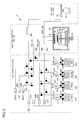
- FIG. 1 schematically illustrates the configuration of an MOCVD system 5 used for crystal growth in the present invention. A description will now be given for the details of the device configuration of the MOCVD system 5. Crystal growth materials will be described further below.
- the MOCVD system 5 comprises a gas supplying part 5A, a reaction container part 5B, and an exhaust part 5C.
- the gas supplying part 5A comprises a portion for vaporizing and supplying a metal-organic compound material gas, a portion for supplying gaseous material gas, and a transport unit provided with a function for transporting the gases.
- the metal-organic compound material gas which is liquid (or solid) at room temperature, is vaporized and fed as water vapor.
- dimethylzinc (DMZn), bis cyclopentadienyl magnesium (Cp2Mg), and triethylgallium (TEGa) are respectively used as a zinc (Zn) source, a magnesium (Mg) source, and a gallium (Ga) source.
- nitrogen gas is set to a predetermined flow rate by a flow rate adjustment device (mass flow controller) 21S and fed into a DMZn housing container 21C through a gas feed valve 21M, and the nitrogen gas is saturated with DMZn vapor.
- the DMZn-saturated nitrogen gas is fed, through an extraction valve 21E and a pressure adjustment device 21P, to a first vent pipe (hereafter, referred to as a VENT-MO line) 28V during standby for growth or to a first run pipe (hereafter, referred to as a RUN-MO line) 28R during growth.
- the internal pressure in the housing container is adjusted to a constant pressure using a pressure adjustment device 21P.
- the DMZn housing container is kept at a constant temperature by a thermostatic bath 21T.
- the other metal-organic compound material gases Cp2Mg and TEGa are also fed in a similar manner. Specifically, nitrogen gas is fed at a predetermined flow rate through a flow rate adjustment device 22S, 23S into a housing container 22C (TEGa) and 23C (Cp2Mg) housing the respective materials, and the corresponding gas is fed, through an extraction valve 22E, 23E and a pressure adjustment device 22P, 23P to a VENT-MO line (VENT1) 28V during standby for growth or to a RUN-MO line 28R during growth.
- VENT1 VENT-MO line
- a predetermined flow rate of nitrogen gas is sent through a flow rate adjustment device 24S into a housing container 24C, the nitrogen gas is saturated with water vapor, and fed, through an extraction valve 24E and a pressure adjustment device 24P, to a second vent pipe (hereafter, referred to as a VENT-Ox line) 29V during standby for growth or to a second run pipe (hereafter, referred to as a RUN-Ox line) 29R during growth.
- a second vent pipe hereafter, referred to as a VENT-Ox line
- a second run pipe hereafter, referred to as a RUN-Ox line
- Ammonia (NH 3 ) gas which is a gaseous material, is used for the p-type impurity source.
- the NH 3 gas is fed at a predetermined flow rate by the flow rate adjustment device 25S.
- the NH 3 gas is fed to the VENT-Ox line 29V during standby, and to the RUN-Ox line 29R during growth.
- the gas may also be diluted by an inert gas such as nitrogen or argon (Ar).
- the vapor of the above liquid or solid materials and the gaseous material (hereafter, referred to as material gas) is fed through the RUN-MO line 28R and the RUN-Ox line 29R to a shower head 30 of the reaction container part 5B.
- a flow rate adjustment device 20C, 20B is also provided to each of the RUN-MO line 28R and the RUN-Ox line 29R.
- the material gas is delivered by a carrier gas (nitrogen gas) to the shower head 30 mounted on the upper part of a reaction container (chamber) 39.
- the shower head 30 has a discharge surface facing the main surface (growth surface) of a substrate 10. Numerous discharge holes are arranged along the discharge surface. A configuration is adopted so that the metal-organic compound material gas and H 2 O are discharged towards the substrate 10 from individual holes.
- the shower head 30 for blowing the material gas onto the substrate 10, the substrate 10, a susceptor 19 for supporting the substrate 10, and a heater 49 for heating the susceptor 19 are installed in the reaction container 39.
- the system includes a structure with which the substrate can be heated from room temperature to about 1100°C by the heater 49.
- the substrate temperature in the present embodiment refers to the temperature of the surface of the susceptor 19 on which the substrate is placed. Specifically, in the case of MOCVD, transmission of heat-from the susceptor 19 to the substrate 10 takes place through direct contact and through the gas present between the susceptor 19 and the substrate 10. In the growth pressure range of 1kPa to 120 kPa (Pa: pascals) used in the present embodiment, the surface temperature of the substrate 10 (i.e., the growth temperature) is about 0°C to 10°C lower than the surface temperature of the susceptor 19.
- a rotation mechanism for causing the susceptor 19 to rotate is provided to the reaction container 39. More specifically, the susceptor 19 is supported by a susceptor support cylinder 48, and the susceptor support cylinder 48 is rotatably supported on a stage 41.
- a rotation motor 43 causes the susceptor support cylinder 48 to rotate, thereby causing the susceptor 19 (i.e., the substrate 10) to rotate.
- the abovementioned heater 49 is installed in the susceptor support cylinder 48.
- the exhaust part 5C comprises a container interior pressure adjustment device 51 and an exhaust pump 52, and is structured so that the container interior pressure adjustment device 51 is capable of adjusting the pressure in the reaction container 39 between 0.01 kPa to about 120 kPa.
- a zinc-based metal-organic compound that does not contain oxygen in the constituent molecule and a magnesium-based metal-organic compound having a Cp group (cyclopentadienyl group) are used as the metal-organic compound material gas (or organic metal material); and water vapor (H 2 O) is used as the oxygen source.
- a metal-organic compound that does not contain oxygen is highly reactive with H 2 O, and enables ZnO-based crystals even in regions in which the growth pressure is low or in which the VI/II ratio or the flow rate ratio (F(H2O)/F(MO) ratio) between the water vapor and the metal-organic compound (MO) is low.
- a magnesium-based metal-organic compound having a Cp group (cyclopentadienyl group) is used.
- the functional group of metal-organic compounds other than the magnesium-based metal-organic compound is preferably a chained hydrocarbon group.
- DMZn, Cp2Mg, and TEGa are used as the metal-organic compound material gas
- diethylzinc (DEZn) or another substance may be used as the Zn material.
- the magnesium-based metal-organic compound having a Cp group cyclopentadienyl group
- bisethylpentadienyl magnesium (EtCp2Mg) or another substance may be used other than Cp2Mg.
- H 2 O Water vapor
- H 2 O turns into active oxygen after supplying hydrogen through the reaction catalyst function described further below, and is therefore the most suitable oxidant for the method of the present invention.
- Trimethylgallium (TMGa), triethylgallium (TEGa), trimethylaluminum (TMAl), triethylaluminum (TEAl), triisobutylaluminum (TIBA), or another substance can be used as an impurity doping material (group III material).
- Ammonia (NH 3 ), hydrazine (Hy), monomethylhydrazine (MMHy), dimethylhydrazine (DMHy), or another substance can be used as a group V material for an impurity.
- An inert gas such as nitrogen (N 2 ), argon (Ar), xenon (Xe), or helium (He) can be used as the carrier gas.
- Nitrogen (N 2 ) is the most suitable for the carrier gas when gas purity and cost are taken into account.
- the growth catalyst function of Cp2Mg is used. Using hydrogen (H 2 ) for the carrier gas will reduce the growth catalyst effect and is therefore not desirable, but use is possible as long as the quantity is small.
- a "0.5°-offset substrate”, in which the (0001)-plane is tilted by 0.5° in the [10-10] direction (or a 0.5°-offset substrate in which the c-plane is tilted by 0.5° in the m-axis direction), and a (0001) just substrate are used for the substrate.
- a description will be given for growth of an undoped MgZnO crystal. More specifically, with regard to the first embodiment, a description will be given for growth of an undoped MgZnO crystal for a representative embodiment of the present invention (i.e., growth temperature of 850 to 900°C). With regard to the second embodiment, a description will be given for growth in an instance in which the growth temperature range is expanded, i.e., in an instance in which the growth temperature is 775 to 925°C. With regard to the third embodiment, a description will be given for growth in an instance in which the growth pressure is 2 to 40 kPa. With regard to the fourth embodiment, a description will be given for growth in instances between which the flow rate of group II (or, group-II flow rate magnification described further below) is different.
- Nitrogen (N 2 ) gas was fed from the shower head 30 to the ZnO substrate 10 from each of the RUN-MO line 28R and the RUN-Ox line 29R at a flow rate of 2 liters/min (total 4 liters
- the flow rate F(DMZn) of the DMZn was adjusted to 10 ⁇ mol/min
- H 2 O flow rate: 800 ⁇ mol/min
- the water vapor area-flow-rate FS(H2O) is 18.1 ⁇ mol ⁇ min -1 ⁇ cm -2 .
- the water vapor area-flow-rate FS(H2O) is defined as the molar flow rate per unit area of water vapor (H 2 O) fed to the ZnO substrate 10.
- the water vapor area-flow-rate FS(H2O) is a value obtained by dividing the flow rate of H 2 O by the area of the gas discharge surface (i.e., effective discharge area) of the shower head 30.
- the water vapor area-flow-rate FS(H2O) H 2 O flow rate (F(H2O))/( ⁇ ⁇ (d/2) 2 ).
- d 75.
- the growth method was described above for an example in which the growth temperature Tg is 875°C.
- the MgZnO crystal layer 12 was grown on the ZnO crystal layer 11 with different growth temperatures Tg. Specifically, crystals were grown at five different growth temperatures Tg: 850°C, 863°C, 875°C, 888°C, and 900°C. Pre-growth heat treatment, growth of the ZnO crystal layer 11, and other steps were performed in the same manner as described above. In addition, the growth pressure, growth time, and other parameters were the same as described above for growth of the MgZnO crystal layer 12, except that the growth temperatures Tg were different.
- DMZn which is a zinc-based organometal (i.e., metal-organic compound) that does not contain oxygen in the constituent molecule
- Cp2Mg which is a magnesium-based metal-organic compound having a Cp group
- water vapor (H 2 O) was used as the oxygen source
- the undoped MgZnO crystal layers 12 were grown under the following conditions.
- growth conditions such as those for the pre-growth heat treatment and the growth of the ZnO crystal layer 11 are identical to those in the first embodiment. Therefore, a description will be given below for the growth of the MgZnO crystal layer 12.
- the MgZnO crystal layer 12 was grown at a growth pressure Pg of 5 kPa and at different growth temperatures. Specifically, DMZn (flow rate: 30 ⁇ mol/min) and Cp2Mg (1.00 ⁇ mol/min) were fed from the RUN-MO line 28R, and H 2 O (flow rate: 800 ⁇ mol/min) was fed from the RUN-Ox line 29R to the ZnO substrate 10 at a flow rate, combined with the carrier gas, of 2 liters/min. The MgZnO crystal layer 12 was growth on the ZnO crystal layer 11 over a growth time of 120 minutes. Growth was performed at different growth temperatures Tg: 775°C, 825°C, 875°C, and 925°C. The layer thicknesses of the MgZnO crystal layer 12 were 60-1000 nm.
- the MgZnO crystal layer 12 was grown on the ZnO crystal layer 11 with different growth temperatures Tg.
- the water vapor area-flow-rate FS(H2O) was also identical to that in the first embodiment, at 18.1 ⁇ mol ⁇ min -1 ⁇ cm -2 .
- DMZn and Cp2Mg were used as the metal-organic (MO) materials
- water vapor (H 2 O) was used as the oxygen source
- the undoped MgZnO crystal layers 12 were grown under the following conditions.
- the ZnO crystal layer 11 was grown at a growth pressure Pg of 80 kPa and a growth temperature Tg of 775°C.
- the flow rate of DMZn was 10 ⁇ mol/min and the flow rate of H 2 O was 640 ⁇ mol/min.
- a ZnO crystal layer 11 having a thickness of approximately 0.2 ⁇ m was grown on the ZnO substrate 10 with a growth time of 24 minutes.
- the MgZnO crystal layer 12 was grown at a growth temperature Tg of 875°C.
- the flow rate of DMZn was 10 ⁇ mol/min
- the flow rate of Cp2Mg was 0.334 ⁇ mol/min
- the flow rate of H 2 O was 640 ⁇ mol/min.
- Growth was performed at five different growth pressures Pg: 2 kPa, 5 kPa, 10 kPa, 20 kPa, and 40 kPa.
- the layer thickness of the MgZnO crystal layer 12 was 20 to 30 nm.
- DMZn and Cp2Mg were used as the metal-organic (MO) materials; and water vapor (H 2 O) was used as the oxygen source, and the undoped MgZnO crystal layers 12 were grown under the following conditions.
- the heat treatment of the substrate and the method for growing the ZnO crystal layer 11 are identical to those according to the third embodiment; therefore, a description will be given below with regard to the growth of the MgZnO crystal layer 12.
- the MgZnO crystal layer 12 was grown for 120 minutes at a growth temperature Tg of 875°C and a growth pressure Pg of 5 kPa.
- the layer thickness of the MgZnO crystal layers 12 were 20-110 nm.
- DMZn and Cp2Mg were used as the metal-organic (MO) materials
- the undoped MgZnO crystal layers 12 were grown under the following conditions.
- comparative example-1 is a representative example of growth (i.e., growth temperature: 775°C)
- comparative example-2 is an example of growth in an instance in which the growth temperature range is 700-850°C
- comparative example-3 is an example of growth in an instance in which the growth pressure range is 10-40 kPa
- comparative example-4 is an example of growth in an instance in which the flow rate of the group II material are varied.
- a ZnO single-crystal substrate in which the FWHM of the XRD (100) ⁇ rocking curve is less than 40 arcsecs was used as the substrate, and the surface layer was subjected to etching treatment.
- the growth sequence was also similar to that according to the first through fourth embodiments other than the points described below. Differences with respect to the first through fourth embodiments will be mainly described below.
- the substrate temperature was 800°C and the pressure was 10 kPa.
- nitrogen gas was fed as the carrier gas from the RUN-MO line 28R at 2 liters/min.
- the flow rate F(H2O) of water vapor (H 2 O) was adjusted to 640 ⁇ mol/min, and water vapor was fed to the ZnO substrate 10 from the RUN-Ox line 29R at a flow rate, combined with the carrier gas, of 2 liters/min. Then, heat treatment was performed for 7 minutes at a substrate temperature of 800°C.
- the ZnO crystal layer 11 was grown at a growth temperature Tg of 800°C and a growth pressure Pg of 80 kPa.
- the flow rate of DMZn was 10 ⁇ mol/min, and the flow rate of Cp2Mg was 640 ⁇ mol/min.
- a ZnO crystal layer 11 having a thickness of approximately 0.2 ⁇ m was then grown on the ZnO substrate 10 over a growth time of 24 minutes.
- the MgZnO crystal layer 12 was grown at a growth temperature Tg of 775°C and a growth pressure Pg of 10 kPa.
- the flow rate of DMZn was 10 ⁇ mol/min, and the flow rate of Cp2Mg was 0.556 ⁇ mol/min.
- the MgZnO crystal layer 12 was then grown on the ZnO crystal layer 11 over a growth time of 120 minutes.
- the undoped MgZnO crystal layers 12 were grown using H 2 O flow rates of 40 ⁇ mol/min (VI/II ratio: 3.8), 80 ⁇ mol/min (VI/II ratio: 7.6), 160 ⁇ mol/min (VI/II ratio: 15.2), and 640 ⁇ mol/min (VI/II ratio: 60.6).
- the layer thickness of the MgZnO crystal layers 12 were 60-240 nm.
- the MgZnO crystal layer 12 was grown at a growth pressure Pg of 10 kPa and at different growth temperatures Tg.
- the flow rate of DMZn was 10 ⁇ mol/min
- the flow rate of Cp2Mg was 0.556 ⁇ mol/min
- the flow rate of H 2 O was 640 ⁇ mol/min.
- growth was performed at each growth temperature Tg of 700°C, 750°C, 775°C, 800°C, 825°C, and 850°C.
- An undoped MgZnO crystal layer 12 having a film thickness of 35-600 nm was then grown on the ZnO crystal layer 11 over a growth time of 120 minutes.
- the MgZnO crystal layer 12 was grown at a growth temperature Tg of 800°C and at different growth pressures Pg.
- the flow rate of DMZn was 10 ⁇ mol/min
- the flow rate of Cp2Mg was 0.556 ⁇ mol/min
- the flow rate of H 2 O was 640 ⁇ mol/min.
- growth was performed at each growth pressure Pg of 10 kPa, 20 kPa, and 40 kPa.
- Undoped MgZnO crystal layers 12 each having a film thickness of 250 nm were then grown on the ZnO crystal layer 11 over a growth time of 120 minutes.
- the MgZnO crystal layer 12 was grown at a growth temperature Tg of 775°C and a growth pressure Pg of 10 kPa, and over a growth time of 120 minutes.
- growth was performed for three instances in which the total flow rate F (II+VI) of the group-II (DMZn, Cp2Mg) flow rate and the VI group (H 2 O), i.e., the total flow rate F (II+VI) of the material gas, is different.
- the total flow rate magnification MF (II+VI) of the material gas is defined using, as a unit flow rate, the flow rate (10 ⁇ mol/min, 0.556 ⁇ mol/min, 40 ⁇ mol/min) of the abovementioned material gas (II-group and VI-group gases).
- the total flow rate magnification MF (II+IV) of the material gas is 1, and in the case of comparative example-4, MF(II+VI) is 1, 2, and 3 (also represented as ⁇ 1, x2, and ⁇ 3).
- the present invention was conceived from knowledge obtained as a result of investigation and research in relation to the growth of MgZnO-based crystals.
- a zinc-based organometal that does not contain oxygen in the constituent molecule, and a magnesium-based metal-organic compound are used as metal-organic (MO) materials; water vapor (H 2 O) is used as an oxygen source; and the MgZnO-based crystal is grown under a non-reductive atmosphere (or nitrogen atmosphere).
- a ternary mixed crystal such as Mg x Zn 1-x O
- Mg composition (x) is increased based on ZnO-crystal growth conditions
- the method for growing a MgZnO crystal disclosed in Patent Document 1 also employs such means, and the crystal quality is improved while unnecessary reaction is suppressed using reduced-pressure growth (or low-pressure growth) and a low water vapor flow rate.
- a ZnO growth system in which DMZn and water vapor are used and in which growth is performed in a nitrogen atmosphere is a non-reductive-atmosphere reaction system in which hydrogen is not present.
- DMZn which has a chain hydrocarbon, releases the chain hydrocarbon upon reacting with water vapour, even in a non-reductive atmosphere, and the generated active zinc and water vapor react and grow a ZnO crystal. At this time, the chain hydrocarbon is released (or desorbed) away from the growth surface without disrupting the ZnO crystal growth process.
- Cp2Mg has a structure in which magnesium metal is sandwiched by two Cp groups (cyclopentadienyl groups), and is therefore more chemically stable than TMGa, TMAl, or DMZn which are organometals having a chain hydrocarbon.
- Cp2Mg has a thermal decomposition temperature that is 100°C to 200°C higher than organometals having a chain hydrocarbon, and at the same time, more readily generates carbon.
- Cp2Mg is a metal-organic compound that has poor reactivity and that more readily results in residual carbon.
- the inventor of the present invention discovered the true problem with regard to growing an MgZnO crystal using Cp2Mg. Specifically, in an MgZnO growth system in which DMZn and water vapor are used, poorly reactive Cp2Mg is added, and growth is performed in a nitrogen atmosphere (or non-reductive atmosphere), the Cp groups having a cyclic structure in the Cp2Mg do not readily react with water vapor, and cyclic and polymeric chain hydrocarbons which readily remain on the growth surface are generated. In addition, in an MgZnO crystal growth system, Cp2Mg is fed at a high flow rate due to magnesium being a crystal composition element, and this effect is therefore enhanced.
- a reaction-disrupting hydrocarbon product is a cyclic hydrocarbon product derived from the Cp group having a cyclic structure, and the polymeric chain hydrocarbon polymerized during a ring-opening reaction is also a reaction-disrupting hydrocarbon product.
- These hydrocarbon products remain on the substrate surface for a long time, disrupt the MgZnO crystal growth process, generate pits (or random pits) and hillocks on the MgZnO crystal layer, and result in residual carbon.
- non-reaction-disrupting hydrocarbon products are low-molecular hydrocarbon products that have undergone a ring-opening reaction and have assumed a chain structure. These hydrocarbon products are immediately released (or desorbed) from the substrate surface and therefore do not disrupt the MgZnO crystal growth process and do not result in residual carbon.
- high-temperature growth is performed at a growth temperature equal to or higher than the upper limit temperature for ZnO single-crystal growth, i.e., a growth temperature equal to or higher than about 850°C, whereby sufficient energy for causing the Cp group to undergo a chain-opening reaction is supplied and it is made possible for the Cp group to readily turn into a chain hydrocarbon product on the substrate surface.
- a growth temperature equal to or higher than the upper limit temperature for ZnO single-crystal growth, i.e., a growth temperature equal to or higher than about 850°C
- the chain-opening reaction of the Cp group requires hydrogen element (H) for the reaction. Accordingly, water vapor is fed to the growth surface (water vapor area-flow-rate FS(H2O) : about 10 ⁇ mol ⁇ min -1 ⁇ cm -2 or greater), thereby making it possible to accelerate generation of a low-molecular chain hydrocarbon product.
- active oxygen is fed as a fragment of the above reaction to the growth surface (hereafter referred to as a "growth catalyst function"), therefore making a stable two-dimensional crystal growth (or, 2D growth) possible without a shortage of oxygen being fed, even under a high-temperature, reduced-pressure condition.
- the abovementioned "growth catalyst function" of Cp2Mg makes it possible to grow an MgZnO crystal having a Wurtzite structure.
- the method of the present invention is a crystal growth method under a unique growth condition in which even a ZnO crystal cannot be grown if Cp2Mg is not fed.
- the method of the present invention is a unique method that makes it possible to remove the growth-disrupting factor in the process of thermal decomposition of a magnesium-based metal-organic compound having a Cp group under a non-reductive atmosphere, activate the growth catalyst function, and grow a high-quality MgZnO crystal.
- the method can be said to be one that cannot be conceived as an extension of conventional growth methods.
- crystal growth layers according to the abovementioned first through fourth embodiments and comparative examples-1 through 4 will now be described in detail with reference to the accompanying drawings.
- the crystal growth layers according to the first through fourth embodiments may be referred to as EMB1 through EMB4 respectively, and the crystal growth layers of comparative examples 1 through 4 may be referred to as CMP1 through CMP4.
- the above crystal growth layers were evaluated and analyzed using the following methods.
- the surface morphology was evaluated using a differential polarization microscope, a scanning electron microscope (SEM), and an atomic force microscope (AFM).
- the crystal orientation and defect/dislocation densities were evaluated using X-ray diffraction (i.e., X-ray diffractometer (XRD)).
- the concentration of impurities in the crystal was evaluated using secondary ion mass spectrometry (SIMS).
- the crystal composition was evaluated using a 2 ⁇ measurement, and the crystal orientation was evaluated using a rocking curve measurement. More specifically, the Mg composition (x) of Mg x Zn 1-x O was evaluated using 2 ⁇ measurement of the (002)-plane, and the crystal orientation was evaluated from the half-width (full width at half maximum: FWHM) in a rocking curve measurement of the (002)-plane and the (100)-plane. If the half width is large, the amount of disruption in the orientation is large and the defect density and the dislocation density are high, and if the half width is small, the amount of disruption in the orientation is small and the defect density and/or the dislocation density are low.
- the concentration of trace impurities contained in the crystal can be analyzed and evaluated.
- a depth-direction measurement i.e., depth profile measurement
- the carrier concentration in the crystal can be measured and evaluated.
- a reverse bias voltage V is applied to a Schottky junction and the capacity C is measured. Since the tilt of V-1/C 2 is a function of the impurity concentration at the edge of the space charge layer, it is possible to obtain the impurity concentration (see Handotai Book (2nd edition), Ohm-sha, Ltd., page 265 ).
- the first embodiment is an example in which the MgZnO crystal layers 12 were grown at 850°C, 863°C, 875°C, 888°C, and 900°C, which are growth temperatures Tg for which the possibility of application is high.
- a feature of the method of the present invention is that the Mg composition (x) of Mg x Zn 1-x O (0 ⁇ x ⁇ 0.68) can be adjusted with only the growth temperature Tg while maintaining a constant growth rate and water vapor flow rate.
- FIG. 4 shows an AFM image of each of the MgZnO growth layers according to the first embodiment.
- the AFM images were measured at a visual field of 15 nm per side, 5 nm per side, and 1 nm per side.
- the only surface morphology of the MgZnO crystal layer that was observed was vertical stripes comprising terraces and steps derived from the c-plane ZnO substrate inclined by 0.5° to the m-axis direction.
- the flatness is at a satisfactory level at 2 nm or less in a 15-nm square visual field. No pits (random pits) or hillocks derived from MgZnO crystal growth were observed whatsoever.
- FIG. 5 shows differential interference microscopy images of each of the MgZnO growth layers according to the first embodiment.
- pits i.e., large pits
- the large pit densities were 6.3 ⁇ 10 3 , less than 7.0 ⁇ 10 3 , 1.4 ⁇ 10 3 , 1.5 ⁇ 10 4 , and 1.7 ⁇ 10 4 cm -2 , and were at a low level of about 10 3 to 10 4 cm -2 .
- Pits i.e., large pits
- substrate defects are a phenomenon in which pits, originating from defects and dislocations hidden in the ZnO substrate, are generated on the MgZnO crystal layer grown thereon.
- pits may be generated on the MgZnO crystal layer grown thereon.
- Such instances are also referred to as pits (i.e., large pits) derived from the ZnO substrate.
- FIG. 6A shows 2 ⁇ diffraction curves of the (0002)-plane. Diffraction peaks of the MgZnO (0002)-plane are observed at higher angle side than diffraction peaks of the ZnO (0002)-plane. As the growth temperature increases, the diffraction peaks proportionally shifts towards angle side. All diffraction curves showed a good match with results of a simulation for an MgZnO/ZnO layered structure.
- an MgZnO crystal layer is used as the barrier layer of a double-hetero structure such as a light-emitting diode (LED) and a ZnO crystal layer is used as the light-emitting layer
- a disruption to the crystal layer interface the carrier-confinement effect for the light-emitting layer will decrease and the light-emitting efficiency will decrease. Accordingly, formation of a sharp or abrupt interface is important information of a semiconductor element.
- FIG. 6B shows rocking curves of the (100)-plane of the MgZnO crystal layers.
- the half-widths (FWHMs) of the rocking curves are about 30 arcsecs in all temperature regions, and equivalent to the half-width of a ZnO substrate. Therefore, it was found that according to the present invention, twisting and tilting can be suppressed to extremely low levels and an MgZnO crystal layer having a good crystal orientation can be grown, even if the Mg composition (x) is equal to or greater than 0.17 and the layer thickness is approximately 500 nm.
- FIG. 7 shows reciprocal lattice mappings of the (105)-plane.
- the horizontal axis represents the m-axis direction
- the vertical axis represents the c-axis direction.
- the MgZnO crystal layers are layered so that the a-axis lengths are equivalent to those of a ZnO crystal layer, and the c-axis lengths increase.
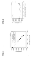
- FIG. 8 shows the relationship between the Mg composition and the c-axis length.
- the c-axis length decreases in a linear fashion (i.e., longer than that of a free-standing state). It was found that even if the Mg composition (x) is equal to or greater than 0.17 and the film thickness is approximately 500 nm, an MgZnO crystal layer can be grown on the ZnO crystal layer without there being any lattice relaxation.
- FIG. 9 shows the carrier concentration along the depth direction, obtained by CV measurement. It was found that the residual carrier concentration of the MgZnO crystal layer grown at a growth temperature of 850°C to 900°C can be kept to an extremely low value of 4.7 ⁇ 10 15 cm -3 to 1.3 ⁇ 10 16 cm -3 or less. For example, if an LED is to be manufactured, it is important that the residual carrier concentration is low for forming any of an n-type semiconductor layer, a light-emitting layer, or a p-type semiconductor layer.
- the present invention even if the growth temperature is equal to or greater than 850°C and the growth pressure is equal to or less than 5 kPa, supplying water vapor at a water vapor area-flow-rate FS(H2O) of 18.1 ⁇ mol ⁇ min -1 ⁇ cm -2 makes it possible to utilize the effect of the growth catalyst function of Cp2Mg, suppress oxygen vacancy, and keep the residual carrier concentration to 5 ⁇ 10 15 cm -3 or less.
- the carbon concentration was consistently equal to or less than the lower limit of detection according to SIMS measurement. It was found that according to the present invention, the Cp group can be desorbed as a low-molecular chain hydrocarbon from Cp2Mg, and since the standalone carbon can be desorbed as carbon dioxide due to the growth catalyst function, carbon intake during the growth process can be suppressed.
- FIG. 10A shows the relationship between the Mg composition (x) and the growth rate (GR) with respect to the growth temperature. It can be seen that there is a linearly proportional relationship between the growth temperature and the Mg composition (x), and that the Mg composition can be precisely adjusted using the growth temperature (the tilt is 0.0027°C -1 ).
- the growth rate was substantially constant (approximately 60 to 66 nm/hour) irrespective of the growth temperature Tg. Accordingly, when an MgZnO crystal having a different Mg composition (x) is layered, it is possible to control the composition (x) by changing the growth temperature Tg.
- FIG. 10B shows the relationship between the half-width FWHM of the (100) rocking curve and the carrier concentration with respect to the growth temperature. It was found that that in all growth temperature ranges, the half-width of the (100) rocking curve is constant at about 30 arcsecs, and the residual carrier density is consistently low at 2 ⁇ 10 16 cm -3 or less.
- the present invention is an excellent crystal growth method that makes it possible to grow an MgZnO crystal having an excellent flatness and crystal orientation, no residual carbon, and low residual carrier concentration, in which formation of pits (large pits) derived from the ZnO substrate and pits (random pits) and hillocks derived from MgZnO crystal growth is suppressed.
- an MgZnO crystal layer in which the Mg composition necessary for the barrier layer of the MgZnO-based semiconductor light-emitting element is no less than 0.1, the film thickness is equal to or greater than approximately 30 nm, and the a-axis length is coherent with respect to the a-axis length of a ZnO crystal. It was confirmed that the crystal formation is possible for an Mg composition (x) of up to at least 0.375 and a film thickness of up to approximately 500 nm.
- the MgZnO crystal layers were grown at growth temperatures Tg of 775°C, 825°C, 875°C, and 925°C.
- FIG. 11 shows AFM images of the MgZnO growth layers.
- the growth temperature Tg is 775°C
- film vacancy defects i.e., vacant portions or pores in the film
- there is a disruption to the vertical stripe pattern i.e., terraces and steps
- Some of the disruption remains at a growth temperature of 825°C.
- high-quality MgZnO single-crystal layers can be grown, as with the case of the first embodiment, at growth temperatures Tg of 875°C, and 925°C.
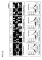
- FIG. 12 shows (100)-plane rocking curves and differential-interference microscope images of the MgZnO crystal layers for every growth temperature.
- the large-pit density derived from substrate defects was measured at an observation magnification of 50.
- the large-pit density at 775°C, 825°C, 875°C, and 925°C was countless (i.e. film vacancy defects), 6.9 ⁇ 10 4 cm -2 , 1.4 ⁇ 10 3 cm -2 , and 8.6 ⁇ 10 3 cm -2 respectively.
- the large pit density decreases for growth temperatures equal to or greater than 875°C.
- the half-width of the rocking curves was large at 49.3 arcsecs at a growth temperature of 775°C.
- the half width decreases to 30 arcsecs, and the crystal orientation improves.
- the effective growth temperature is from excess of 825°C, and taking the results of the first embodiment into consideration, about 850°C or above is the preferred growth temperature.
- the upper limit is not known, but is thought to be about 1000°C to 1100°C. Taking the heater facility costs and heater lifespan into consideration, an upper limit of about 1100°C is appropriate.
- the Mg composition (x) is preferably equal to or greater than 0.1, and further preferably equal to or greater than 0.17. This is because the growth catalyst function of Cp2Mg becomes effective and the MgZnO crystal grows in a stable manner.
- MgZnO crystal layers were grown at growth pressures Pg of 2 kPa, 5 kPa, 10 kPa, 20 kPa, and 40 kPa.
- FIG. 13 shows AFM images of the growth layers.
- the growth pressure Pg is 2 kPa or 5 kPa
- a vertical stripe pattern derived from the c-plane ZnO substrate is observed, and no pits (random pits) or hillocks derived from the MgZnO crystal growth process are observed.
- the growth pressure Pg is 10 kPa or 20 kPa
- a film vacancy defect is generated, and film formation becomes impossible at 40 kPa.
- FIG. 14 shows (100)-plane rocking curves of the MgZnO growth layers.
- the half-widths of the rocking curves are 27.6 arcsecs and 28.9 arcsecs respectively, indicating that MgZnO single-crystal layers having an excellent orientation were formed.
- the half-widths are larger at 43.6 arcsecs and 44.0 arcsecs, showing that crystal orientation has degraded.
- FIG. 15 shows the relationship between the growth pressure (Pg) and the Mg composition (x) and between the growth pressure (Pg) and the growth rate (GR). At about 5 kPa or less at which satisfactory crystal growth is observed, the Mg composition and the growth rate are not dependent on the growth pressure.
- the effective growth pressure is less than 10 kPa, and is preferably no more than about 5 kPa. If the amount of water vapor fed is sufficient, the growth catalyst function of the Cp2Mg is effective, so a high-quality MgZnO single-crystal can be grown even at 2 kPa. Crystal growth is possible at even lower pressures. Taking the depressurization facility cost into consideration, an appropriate lower limit is about 0.5 kPa.
- the MgZnO crystal growth pressure is 10 kPa
- a film vacancy defect is generated.
- the growth pressure is 10 kPa
- a thermal decomposition product of Cp2Mg is a cyclic hydrocarbon and disrupts growth, even of the growth temperature is 875°C.
- FIG. 16 shows AFM images of the growth layers.
- a vertical stripe pattern derived from the c-plane ZnO substrate is observed across the range in which the group-II flow rate magnification MF(II) is onefold to fourfold ( ⁇ 1 to ⁇ 4). No pits (random pits) derived from MgZnO crystal growth are observed.
- FIG. 17 shows (100)-plane rocking curves of the MgZnO growth layers.
- the half-widths FWHM of the rocking curves are all small at about 30 arcsecs in the range of the group-II flow rate, indicating that MgZnO single-crystal layers having an excellent crystal orientation are formed.
- FIG. 18 shows the relationship between the group II flow rate and the Mg composition (x) and between the group II flow rate and the growth rate (GR).
- the decrease in the Mg composition (x) is considered to be caused by an increase in the Cp2Mg flow rate accompanying the increase in the group-II flow rate causing an increase in the reaction catalyst function, an increase in the amount of oxygen fed to the growth surface, and an increase in the ZnO crystal component.
- the water vapor area-flow-rate FS(H2O) is 14.5 ⁇ mol ⁇ min -1 ⁇ cm -2 or 18.1 ⁇ mol ⁇ min -1 ⁇ cm -2 , then an adequate level will be achieved even if the group-II flow rate is increased up to fourfold.
- the water vapor flow rate is constant at 640 ⁇ mol/min. Therefore, with an increase in the group-II flow rate, the VI/II ratio decreases from 61.9 to 31.0 and then 20.6.
- the Mg composition (x) decreases from 0.34 to 0.30 and then 0.29.
- the water vapor flow rate is reduced to increase the Mg composition. In other words, the VI/II ratio is lowered to increase the Mg composition; whereas in the present invention, the characteristics are opposite (i.e., the Mg composition (x) decreases).
- the group-II flow rate (i.e., the molar flow rate per unit time ( ⁇ mol ⁇ min -1 )) must not exceed the water vapor flow rate (i.e., the molar flow rate per unit time ( ⁇ mol ⁇ min -1 )).
- the lower limit of the water vapor area-flow-rate is considered to be roughly 10 ⁇ mol ⁇ min -1 ⁇ cm -2 .
- the water vapor saturation rate at room temperature is 30% for 18.1, so the maximum limit at which water vapor can be fed, which is 90%, is equivalent to 54 ⁇ mol ⁇ min -1 ⁇ cm -2 .
- the crystal quality of the MgZnO crystal layer is unaffected.
- the growth temperature was 775°C, which is an appropriate conventional growth temperature for a ZnO crystal.
- the growth is performed according to a method in which the growth pressure is reduced (pressure Pg: 10 kPa) and the water vapor flow rate is low, and unnecessary reaction with the magnesium-based metal-organic compound is minimized (e.g., see Patent Document 1).
- the growth conditions for comparative example-1 are shown together in Table 1.
- Table 1 Growth conditions (comparative example-1) Water vapor flow rate ( ⁇ mol ⁇ min -1 ) 40 80 160 320 640 VI/II ratio 3.8 7.6 15.2 30.3 60.6 Mg composition (x) 0.32 0.26 0.16 0.14 0.11 Grown layer thickness (nm) 60 85 138 142 240
- FIG. 19 shows AFM images of growth layers according to comparative example-1.
- AFM images vertical stripes comprising terraces and steps derived from the 0.5°-off c-plane ZnO substrate were observed, but pits (random pits) derived from the MgZnO crystal growth and pits (large pits) derived from substrate defects were observed at high densities.
- pits random pits
- pits large pits
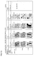
- FIG. 20 shows (100)-plane rocking curves and differential-interference microscope images of the growth layers.
- the density of pits (large pits) derived from substrate defects was measured using images having an observation magnification of 100.
- the large-pit densities were 5.6 ⁇ 10 5 , 5.9 ⁇ 10 5 , 2.9 ⁇ 10 5 , 2.2 ⁇ 10 5 , and 2.5 ⁇ 10 5 cm -2 for water vapor flow rates of 40, 80, 160, 320, and 640 ⁇ mol/min, respectively.
- the density of pits (large pits) derived from substrate defects is relatively high; i.e., on the order of the fifth power (10 5 ). This is thought to be because due to a combination of growth disruption and properties of the MgZnO crystal containing a distortion, pits are formed during the stage of MgZnO crystal growth so as to originate from the types of defects and dislocations that do not result in formation of pits in the underlying ZnO crystal layer (or grown layer).
- the half-widths of the rocking curves are about 30 arcsecs in all water vapor flow rate regions, and the crystal orientation was at a satisfactory level.
- the pressure and the water vapor flow rate are reduced to suppress unnecessary reaction with the magnesium-based metal-organic compound in order to increase the quality of the MgZnO crystal layer.
- pits derived from the MgZnO growth process i.e., random pits
- the densities of pits derived from substrate defects are in the order of the fifth power, which is higher than those according to the above embodiments.
- the Mg composition (x) decreases. More specifically, as the VI/II ratio increases from 3.8 to 60.6, the Mg composition (x) falls dramatically from 0.32 to 0.108. Additionally, the growth rate increases as the VI/II ratio increases.
- the MgZnO crystals were grown at different growth temperatures Tg.
- the growth pressure Pg was 10 kPa
- the flow rate of DMZn was 10 ⁇ mol/min
- the flow rate of Cp2Mg was 0.556 ⁇ mol/min (or 0.334 ⁇ mol/min).
- the growth conditions for comparative example-2 are shown together in Table 2.
- Table 2 Growth conditions (comparative example-2) Growth temperature Tg (°C) 700 750 775 800 825 850 Mg composition (x) 0.04 0.05 0.11 0.16 0.19 0.25 Grown layer thickness (mm) 599 386 240 119 57 26
- FIG. 21 shows AFM images of the growth layers.
- 3-dimensional growth 3D growth
- vertical stripes comprising terraces and steps derived from the 0.5°-offset c-plane ZnO substrate were observed.
- pits random pits
- the random pit density increased.
- film vacancy defects were generated.
- the low random pit density at low temperatures is considered to be because the ZnO crystal component being more readily grown causes a corresponding reduction in the effect of the thermal decomposition product of Cp2Mg or a decrease in the amount of the thermal decomposition product itself.
- the reduction in the growth layer thickness and the increase in the Mg composition at higher temperatures are considered to be due to the growth of the ZnO crystal component becoming more difficult.
- FIG. 22 shows differential-interference microscope images of the growth layers.
- the density of pits (large pits) derived from substrate defects was measured using images having an observation magnification of 100.
- the large pit densities were, for growth temperatures of 700, 750, 775, 800, 825, and 850°C, impossible to measure due to 3-dimensional growth, 4.7 ⁇ 10 5 , 2.5 ⁇ 10 5 , 1.7 ⁇ 10 5 , 1.7 ⁇ 10 4 cm -2 , and impossible to measure due to film vacancy defects, respectively.
- growth temperatures of 700°C and 850°C there is a tendency for the large pit density to be higher at lower temperatures and lower at higher temperatures. This is thought to be caused by the fact that at lower temperatures, migration of growth species during the 2-dimensional crystal growth (2D growth) process decreases, and at higher temperatures, migration of growth species in the 2-dimensional crystal growth process improves.
- FIG. 23 shows the (100)-plane rocking curves of the MgZnO crystal layers.
- the half-width FWHM of the rocking curve for a growth temperature Tg of 700, 750, 775, 800, 825, and 850°C was 81.3 arcsecs, 27.3 arcsecs with a spread at the base, 30.7 arcsecs, 38.2 arcsecs, 28.0 arcsecs, and 33.0 arcsecs with a spread at the base, respectively.
- the crystal orientation was at a satisfactory level when the growth temperature Tg was in a range of 775°C to 825°C.
- the growth temperature range according to the conventional MgZnO crystal growth method was from approximately 750°C to about 825°C.
- the data is not shown here, for a growth performed with a water vapor flow rate of 60 ⁇ mol/min, an increase in random pits and a spreading of the base of the (100)-plane rocking curve were again observed at 825°C. Accordingly, the corresponding MgZnO crystal growth method is one that can be applied to a growth temperature of 825°C or less.
- MgZnO crystals were grown at different growth pressures Pg of 10 kPa, 20 kPa, and 40 kPa.
- the growth temperature was 775°C
- the flow rate of DMZn was 10 ⁇ mol/min
- the flow rate of Cp2Mg was 0.556 ⁇ mol/min.
- FIG. 24 shows AFM images of the growth layers. Vertical stripes comprising terraces and steps derived from the 0.5°-offset c-plane ZnO substrate were observed for growth pressures Pg of 10 kPa and 20 kPa. The morphology was indefinite at a growth pressure Pg of 40 kPa.
- FIG. 25 shows differential-interference microscope images of the growth layers.
- the density of pits derived from substrate defects i.e., large pits
- the large-pit densities were at high levels of 2.5 ⁇ 10 5 , 2.4 ⁇ 10 5 , and 1.5 ⁇ 10 5 cm -2 for growth pressures of 10 kPa, 20 kPa, and 40 kPa, respectively.
- a flow-like pattern was observed on the growth surface for a growth pressure Pg of 40 kPa.
- FIG. 26 shows 2 ⁇ and (100) ⁇ rocking curves of the MgZnO crystal layers.
- the Mg composition (x) was 0.108, 0.065, and 0.00, respectively; as the growth pressure Pg increases, the Mg composition (x) decreases.
- the growth pressure Pg is at 40 kPa, the Mg composition (x) was substantially zero, and the crystal being grown was ZnO.
- the half-widths of the rocking curves were 30.7 arcsecs, 25.5 arcsecs, and 41.4 arcsecs; crystal orientation was poor for growth at 40 kPa.
- the pressure and the water vapor flow rate are reduced to suppress unnecessary reaction with the magnesium-based metal-organic compound in order to increase the quality of the MgZnO crystal layer. Accordingly, when the growth pressure Pg is 40 kPa, unnecessary reaction causes growth of a ZnO crystal layer having poor crystal orientation, the effect of suppressing the unnecessary reaction starts to take hold from 20 kPa, and MgZnO crystal growth having an Mg composition of 0.108 becomes possible at 10 kPa. However, the density of pits (large pits) derived from substrate defects are at a high level, in the order of the fifth power.
- the ZnO crystal layer grows up to at least about 40 kPa, although with poor crystal quality.
- film formation is not possible when the growth pressure Pg is 40 kPa.
- the growth method according to the present invention differs from the conventional growth method in this respect.
- comparative example-4 growth was performed for three instances between which the total flow rate F (II+VI) of the material gas (DMZn, Cp2Mg, H 2 O) differs, i.e., for instances in which the flow rate magnification MF (II+VI) is 1, 2, and 3 (i.e., ⁇ 1, ⁇ 2, and ⁇ 3).
- the growth conditions for comparative example-4 are shown together in Table 3.
- Table 3 Growth conditions (comparative example-4) Total flow rate of material gas ⁇ 1 ⁇ 2 ⁇ 3 Mg composition (x) 0.41 0.30 0.15 Grown layer thickness (mm) 36 92 143
- FIG. 27 shows AFM images of the growth layers.
- a total flow rate of the material gas of ⁇ 1 vertical stripes comprising terraces and steps derived from the 0.5°-offset c-plane ZnO substrate were observed.
- a total flow rate of the material gas of ⁇ 2 and ⁇ 3 the density of pits (random pits) derived from the MgZnO crystal growth was high, and a film vacancy defect was generated.
- FIG. 28 shows (100)-plane rocking curves of the MgZnO crystal layers.
- the half-widths FWHM of the rocking curves were 26.8 arcsecs, 31.3 arcsecs (with a wide base), and 28.7 arcsecs (with a wide base) for a total material gas flow rate of ⁇ 1, ⁇ 2, and ⁇ 3, respectively; the crystal orientation deteriorated when the material gas flow rate was increased to ⁇ 2 and ⁇ 3.
- the pressure and the water vapor flow rate are reduced to suppress unnecessary reaction with the magnesium-based metal-organic compound in order to increase the quality of the MgZnO crystal layer. Therefore, if the total material gas flow rate is increased, it becomes no longer possible to suppress unnecessary reaction, and the MgZnO crystal layer deteriorates.
- the water vapor flow rate in comparative example-4 is 80 ⁇ mol/min when the total material gas flow rate is ⁇ 2, and is still merely 120 ⁇ mol/min when the total material gas flow rate is ⁇ 3, which are less than 640 ⁇ mol/min in comparative example-2 and comparative example-3. Therefore, it is considered that the increase in the flow rate of the metal-organic material is causing unnecessary reaction.
- the MgZnO crystal growth method of the present invention differs from the conventional growth method in this respect.
- the growth temperature is equal to or greater than about 825°C, and is preferably equal to or greater than 850°C.
- the thermal decomposition product of Cp2Mg begins to be a low-molecular chain hydrocarbon at a growth temperature upward of 825°C, and the reaction stabilizes and growth of an MgZnO crystal layer having good crystallinity becomes possible at a growth temperature upward of 850°C. In particular, on the high-temperature side, growth of an MgZnO crystal took place without problem even at 925°C.
- the upper limit of the growth pressure is less than 10 kPa, and preferably equal to or less than about 5 kPa.
- Generation of a high-molecular hydrocarbon produced by thermal decomposition of Cp2Mg can be suppressed when the growth pressure is less than 10 kPa, and a growth pressure equal to or less than about 5 kPa is suited for completely suppressing the generation of a high-molecular hydrocarbon produced by thermal decomposition of Cp2Mg and obtaining an MgZnO crystal layer having a good crystal quality.
- satisfactory growth took place even at 2 kPa, and the lower limit of the pressure is not known.
- a water vapor flow rate of 10 ⁇ mol ⁇ min -1 ⁇ cm -2 is desirable, and 15 ⁇ mol ⁇ min -1 ⁇ cm -2 or greater is further preferred.
- the growth catalyst function of Cp2Mg is utilized in growing the MgZnO crystal layer; therefore, the method is not dependent on the VI/II ratio or the oxygen partial pressure. Nevertheless, the water vapor flow rate must exceed the group-II (i.e., DMZn and Cp2Mg) molar flow rate.
- FIG. 29 shows the Mg composition (x) in relation to the growth temperature Tg in the embodiments and the comparative examples described above.
- An unstable-growth temperature region at which a film vacancy defect is likely to be generated is present on the high-temperature side of the growth temperature range for the ZnO single crystal.
- growth is performed in a temperature range (hereafter referred to as "growth mode II") exceeding the temperature range in which a ZnO single-crystal can be grown (i.e., the temperature region of growth mode I) or the unstable-growth temperature region.
- growth mode II a temperature range exceeding the temperature range in which a ZnO single-crystal can be grown (i.e., the temperature region of growth mode I) or the unstable-growth temperature region.
- the method of the present invention it is possible to increase the flow rate of the group-II materials (DMZn, Cp2Mg) to increase the growth rate.
- the VI/II ratio decreases, but the Mg composition (x) does not change significantly (see, fourth embodiment).
- the crystallinity decreases and film vacancy and other problems are generated. This difference in the growth mode can be explained by the abovementioned growth catalyst function of organometals having a Cp group, effective at high temperatures, used in the method of the present invention.
- high-temperature growth is performed at a growth temperature equal to or higher than the upper limit temperature for ZnO single-crystal growth, i.e., a growth temperature equal to or higher than about 850°C, whereby sufficient energy for causing the Cp group to undergo a chain-opening reaction is supplied and it is made possible for the Cp group to readily turn into a chain hydrocarbon product on the substrate surface.
- a growth temperature equal to or higher than the upper limit temperature for ZnO single-crystal growth, i.e., a growth temperature equal to or higher than about 850°C
- having the growth pressure equal to or less than 5 kPa makes it possible to suppress a polymerization reaction during the chain-opening reaction and to generate a low-molecular chain hydrocarbon product.
- the chain-opening reaction of the Cp group requires hydrogen element (H) for the reaction.
- water vapor is fed to the growth surface (water vapor area-flow-rate FS(H2O) : about 10 ⁇ mol ⁇ min -1 ⁇ cm -2 or greater), thereby making it possible to accelerate generation of a low-molecular chain hydrocarbon product.
- the chain-opening reaction of the Cp group causes active oxygen to be fed to the growth surface (i.e., "growth catalyst function"), making a stable 2-dimensional crystal growth (2D growth) possible without a shortage of oxygen being fed, even under a high-temperature, reduced-pressure condition.
- MgZnO crystal having an excellent flatness and crystal orientation, low residual carrier concentration, and an excellent crystal quality with no residual carbon, in which formation of pits (random pits) and hillocks derived from MgZnO crystal growth is suppressed.
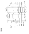
- a method for growing a Ga-doped MgZnO crystal according to a fifth embodiment will now be described in detail with reference to the crystal growth sequence shown in FIG. 30 .
- a Ga organometal (TEGa) was used as a dopant
- a ZnO crystal was grown on a ZnO substrate
- a Ga-doped MgZnO crystal was grown on the ZnO crystal.
- the substrate temperature was increased from room temperature (RT)
- nitrogen gas was fed at 2 liters/min from the RUN-MO line 28R as the carrier gas
- the flow rate F(H2O) of water vapor H 2 O was adjusted to 800 ⁇ mol/min
- the water vapor was fed to the ZnO substrate 10 from the RUN-Ox line 29R at a flow rate, combined with the carrier gas, of 2 liters/min.
- the flow rate F(DMZn) of the DMZn was adjusted to 10 ⁇ mol/min
- H 2 O flow rate: 800 ⁇ mol/min
- TEGa flow rate: 800 ⁇ mol/min
- the Ga-doping concentration can be controlled by the supply flow rate F(TEGa) of TEGa.
- the following defines the Ga flow rate ratio (hereafter also referred to as "Ng value"), which is a molar flow rate ratio of the galliuim-based organometal relative to the group-II material gas (i.e., DMZn and Cp2Mg).
- Ng value a molar flow rate ratio of the galliuim-based organometal relative to the group-II material gas (i.e., DMZn and Cp2Mg).
- the respective flow rates of DMZn and Cp2Mg are represented by F(DMZn) and F(Cp2Mg)
- Ng F TEGa / F DMZn + F Cp ⁇ 2 ⁇ Mg
- the group-II flow rate magnification MF (II) was 3 (i.e., x3).
- a magnesium-based metal-organic compound having a Cp group (Cp2Mg), a metal-organic compound that does not contain oxygen in the constituent molecule (DMZn), and water vapor (H 2 O were used; a gallium-based organometal (TEGa) was used as a dopant; and a Ga-doped MgZnO layer 12 was grown under the following conditions.
- Ga-doped MgZnO crystal growth layer of the fifth embodiment a Ga-doped MgZnO crystal was grown as comparative example-5. Growth methods such as the heat pre-treatment of the growth substrate and growth of the ZnO crystal layer 11 are identical to those according to the first embodiment; therefore, a description will be given below with regard to the growth of the MgZnO crystal layer 12. However, a heat treatment temperature of 800°C was used.
- the growth temperature Tg was 775°C, and the growth pressure was 10 kPa.
- the flow rate F(DMZn) of DMZn was 10 ⁇ mol/min
- the flow rate F(Cp2Mg) of Cp2Mg was 0.556 ⁇ mol/min.
- Growth was performed five times at different TEGa flow rates F(TEGa) of 0 nmol/min (undoped), 0.02, 0.05, 0.1, and 0.2 nmol/min.
- the Ng values (Ga flow-rate ratios) were 0 (undoped), 1.9 ⁇ 10 -6 , 4.7 ⁇ 10 -6 , 9.5 ⁇ 10 -6 , and 19 ⁇ 10 -6 , respectively.
- a Ga-doped MgZnO crystal layer having a thickness of approximately 36 to 39 nm was grown on the ZnO crystal layer 11 over a growth time of 120 minutes.
- crystal growth layers according to the fifth embodiment and comparative example-5 may be referred to as EMB5 and CMP5, respectively, in the following description.
- FIG. 31 shows the results of evaluations performed on the growth layers according to the fifth embodiment.
- the Mg composition (x) was 0.233, and the half-width FWHM of the (100)-plane rocking curve was 30.6 arcsecs ( FIG. 32B ). This FWHM of the rocking curve is equivalent to that of a ZnO substrate, and crystal orientation was regarded to be good.
- the residual carrier concentration was low, at 3.1 ⁇ 10 -16 cm -3 .
- the residual carrier concentration of the semiconductor layer be sufficiently lower than the carrier concentration to be adjusted.
- a carrier concentration of the p-type or n-type semiconductor layer of 1 ⁇ 10 17 to 1 ⁇ 10 19 cm -3 is generally used, so the residual carrier concentration is preferably equal to or less than about 5 ⁇ 10 16 cm -3 (or, equal to or less than 1/5 to 1/10 of the target carrier concentration). It shall be apparent that if the residual carrier concentration is lower, it is possible to provide the semiconductor layer so that the carrier concentration is proportional to the impurity doping amount from a lower concentration.
- the present invention is based on a method in which an MgZnO crystal can be grown at a high temperature.
- a zinc-based organometal e.g., DMZn
- a magnesium-based metal-organic compound having a Cp group e.g., a magnesium-based metal-organic compound having a Cp group
- water vapor e.g., water vapor
- growth temperature equal to or higher than 850°C
- a growth pressure of about 5 kPa or less i.e., growth temperature equal to or higher than 850°C
- a growth pressure i.e., growth temperature equal to or higher than 850°C
- a growth pressure i.e., water vapor area-flow-rate FS(H2O) equal to or greater than about 10 ⁇ mol ⁇ min -1 ⁇ cm -2 . Therefore, a growth temperature equal to or higher than 850°C is also possible for an instance in which a Ga-doped MgZn
- FIGS. 33A, 33B, 33C, and 33D show the result of measuring the 2 ⁇ rocking curve of the (002)-plane, the AFM image, the rocking curve of the (100)-plane, and CV measurement results for an instance in which the TEGa flow rate F(TEGa) is 0.3 nmol/min (Ng value: 9.7 ⁇ 10 -6 ) as a representative example of a Ga-doped MgZnO crystal layer.
- the TEGa flow rate F(TEGa) was in a range of 0.03, 0.09, 0.21, and 0.30 nmol/min (i.e., Ng values of 0.97 ⁇ 10 -6 , 2.9 x 10 -6 , 6.8 ⁇ 10 -6 , and 9.7 ⁇ 10 -6 ) .
- the surface roughness (RMS or Rq) was 2.11, 2.01, 2.75, and 1.83 nm respectively due to the effect of step bunching; however, these can be said to correspond to a satisfactory flatness, accounting for the fact that the film thicknesses are 298, 252, 228, and 254 nm respectively.
- the Mg compositions (x) were 0.176. 0.248. 0.230, and 0.230 respectively, and the FWHM values of the (100)-plane rocking curves were 31.3. 31.3, 31.8, and 31.9 arcsecs respectively for Ng values of 0.97 ⁇ 10 -6 , 2.9 ⁇ 10 -6 , 6.8 ⁇ 10 -6 , and 9.7 ⁇ 10 -6 .
- the FWHM values of the rocking curves were equivalent to those of a ZnO substrate, and the crystal orientation can be said to be good.
- the Ga-doping concentrations obtained by SIMS measurement were 2.3 ⁇ 10 17 , 1.7 ⁇ 10 18 , 2.8 ⁇ 10 18 , and 4.0 ⁇ 10 18 atoms/cm 3 .
- the carrier concentrations were 5.0 ⁇ 10 18 , 2.7 ⁇ 10 18 , 4.4 ⁇ 10 18 , and 5.9 ⁇ 10 18 cm -3 .
- FIGS. 33A, 33B, 33C, and 33D it was found that it is possible to obtain a satisfactory 2-dimensional crystal growth performance, flatness, and crystal orientation even when Ga-doping was performed up to a level corresponding to a TEGa flow rate F(TEGa) of 0.3 nmol/min (Ng value: 9.7 ⁇ 10 -6 ).
- FIG. 34 shows the SIMS depth-direction analysis (i.e., depth profile) results when the TEGa flow rate F(TEGa) was 0.3 nmol/min (Ng value: 9.7 ⁇ 10 -6 ). It was found that according to the method of the present invention, Ga exhibits a good doping profile that is equal to or less than the lower limit of detection (indicated by LM(Ga) in the drawing) in the base ZnO crystal layer 11 and rises sharply from the interface of the MgZnO crystal layer 12.
- FIG. 36 shows the relationship between the Ng value and the Ga doping concentration. It was found that when the Ng value was in a range of 0.97 ⁇ 10 -6 to 9.7 ⁇ 10 -6 at which the MgZnO crystal layer exhibits flatness, the Ga doping concentration increased in proportion to the Ng value. At an Ng value of 29 ⁇ 10 -6 , at which the MgZnO crystal layer becomes non-flat (3DG), the Ga doping concentration veers downwards off the fitting line.
- the upper limit of the Ng value at which flatness can be obtained is substantially constant at about 1 ⁇ 10 -5 irrespective of the growth temperature. Supplying TEGa at an Ng value equal to or less than this value makes it possible to obtain a Ga-doped MgZnO crystal layer exhibiting a good flatness.
- FIG. 37 shows the relationship between the Ga doping concentration and the n-type carrier concentration.
- the Ga doping concentration and the n-type carrier concentration were in a good proportional relationship. This is because the residual carrier concentration of the MgZnO crystal layer is low and gallium is functioning as a good dopant (i.e., a high activation rate).
- the n-type carrier concentration being slightly high is considered to be caused by inherent characteristics of the measurement equipment.
- the MgZnO crystal layer becomes non-flat (3DG) the Ga doping concentration decreased, and as a result the carrier concentration also decreased.
- Ng value 1 ⁇ 10 -5
- the Ga doping concentration can be adjusted by adjusting the TEGa flow rate (i.e., Ng value).
- the Ga doping concentrations were 1.8 ⁇ 10 18 , 4.0 ⁇ 10 18 , 9.1 ⁇ 10 18 , 2.9 ⁇ 10 19 , 4.7 ⁇ 10 19 , and 2.4 ⁇ 10 20 cm -3
- the n-type carrier concentrations were 2.6 ⁇ 10 18 , 5.9 ⁇ 10 18 , 1.3 ⁇ 10 19 , 2.9 ⁇ 10 19 , 6.4 ⁇ 10 19 , and 3.2 ⁇ 10 20 cm -3 .
- the upper limit of the n-type carrier concentration can be increased by increasing the growth temperature of the MgZnO crystal.
- the upper Ga doping concentration is expressed by:
- the organometal used for the n-type dopant may, instead of TEGa, be TMGa; and may also be TMA1, TEA1, or TIBA1.
- the Ng value, the upper limit doping concentration value, or the carrier concentration (or activation rate) will differ somewhat depending on the organometal used.
- FIG. 39 shows the results of evaluations performed on the undoped and Ga-doped MgZnO crystal growth layers according to a comparative example 5.
- the undoped MgZnO crystal it can be seen from the AFM image that 2-dimensional crystal growth has taken place.
- the Mg composition (x) was 0.31, and the FWHM of the (100)-plane rocking curve was 29.2 arcsecs. This rocking-curve FWHM is equivalent to that of the substrate, and crystal orientation can be said to be good.
- FIGs. 40A, 40B and 40C respectively show the results of measuring the 2 ⁇ rocking curve of the (002)-plane, the AFM image, and the rocking curve of the (100)-plane when the TEGa flow rate F(TEGa) is 0.1 nmol/min (Ng value: 9.5 ⁇ 10 -6 ). It can be seen from the AFM image that 2-dimensional crystal growth has taken place in a TEGa flow rate F(TEGa) range of 0.02, 0.05, 0.10 nmol/min (Ng values of 1.9 ⁇ 10 -6 , 4.7 ⁇ 10 - 6 , and 9.5 ⁇ 10 -6 ). The surface roughness (RMS or Rq) was 1.03, 1.33, and 0.97 nm, and the flatness was satisfactory.
- the Mg compositions (x) were 0.387, 0.397, and 0.422, and the FWHMs of the (100)-plane rocking curve were 27.1. 28.5, and 27.6 arcsecs. These rocking curve values are equivalent to those of the ZnO substrate, and crystal orientation can be said to be good.
- the Ga doping concentrations obtained by SIMS measurement were 3.0 ⁇ 10 16 , 7.0 ⁇ 10 16 , and 1.5 ⁇ 10 17 atoms/cm 3 .
- the AFM image showed a non-flat shape (3DG), and the FWHM of the (100)-plane rocking curve was 25.1, although a widening of the base was observed.
- a layered structure necessary for a semiconductor light-emitting element such as an LED cannot be formed using an MgZnO crystal layer in this state.
- FIG. 41 shows the relationship between the Ga doping concentration and the Ng value.
- the Ga doping concentration increases proportionately with respect to the Ng value in an Ng value range of 1.9 ⁇ 10 -6 to 19 ⁇ 10 -6 .
- the Ng value is at 19 ⁇ 10 -6 , the MgZnO crystal layer becomes non-flat.
- FIG. 42 shows the SIMS depth-direction analysis results when the TEGa flow rate F(TEGa) is 0.1 nmol/min (Ng value: 9.5 ⁇ 10 -6 ).
- TEGa flow rate F(TEGa) is 0.1 nmol/min (Ng value: 9.5 ⁇ 10 -6 ).
- some diffusion to the base or underlying ZnO crystal layer occurred even though the Ga concentration in the MgZnO crystal layer was low.
- Al in the ZnO has passed through the base ZnO crystal layer and diffused into the MgZnO layer. This is considered to be because Ga-doping has caused degradation of the crystal quality of the MgZnO crystal layer, Ga has diffused into the base ZnO layer, and the Al in the substrate has diffused into the MgZnO crystal layer.
- the method of the present invention is based on growth of a high-quality MgZnO crystal having a low residual carrier concentration, made possible from knowledge relating to decomposition and reaction processes of an magnesium-based metal-organic compound having a Cp group, at a growth temperature equal to or greater than the upper limit temperature for ZnO single-crystal growth.
- this method was conceived from the results of examining doping performed on a high-quality MgZnO crystal.
- a zinc-based organometal that does not contain oxygen in the constituent molecule a magnesium-based metal-organic compound having a Cp group (Cp2Mg), a dopant organometal (TEGa), and water (H 2 O are used, and high-temperature growth is performed at a growth temperature equal to or greater than the upper limit temperature for ZnO single-crystal growth, i.e., equal to or greater than about 850°C, whereby it becomes possible to grow a Ga-doped MgZnO crystal having a high doping concentration and a high quality.
- Cp2Mg magnesium-based metal-organic compound having a Cp group
- TMGa dopant organometal
- H 2 O water
- the method of the present invention uses the fact that a growth temperature equal to or greater than the upper limit temperature for ZnO single-crystal growth accelerates the chain-opening reaction of the Cp group, and the chain-opening reaction providing active oxygen to the growth surface enables stable 2-dimensional crystal growth (2D growth) and enables growth of an MgZnO crystal having an excellent crystal quality, good flatness and crystal orientation, and a low carrier concentration (i.e., the "growth catalyst function").
- Having the growth pressure equal to or less than about 5 kPa suppresses a polymerization reaction during the chain-opening reaction and enables generation of a low-molecular chain hydrocarbon product.
- an MgZnO crystal growth method of such description and adding a gallium-based organometal makes it possible to grow a Ga-doped MgZnO crystal having a high doping concentration (or high carrier concentration) and a high quality, and to grow an MgZnO crystal having an n-type carrier concentration proportional to the Ga-doping concentration. This is because the residual carrier concentration of the MgZnO crystal layer is low, and gallium functions as a good dopant (i.e., a high activation rate).
- the amount of TEGa fed is equal to or less than the upper limit Ng value (1 ⁇ 10 -5 ), it is possible to grow a Ga-doped MgZnO crystal having a high doping concentration and a high quality.
- the upper limit Ng value is substantially constant irrespective of the growth temperature, and the doping concentration (carrier concentration) can be changed by changing the growth temperature.
- the doping concentration carrier concentration
- having a high growth temperature enhances the gallium element intake rate of the crystal, making high-concentration doping possible.
- the present invention it is possible to grow a Ga-doped MgZnO crystal having a good flatness and crystal orientation, suppressed formation of random pits and hillocks, and a high carrier concentration and a high quality.
Landscapes
- Chemical & Material Sciences (AREA)
- Engineering & Computer Science (AREA)
- Materials Engineering (AREA)
- Metallurgy (AREA)
- Organic Chemistry (AREA)
- General Chemical & Material Sciences (AREA)
- Chemical Kinetics & Catalysis (AREA)
- Crystallography & Structural Chemistry (AREA)
- Inorganic Chemistry (AREA)
- Mechanical Engineering (AREA)
- Chemical Vapour Deposition (AREA)
Applications Claiming Priority (2)
| Application Number | Priority Date | Filing Date | Title |
|---|---|---|---|
| JP2012066855A JP5893980B2 (ja) | 2012-03-23 | 2012-03-23 | マグネシウム・酸化亜鉛系結晶の成長方法 |
| JP2012066858A JP5893981B2 (ja) | 2012-03-23 | 2012-03-23 | マグネシウム・酸化亜鉛系結晶の成長方法 |
Publications (1)
| Publication Number | Publication Date |
|---|---|
| EP2641996A1 true EP2641996A1 (fr) | 2013-09-25 |
Family
ID=47912877
Family Applications (1)
| Application Number | Title | Priority Date | Filing Date |
|---|---|---|---|
| EP13001444.2A Withdrawn EP2641996A1 (fr) | 2012-03-23 | 2013-03-20 | Procédé de croissance de cristaux à base de magnésium-zinc-oxyde |
Country Status (2)
| Country | Link |
|---|---|
| US (1) | US20130269600A1 (fr) |
| EP (1) | EP2641996A1 (fr) |
Cited By (3)
| Publication number | Priority date | Publication date | Assignee | Title |
|---|---|---|---|---|
| CN108922930A (zh) * | 2018-07-12 | 2018-11-30 | 中国科学院长春光学精密机械与物理研究所 | 一种ZnMgO紫外探测器 |
| CN108962732A (zh) * | 2018-07-12 | 2018-12-07 | 中国科学院长春光学精密机械与物理研究所 | 一种ZnMgO薄膜及其制备方法 |
| US11427499B2 (en) | 2017-11-29 | 2022-08-30 | Pilkington Group Limited | Process for depositing a layer |
Families Citing this family (3)
| Publication number | Priority date | Publication date | Assignee | Title |
|---|---|---|---|---|
| KR102680861B1 (ko) * | 2016-12-15 | 2024-07-03 | 삼성전자주식회사 | 질화 갈륨 기판의 제조 방법 |
| AU2018246251A1 (en) * | 2017-03-29 | 2019-10-17 | Ih Ip Holdings Limited | Methods for increasing hydrogen trapping vacancies in materials |
| KR102520541B1 (ko) * | 2018-02-14 | 2023-04-10 | 엘지디스플레이 주식회사 | 산화물 박막의 제조 장치와 제조 방법 및 그 산화물 박막을 포함하는 디스플레이 장치 |
Citations (10)
| Publication number | Priority date | Publication date | Assignee | Title |
|---|---|---|---|---|
| JP2006073726A (ja) | 2004-09-01 | 2006-03-16 | Shin Etsu Handotai Co Ltd | 化合物半導体素子の製造方法 |
| JP2008243987A (ja) | 2007-03-26 | 2008-10-09 | Tokyo Univ Of Agriculture & Technology | 酸化亜鉛系半導体の製造方法及び酸化亜鉛系半導体の製造装置 |
| JP2008244011A (ja) | 2007-03-26 | 2008-10-09 | National Institute For Materials Science | 酸化亜鉛薄膜の形成方法 |
| WO2009143226A1 (fr) * | 2008-05-21 | 2009-11-26 | Lumenz, Inc. | Couches épitaxiales à base d'oxyde de zinc et dispositifs |
| JP2010010629A (ja) | 2008-06-30 | 2010-01-14 | Tokyo Univ Of Agriculture & Technology | ホモエピタキシャル成長方法、ホモエピタキシャル結晶構造、ホモエピタキシャル結晶成長装置および半導体装置 |
| US20100064966A1 (en) * | 2008-09-16 | 2010-03-18 | Stanley Electric Co., Ltd. | Method of growing zinc-oxide-based semiconductor and method of manufacturing semiconductor light emitting device |
| WO2010033910A1 (fr) * | 2008-09-19 | 2010-03-25 | Lumenz Llc | Dispositifs électroluminescents minces et leurs procédés de fabrication |
| US20100295039A1 (en) * | 2009-05-25 | 2010-11-25 | Stanley Electric Co., Ltd. | Method for growing zinc-oxide-based semiconductor device and method for manufacturing semiconductor light emitting device |
| JP2012066855A (ja) | 2010-09-24 | 2012-04-05 | Toppan Printing Co Ltd | 紙製コップ形飲料容器 |
| JP2012066858A (ja) | 2010-09-26 | 2012-04-05 | Ishikawa Kk | バルブ付紙袋 |
-
2013
- 2013-03-20 EP EP13001444.2A patent/EP2641996A1/fr not_active Withdrawn
- 2013-03-22 US US13/849,409 patent/US20130269600A1/en not_active Abandoned
Patent Citations (11)
| Publication number | Priority date | Publication date | Assignee | Title |
|---|---|---|---|---|
| JP2006073726A (ja) | 2004-09-01 | 2006-03-16 | Shin Etsu Handotai Co Ltd | 化合物半導体素子の製造方法 |
| JP2008243987A (ja) | 2007-03-26 | 2008-10-09 | Tokyo Univ Of Agriculture & Technology | 酸化亜鉛系半導体の製造方法及び酸化亜鉛系半導体の製造装置 |
| JP2008244011A (ja) | 2007-03-26 | 2008-10-09 | National Institute For Materials Science | 酸化亜鉛薄膜の形成方法 |
| WO2009143226A1 (fr) * | 2008-05-21 | 2009-11-26 | Lumenz, Inc. | Couches épitaxiales à base d'oxyde de zinc et dispositifs |
| JP2010010629A (ja) | 2008-06-30 | 2010-01-14 | Tokyo Univ Of Agriculture & Technology | ホモエピタキシャル成長方法、ホモエピタキシャル結晶構造、ホモエピタキシャル結晶成長装置および半導体装置 |
| US20100064966A1 (en) * | 2008-09-16 | 2010-03-18 | Stanley Electric Co., Ltd. | Method of growing zinc-oxide-based semiconductor and method of manufacturing semiconductor light emitting device |
| WO2010033910A1 (fr) * | 2008-09-19 | 2010-03-25 | Lumenz Llc | Dispositifs électroluminescents minces et leurs procédés de fabrication |
| US20100295039A1 (en) * | 2009-05-25 | 2010-11-25 | Stanley Electric Co., Ltd. | Method for growing zinc-oxide-based semiconductor device and method for manufacturing semiconductor light emitting device |
| JP2010272807A (ja) | 2009-05-25 | 2010-12-02 | Stanley Electric Co Ltd | 酸化亜鉛系半導体の成長方法及び半導体発光素子の製造方法 |
| JP2012066855A (ja) | 2010-09-24 | 2012-04-05 | Toppan Printing Co Ltd | 紙製コップ形飲料容器 |
| JP2012066858A (ja) | 2010-09-26 | 2012-04-05 | Ishikawa Kk | バルブ付紙袋 |
Non-Patent Citations (1)
| Title |
|---|
| "Handotai Book", OHM-SHA, LTD., pages: 265 |
Cited By (4)
| Publication number | Priority date | Publication date | Assignee | Title |
|---|---|---|---|---|
| US11427499B2 (en) | 2017-11-29 | 2022-08-30 | Pilkington Group Limited | Process for depositing a layer |
| CN108922930A (zh) * | 2018-07-12 | 2018-11-30 | 中国科学院长春光学精密机械与物理研究所 | 一种ZnMgO紫外探测器 |
| CN108962732A (zh) * | 2018-07-12 | 2018-12-07 | 中国科学院长春光学精密机械与物理研究所 | 一种ZnMgO薄膜及其制备方法 |
| CN108962732B (zh) * | 2018-07-12 | 2020-05-12 | 中国科学院长春光学精密机械与物理研究所 | 一种ZnMgO薄膜及其制备方法 |
Also Published As
| Publication number | Publication date |
|---|---|
| US20130269600A1 (en) | 2013-10-17 |
Similar Documents
| Publication | Publication Date | Title |
|---|---|---|
| US11982016B2 (en) | Method for growing beta-Ga2O3-based single crystal film, and crystalline layered structure | |
| US11651959B2 (en) | Method and system for group IIIA nitride growth | |
| TWI433313B (zh) | 藉氫化物汽相磊晶術生長平面、非極性a-平面氮化鎵 | |
| US20180274088A1 (en) | Method for manufacturing nitride semiconductor substrate | |
| CA2678488C (fr) | Procede de fabrication d'un cristal de nitrure d'element du groupe iii | |
| US8530272B2 (en) | Method for growing zinc-oxide-based semiconductor device and method for manufacturing semiconductor light emitting device | |
| EP2641996A1 (fr) | Procédé de croissance de cristaux à base de magnésium-zinc-oxyde | |
| US9896780B2 (en) | Method for pretreatment of base substrate and method for manufacturing layered body using pretreated base substrate | |
| JP5411681B2 (ja) | 酸化亜鉛系半導体の成長方法及び半導体発光素子の製造方法 | |
| WO2004019390A2 (fr) | Tirage mbe d'une couche d'algan ou d'une structure multicouche d'algan | |
| US12606934B2 (en) | Group III nitride crystal, group III nitride semiconductor, group III nitride substrate, and method for producing group III nitride crystal | |
| JP7296614B2 (ja) | 窒化物半導体の製造方法、窒化物半導体、及び発光素子 | |
| JPH09107124A (ja) | 3−5族化合物半導体の製造方法 | |
| JP5893981B2 (ja) | マグネシウム・酸化亜鉛系結晶の成長方法 | |
| Traversa et al. | Effects of substrate treatment and growth conditions on structure, morphology, and luminescence of homoepitaxial ZnTe deposited by metalorganic vapor phase epitaxy | |
| WO2004051718A1 (fr) | Semi-conducteur compose d'elements des groupes 3-5 et son procede de fabrication | |
| JP5893980B2 (ja) | マグネシウム・酸化亜鉛系結晶の成長方法 | |
| JP5647881B2 (ja) | 酸化亜鉛系半導体の成長方法 | |
| Cantwell et al. | Vapor transport growth of ZnO substrates and homoepitaxy of ZnO device layers | |
| Gergova | Growth and characterization of group III-nitrides by migration enhanced afterglow epitaxy |
Legal Events
| Date | Code | Title | Description |
|---|---|---|---|
| PUAI | Public reference made under article 153(3) epc to a published international application that has entered the european phase |
Free format text: ORIGINAL CODE: 0009012 |
|
| AK | Designated contracting states |
Kind code of ref document: A1 Designated state(s): AL AT BE BG CH CY CZ DE DK EE ES FI FR GB GR HR HU IE IS IT LI LT LU LV MC MK MT NL NO PL PT RO RS SE SI SK SM TR |
|
| AX | Request for extension of the european patent |
Extension state: BA ME |
|
| 17P | Request for examination filed |
Effective date: 20140325 |
|
| RBV | Designated contracting states (corrected) |
Designated state(s): AL AT BE BG CH CY CZ DE DK EE ES FI FR GB GR HR HU IE IS IT LI LT LU LV MC MK MT NL NO PL PT RO RS SE SI SK SM TR |
|
| 17Q | First examination report despatched |
Effective date: 20150825 |
|
| STAA | Information on the status of an ep patent application or granted ep patent |
Free format text: STATUS: THE APPLICATION IS DEEMED TO BE WITHDRAWN |
|
| 18D | Application deemed to be withdrawn |
Effective date: 20160105 |