EP2642341A2 - Méthode de fabrication d'un dispositif pour le traitement de molécules individuelles - Google Patents
Méthode de fabrication d'un dispositif pour le traitement de molécules individuelles Download PDFInfo
- Publication number
- EP2642341A2 EP2642341A2 EP12174261.3A EP12174261A EP2642341A2 EP 2642341 A2 EP2642341 A2 EP 2642341A2 EP 12174261 A EP12174261 A EP 12174261A EP 2642341 A2 EP2642341 A2 EP 2642341A2
- Authority
- EP
- European Patent Office
- Prior art keywords
- layer
- self
- resist
- processing
- aperture
- Prior art date
- Legal status (The legal status is an assumption and is not a legal conclusion. Google has not performed a legal analysis and makes no representation as to the accuracy of the status listed.)
- Ceased
Links
Images








Classifications
-
- G—PHYSICS
- G01—MEASURING; TESTING
- G01N—INVESTIGATING OR ANALYSING MATERIALS BY DETERMINING THEIR CHEMICAL OR PHYSICAL PROPERTIES
- G01N33/00—Investigating or analysing materials by specific methods not covered by groups G01N1/00 - G01N31/00
- G01N33/48—Biological material, e.g. blood, urine; Haemocytometers
- G01N33/483—Physical analysis of biological material
- G01N33/487—Physical analysis of biological material of liquid biological material
- G01N33/48707—Physical analysis of biological material of liquid biological material by electrical means
- G01N33/48721—Investigating individual macromolecules, e.g. by translocation through nanopores
-
- B—PERFORMING OPERATIONS; TRANSPORTING
- B81—MICROSTRUCTURAL TECHNOLOGY
- B81C—PROCESSES OR APPARATUS SPECIALLY ADAPTED FOR THE MANUFACTURE OR TREATMENT OF MICROSTRUCTURAL DEVICES OR SYSTEMS
- B81C1/00—Manufacture or treatment of devices or systems in or on a substrate
- B81C1/00015—Manufacture or treatment of devices or systems in or on a substrate for manufacturing microsystems
- B81C1/00023—Manufacture or treatment of devices or systems in or on a substrate for manufacturing microsystems without movable or flexible elements
- B81C1/00087—Holes
-
- B—PERFORMING OPERATIONS; TRANSPORTING
- B82—NANOTECHNOLOGY
- B82Y—SPECIFIC USES OR APPLICATIONS OF NANOSTRUCTURES; MEASUREMENT OR ANALYSIS OF NANOSTRUCTURES; MANUFACTURE OR TREATMENT OF NANOSTRUCTURES
- B82Y30/00—Nanotechnology for materials or surface science, e.g. nanocomposites
-
- G—PHYSICS
- G03—PHOTOGRAPHY; CINEMATOGRAPHY; ANALOGOUS TECHNIQUES USING WAVES OTHER THAN OPTICAL WAVES; ELECTROGRAPHY; HOLOGRAPHY
- G03F—PHOTOMECHANICAL PRODUCTION OF TEXTURED OR PATTERNED SURFACES, e.g. FOR PRINTING, FOR PROCESSING OF SEMICONDUCTOR DEVICES; MATERIALS THEREFOR; ORIGINALS THEREFOR; APPARATUS SPECIALLY ADAPTED THEREFOR
- G03F7/00—Photomechanical, e.g. photolithographic, production of textured or patterned surfaces, e.g. printing surfaces; Materials therefor, e.g. comprising photoresists; Apparatus specially adapted therefor
- G03F7/0002—Lithographic processes using patterning methods other than those involving the exposure to radiation, e.g. by stamping
-
- B—PERFORMING OPERATIONS; TRANSPORTING
- B81—MICROSTRUCTURAL TECHNOLOGY
- B81C—PROCESSES OR APPARATUS SPECIALLY ADAPTED FOR THE MANUFACTURE OR TREATMENT OF MICROSTRUCTURAL DEVICES OR SYSTEMS
- B81C2201/00—Manufacture or treatment of microstructural devices or systems
- B81C2201/01—Manufacture or treatment of microstructural devices or systems in or on a substrate
- B81C2201/0101—Shaping material; Structuring the bulk substrate or layers on the substrate; Film patterning
- B81C2201/0147—Film patterning
- B81C2201/0149—Forming nanoscale microstructures using auto-arranging or self-assembling material
Definitions
- the invention relates to a method for manufacturing an apparatus that can be used for the processing of single molecules.
- the US 2010/0327847 A1 discloses a solid state molecular sensor having an aperture extending through a graphene layer. A change in an electrical characteristic of said layer is measured when a molecule passes through said aperture.
- One drawback of this sensor is the high electrical conductivity of the graphene layer, compared to which conductivity changes induced by a molecule are very small.
- nucleic acids shall most generally comprise molecules (e.g. DNA, RNA) that contain naturally and/or non-naturally occurring nucleotides or modifications thereof as well as LNA (locked nucleic acids) and PNA (peptide nucleic acids).
- LNA locked nucleic acids
- PNA peptide nucleic acids
- the "processing" of these molecules may comprise their physical and/or chemical transformation or alternation. In many important applications, the processing will however be a sensing, particularly serving for the detection of different sections of a molecule. Thus it may for example be possible to sequence ss-DNA, ds-DNA or the like.
- the manufacturing method comprises the following steps, which are preferably executed in the listed order, but which may also be executed in any other order that is appropriate:
- the processing layer may optionally comprise two or more sub-layers of different materials and/or structures. Moreover, the processing layer may be homogenous or (e.g. geometrically or chemically) structured. As the term "layer” indicates, the processing layer will typically have a sheet-like geometry with a width and length that are considerably larger than its thickness.
- the described method has the advantage that it allows for the generation of small apertures by which single molecules can reliably be processed. This is achieved by exploiting the self-assembling characteristics of certain resists, which yield structures of nanometer-sizes that are appropriate for the intended purposes.
- the manufacturing method allows for a mass production because a multitude of apertures can be generated in parallel this way. This is a considerable advantage over production methods as for example e-beam lithography by which apertures of comparable small sizes can only be produced sequentially.
- the manufacturing method comprises the additional step "e)" of removing the remaining self-assembling resist from the processing layer.
- the self-assembling resist serves solely as an intermediate mask during the production of the apparatus.
- the processing layer may optionally be pre-treated before the deposition of the self-assembling resist in step b), wherein this pre-treatment is such that it affects the resulting pattern of phases that is formed by the self-assembling resist.
- this pre-treatment is such that it affects the resulting pattern of phases that is formed by the self-assembling resist.
- the formation of the pattern can be controlled or adjusted as required.
- the aforementioned pre-treatment may for example comprise the provision of the processing layer with a particular (optionally structured) surface chemistry.
- the pre-treatment of the processing layer comprises the deposition of a resist on the processing layer and the patterning of this resist.
- this resist will in the following be called "primary resist”.
- the primary resist With the patterning of the primary resist, confined areas like trenches or holes may for example be generated on the surface of the processing layer in which the self-assembling resist can develop specific patterns of phases.
- the primary resist may thus serve as a kind of framework or matrix for the self-assembling resist.
- the aforementioned patterning of the primary resist may particularly be done by optical lithography and/or by e-beam lithography.
- Optical lithography advantageously allows for the parallel processing of large areas in one step, providing them with a coarse structure to which the self-assembling resist can later add a fine structure.
- the steps b), c), and d) - i.e. the deposition of a self-assembling resist, the removal of one phase of this resist, and the generation of at least one aperture - may be executed a first time with respect to a first processing layer and a second time with respect to a second processing layer, wherein said first and second processing layers may be identical or different.
- further related steps e.g. the removal of remaining self-assembling resist and/or the deposition of a (structured) primary resist, may be repeated, too.
- the processing steps are executed with the same processing layer, this will result in the generation of apertures in said layer according to the different patterns of the applied two self-assembling resists.
- the processing steps are executed with different processing layers, the resulting apertures will be located in different layers and may optionally also have different patterns.
- the second processing layer comprises the first processing layer. This entails that the later produced apertures will also penetrate the first processing layer that comprises already the first produced apertures.
- the patterns of the self-assembling resists that are applied in the first and the second execution of the above steps may preferably be different in alignment and/or geometry. This allows for the generation of elaborate aperture structures.
- the first and the second pattern each comprise stripes of (at least) one phase, wherein the stripes of the different patterns are oblique to each other.
- the apertures that are generated with the self-assembling resists will then be oblique slits.
- the oblique slits are in different layers and overlap, thus commonly constituting a smaller aperture in the region of their overlap.
- the pattern that is generated by the phases of the self-assembling resist may comprise stripes or cylinders of one phase. Stripes allow for the generation of trenches, while cylinders enable the generation of round holes in the processing layer.
- the self-assembling resist may comprise a block copolymer.
- the macromolecules of the self-assembling resist then consist of two (or a more) monomers, wherein sections consisting of only one type of monomer constitute "blocks" and wherein different blocks alternate.
- the corresponding blocks will have particular chemical and/or physical properties that enable the (self-) arrangement of the macromolecules in specific patterns.
- the processing layer may particularly comprise a non-conductive sub-layer or material, for example SiO 2 , SiN x or h-BN. Additionally or alternatively, it may comprise an electrically conductive sub-layer or material.
- the aforementioned electrically conductive sub-layer or material may particularly comprise graphene or from graphene derived materials such as graphyne (cf D. Malko, C. Neiss, F. Vinesc, and A. Görling, Phys Rev. Lett. 108, 086804 (2012 )).
- Graphene (or a derivative) is a preferred material due to its favorable electrical and mechanical properties at nano-scale dimensions.
- the graphene (or its derivative) may be present in five monolayers or less, preferably two monolayers, or more preferably in a single monolayer. Thus a favorable low thickness can be achieved.
- an additional layer may be deposited at least partially on the processing layer, wherein said additional layer may particularly be a conductive or a non-conductive layer.
- An additional layer may be advantageous in that it increases the mechanical stability, provides an electrical insulation (if it is non-conductive), and helps to orient processed single molecules appropriately.
- an additional layer may constitute a further processing layer or a part thereof in a further application of the structuring steps of the invention.
- Such components may particularly be realized by an electrical circuit adapted to control interactions with the molecules passing through the aperture.
- a circuit is preferably connected to the processing layer and/or a sub-layer thereof.
- the aperture may be embedded in a microfluidic circuit ensuring the transfer of the molecules of interest, e.g. DNA fragments, to the aperture.
- the aforementioned circuit may be adapted to sense conductivity changes which occur when a molecule or different portions of a molecule pass through the aperture.
- the aforementioned circuit may be adapted to sense conductivity changes which occur when a molecule or different portions of a molecule pass through the aperture.
- a plurality of apertures is provided.
- these apertures are provided on/in a common carrier or substrate.
- the invention further comprises an apparatus for the processing of single molecules, wherein said apparatus is obtainable by any of the methods described above.
- the apparatus can be produced by (a) providing a "processing layer", (b) depositing a self-assembling resist on said processing layer and letting it self-assemble into a pattern of two phases, (c) removing selectively one phase of the self-assembling resist, and (d) generating at least one aperture in the processing layer through the mask of the remaining self-assembling resist.
- Other manufacturing methods for the apparatus comprise for example the generation of apertures by e-beam lithography.
- the aforementioned apparatus may comprise:
- the US 2010/0327847 A1 describes the use of a graphene layer/electrode in nanopore sequencing. It is proposed in this patent that a nanopore is embedded in the graphene, leaving areas besides the nanopore.
- a crossed-slit (graphene) device can be used.
- FIGS 1 and 2 schematically sketch an exemplary apparatus 100 that is designed according to the aforementioned concept.
- the central components of this apparatus 100 are two layers, namely:
- the first slit 111 and the second slit 121 are oriented perpendicular with respect to each other and overlap partially in a region of a (rectangular) aperture A through which single molecules M can pass.
- the apparatus 100 further comprises contacts 130a, 130b disposed on the top layer parts 120a, 120b. Via these contacts, the top layer is connected to a circuit 140.
- This circuit 140 is adapted to sense electrical interactions that take place between the top layer parts 120a and 120b and single molecules passing through an aperture A.
- Figures 3 and 4 show in similar views a second apparatus 200 that is designed analogously to the apparatus 100.
- the only difference is that several (here four) parallel slits 211 in the bottom layer 210 are crossed by several (here three) perpendicular slits 221 in the top layer 220.
- the various slits may have the same widths wt or wb, respectively, or different widths. If a molecule M passes through one of the apertures A that are generated in this way, an electrical signal is sensed via the adjacent parts 220a, 220b or 220b, 220c or 220c, 220d of the top layer 220.
- the described crossed nano-slit devices 100, 200 have the following advantages over known devices to perform transverse-conductance based sequencing using graphene nanopores:
- An apparatus of the kind described above requires the generation of apertures or slits with a width (wt, wb) in the order of a few nm.
- a width of about 1-2 nm is for example required based on the calculations performed by Postma (above) of the tunneling current.
- Such slits might be generated by e-beam lithography, but this technology is not ideal for fast wafer scale manufacture of nanopore sequencing devices.
- optical techniques currently do not offer the 1-2 nm width required to make proper nano-slits.
- Block copolymers have the ability to self-assemble into highly regular patterns with dense features at length scales down to about 5 nm (cf. Black et al., IBM J. Res. & Dev. 2007, 51(5), 605 ).
- the most commonly used block copolymers, diblock copolymers are made of two blocks of polymerized monomers of different type, which are covalently linked together in a linear fashion.
- the block copolymer self-assembly process is driven by the minimization of free energy and is dependent upon the Flory-Huggins interactions parameter (measure for immiscibility of the different blocks).
- Block copolymers can form many different phases, mainly dependent upon the volume fractions of the blocks.
- the self-assembly features can be aligned and directed by allowing the self-assembly to take place in between pre-patterned topographical features (grapho-epitaxy).
- Typical block copolymers to be used in relation to this invention comprise PS- b -PMMA (Poly(styrene- b -methyl-methacrylate)), PS- b -PDMS (Poly(styrene- b -dimethylsiloxane), PS- b -PEO (Poly(styrene- b -ethyleneoxide), PS- b -PVP (Poly(styrene- b -vinylpyridine), PMMA- b -PDMS (Poly(methylmethacrylate- b -dimethylsiloxane), PS- b -PI (Poly(styrene- b -isoprene), or other block copolymers that form self-assembled patterns.
- PS- b -PMMA Poly(styrene- b -methyl-methacrylate)
- PS- b -PDMS Poly(styrene- b
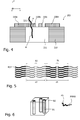
- Figure 5 schematically illustrates a laminar pattern formed by self-assemblage of block copolymer macromolecules BCP.
- the macromolecules BCP comprise an alternating sequence of blocks B1 and B2, wherein the first blocks B1 consist of a first type of monomer and the second blocks B2 consist of a different second type of monomer.
- the length of the different blocks B1, B2 i.e. the number of contained monomers
- the macromolecules BCP have at least approximately an identical spatial configuration which implies that they can self-assemble into a pattern in which equal blocks of different macromolecules BCP come close to each other. In the example shown, this results in a laminar pattern with stripes or "phases" of width d1 and d2, respectively.
- a pattern of this kind may for example be produced with block copolymers with volume fractions of 50% PS and 50% PMMA.
- Figure 6 illustrates another self-assembled pattern of a block copolymer, wherein said pattern comprises cylinders B1 of a first phase embedded in a second phase B2.
- a pattern of this kind may for example be produced with a block copolymer with volume fractions of 30% PMMA (as first phase B1) and 70% PS (as second phase B2).
- Figures 7-12 show schematically consecutive basic steps of a manufacturing method according to the invention.
- the manufacturing method starts with the provision of a "processing layer” 110 (or more generally referred to as "PL"), which can for example be the non-conductive substrate (e.g. SiO 2 ) of the apparatus 100 of Figures 1 and 2 .
- a processing layer 110 (or more generally referred to as "PL"), which can for example be the non-conductive substrate (e.g. SiO 2 ) of the apparatus 100 of Figures 1 and 2 .
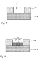
- a "primary resist” 151 has been deposited and already been patterned, for example by optical lithography. This patterning results in walls of the primary resist 151 that confine a trench or channel between them.
- Figure 8 shows the next step, in which a self-assembling resist 155 has been deposited in the aforementioned trench.
- the self-assembling resist 155 has self-assembled into a pattern of a first phase 155a and a second phase 155b.
- the pattern is assumed to be a laminar pattern of three stripes extending in y-direction.
- the central first phase 155a of the self-assembling resist has been removed, for example by selective etching, in which the etch resistance of the second phase 155b is significantly higher compared to that of the first phase 155a. Accordingly, only a pattern with parallel stripes of the second phase 155b remains.
- the first phase 155a can be removed selectively by photolytic degradation and subsequent dissolution of the degradation products.
- PMMA may for example degrade faster upon UV exposure (e.g. using 256 nm light) than PS. This method would be very suited since the whole wafer could be exposed to UV at once. Thus there is no need for using high resolution tools.
- the aforementioned remainder of the second phase 155b has been used as a mask through which the processing layer 110 has been etched to generate an aperture A, which is a slit in this case.
- the slit A may later serve as aperture through which single molecules can pass.
- the pattern formed by the aforementioned remainder of the second phase is transferred in an underlying hardmask layer (e.g. silicon oxide or silicon nitride) that is subsequently used to etch processing layer 110 to generate apertures A.
- an underlying hardmask layer e.g. silicon oxide or silicon nitride
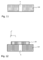
- FIG 11 an (optional) additional step is shown in which the remainder 155b of the self-assembling resist and the primary resist 151 have been removed. Accordingly, only the processing layer 110 with the aperture A remains. It is however also possible to leave this step out, for example if the remaining resist on the processing layer is desired as an electrical insulation.
- Figure 12 shows the next step if the apparatus 100 of Figures 1 and 2 shall be produced.
- a top layer 120 e.g. of graphene
- an aperture or slit in a direction perpendicular to the aperture A of the substrate 110 i.e. in x-direction
- Figures 7-11 show the practically important case in which there is just one central stripe 155a of a first phase of a self-assembling resist
- An approach of this kind might for example be used to produce the apparatus 200 of Figures 3 and 4 .
- a disposable has to be made of millions of nanopores in parallel, to process the DNA for a single diagnostics test as the DNA of a single cell is comprised of 3 ⁇ 10 9 bases (if just a fraction of the genome shall be sequenced, fewer nanopores may suffice).
- the described manufacturing procedure is advantageous as it allows using optical lithography. According to the state of the art of optical lithography in 2011, only features of about 22 nm size can be made by this technique. However, from a manufacturing standpoint using optical lithography would be ideal. It has two key advantages over e-beam lithography, namely that:
- lines could be created with on average 9 nm line width, using a PS-b-PMMA block copolymer spun cast from a toluene solution. The sample was annealed for at 200°C in an oven to facilitate the self-assembly of the block copolymers.
- the aforementioned pattern could be used as an etch pattern to etch in the underlying dielectric layers such as SiO 2 , SiN x , or hexagonal boron nitride (h-BN, which closely matches to the graphene structure). Etching subsequently in a graphene layer is straightforward as a few seconds in an O 2 -plasma is sufficient to etch a graphene single or double layer away.
- h-BN hexagonal boron nitride
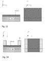
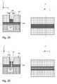
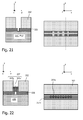
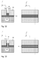
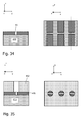
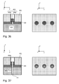
- Figures 13-24 illustrate another manufacturing procedure in which the basic steps described above ( Figures 7-11 ) are repeated three times with different parameters and objects.
- the right hand sides of Figures 13-24 all show a top view of the intermediate products, while the left hand sides of these Figures show a sectional view along the respective dashed line.
- the procedure starts with the provision of a first processing layer 320 (or "PL1") that is disposed on a substrate 310.
- the substrate 310 may for example be a non-conductive material like SiO 2
- the first processing layer 320 is a conductive material, for example a graphene mono- or double-layer.
- a (conventional) primary resist 351 has been deposited on the first processing layer 320 and already been patterned or structured, for example by optical lithography, to yield a (broad) trench in y-direction.
- Figure 15 shows that a self-assembling resist 355 has been deposited and has self-assembled into a laminar structure of alternating first phases 355a and second phases 355b in the trench of the primary resist.
- the (pre-patterned) graphene layer 320 will again be considered as the processing layer PL1 in which the next aperture will be generated, in this case a slit A2 perpendicular to the first slits A1.
- a (second) primary resist 352 is deposited on top of the aforementioned processing layer PL1, wherein the resist as shown has already been patterned, for example by optical lithography, to yield a trench perpendicular to the prefabricated graphene stripes.
- a (second) self-assembling resist 356 has been deposited in the aforementioned trench and self-assembled into a pattern of one central stripe of a first phase 356a embedded between two stripes of a second phase 356b.
- the substrate 310 will be considered as the processing layer PL2 in which the next apertures will be generated, in this case holes A3 through the substrate 310.
- this sub-procedure starts with the removal of the remainder 356b of the previous self-assembling resist, leaving behind the primary resist 352 with its central trench in x-direction.
- Figure 22 shows that a (third) self-assembling resist 357 has been deposited and self-assembled into a pattern of cylinders 357a of a first phase embedded in a second phase 357b.
- Figure 24 shows the final device 300 after the (optional) removal of the (second) primary resist 352 and the remaining (third) self-assembling resist 357b.
- the device may be subject to further manufacturing steps, for example the application of additional (e.g. insulating) layers and/or the connection to a circuit (cf. Figures 1-4 ).
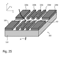
- Figure 25 shows a schematic perspective view of the apparatus 300 (dimensions are not to scale). It can be seen that parallel lines or bars 320a-320e of conductive graphene remain on the substrate 310. Each of these lines is cut into two pieces that may be connected to a circuit (not shown) and that lie on opposite sides of a (nano-) hole or aperture A3 through which single molecules M can pass. Moreover, each of the resulting electrode pairs 320a-320e may be put in its own microfluidic circuit (not shown).
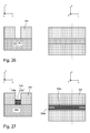
- FIGs 26-29 schematically illustrate a modification of the manufacturing procedure described above with respect to Figures 13-24 .
- the holes A3 through the substrate 310 are generated with the help of a self-assembling resist as the first step, not as the last.
- the procedure starts with the deposition of a primary resist 353 onto the substrate 310 (without graphene on top), which is considered as the processing layer PL1 for the next steps.
- the primary resist 353 has been patterned, e.g. by optical lithography, yielding a central trench in x-direction.
- Figure 27 shows that a self-assembling resist 358 has been deposited and self-assembled into a pattern of cylinders 358a of a first phase embedded in a second phase 358b.
- Figure 29 shows the device after a graphene layer 320 has been deposited on top of the substrate 310, covering the holes A3.
- the further manufacturing can now continue analogously to the steps of Figures 13-21 , according to which parallel stripes are first produced in the graphene layer (by slits A1) which are then cut perpendicularly in two (by a slit A2).
- the holes or apertures A3 in the substrate 310 are now already present, allowing to jump directly to the accomplished apparatus 300 of Figure 24 .
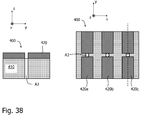
- FIGS 30-38 schematically illustrate consecutive steps of an alternative manufacturing procedure of an apparatus 400.
- This procedure starts in Figure 30 with the generation of (broad) stripes in a graphene layer 420 with the help of e.g. optical lithography.
- This graphene layer 420 is the "processing layer” PL1 for the next steps.
- a primary resist 451 has been deposited on the graphene layer 420 and already been patterned, for example by optical lithography, to yield a central trench perpendicular to the graphene stripes.
- Figure 32 shows the next step, in which a self-assembling resist 455 has been deposited in the aforementioned trench and has self-assembled into a pattern of three stripes of a first phase 455a and a second phase 455b extending in x-direction.
- Figure 38 shows the final apparatus 400 after the (optional) removal of the primary resist 452 and the remaining self-assembling resist 456b.
- the apparatus 400 has parallel lines or bars 420a-420c of conductive graphene, wherein each of these lines is cut into two pieces that may be connected to a circuit (not shown) and that lie on opposite sides of a (nano-) hole or aperture A3 through which single molecules M can pass.
- the device may be subject to further manufacturing steps, for example the application of additional (e.g. insulating) layers and/or the connection to a circuit (cf. Figures 1-4 ).
- each of the electrode pairs 4201-420c is put in its own microfluidic circuit.
- a procedure of the kind described above has been executed in an experiment.
- a silicon substrate was locally etched on the backside to a thickness of 100 nm or below.
- the substrate was provided with a graphene monolayer or bilayer.
- a resist was spincoated on the graphene layer and a trench of 100-300 nm was created in the resist layer.
- the trench was filled with a symmetrical block copolymer that formed a lamellar pattern upon annealing.
- the graphene layer may optionally be pre-treated with a neutral orientation layer, to achieve perpendicular alignment of the block copolymers.
- the lamellar block copolymer pattern was used as an etch resist mask to transfer the line spacer pattern in the graphene layer.
- a new trench with a trench width of approx. 30-60 nm was created by optical lithography perpendicular to the first trench.
- This trench was filled with an asymmetric block copolymer, capable of forming a cylindrical phase with perpendicular orientation of the cylinders with respect to the substrate and the cylinders being located on top of the thin graphene lines.
- the graphene layer may optionally be pre-treated with a neutral orientation layer, to achieve perpendicular alignment of the block copolymers (brush polymers may for example be used for this purpose, especially random brush copolymers consisting of randomly polymerized monomers A and B with an end group that can be reacted to surfaces).
- the block copolymer layer was used as an etch mask to etch through the graphene and through the underlying substrate. After stripping of the remaining block copolymer, an array of nanopores with thin graphene electrodes was obtained. Subsequently, the required contacts and the rest of the device could be made by conventional semiconductor-type process steps using Au electrodes with a 5 nm Cr under layer as contacts. Structuring these contact electrodes can be easily done with conventional lithography.
- the resist or another protective layer on top of the graphene (such as e.g. PMMA) is not removed or is given an optimal, for instance conical, shape.
- PMMA another protective layer on top of the graphene
- This increases the height of the slit on top of the graphene and thereby decreases the angle under which the ss-DNA will pass through the nano-opening in a crossed slit device.
- this has the crucial advantage that a very large shunt current through the ionic buffer solution on top of the graphene layer is avoided, which would overwhelm any small buffer current.
- the invention discloses the fabrication of nano-sequencing devices (solid state nanopores) using block co-polymer self-assembly, particularly of crossed-slit nano-sequencing devices.
- Said nano-sequencing devices may particularly be comprised of graphene layers.
Landscapes
- Engineering & Computer Science (AREA)
- Chemical & Material Sciences (AREA)
- Health & Medical Sciences (AREA)
- Physics & Mathematics (AREA)
- Life Sciences & Earth Sciences (AREA)
- Biomedical Technology (AREA)
- General Physics & Mathematics (AREA)
- Nanotechnology (AREA)
- Analytical Chemistry (AREA)
- Manufacturing & Machinery (AREA)
- Medicinal Chemistry (AREA)
- Biochemistry (AREA)
- Spectroscopy & Molecular Physics (AREA)
- Pathology (AREA)
- Immunology (AREA)
- General Health & Medical Sciences (AREA)
- Biophysics (AREA)
- Hematology (AREA)
- Molecular Biology (AREA)
- Urology & Nephrology (AREA)
- Food Science & Technology (AREA)
- Composite Materials (AREA)
- Microelectronics & Electronic Packaging (AREA)
- Condensed Matter Physics & Semiconductors (AREA)
- Materials Engineering (AREA)
- Crystallography & Structural Chemistry (AREA)
- Micromachines (AREA)
- Investigating Or Analyzing Materials By The Use Of Electric Means (AREA)
- Exposure And Positioning Against Photoresist Photosensitive Materials (AREA)
- Photosensitive Polymer And Photoresist Processing (AREA)
- Measuring Or Testing Involving Enzymes Or Micro-Organisms (AREA)
Priority Applications (5)
| Application Number | Priority Date | Filing Date | Title |
|---|---|---|---|
| US14/385,398 US9568464B2 (en) | 2012-03-22 | 2013-03-14 | Manufacturing method of an apparatus for the processing of single molecules |
| EP13720583.7A EP2828707B1 (fr) | 2012-03-22 | 2013-03-14 | Procédé de fabrication d'un appareil destiné au traitement de molécules individuelles. |
| PCT/IB2013/052026 WO2013140316A2 (fr) | 2012-03-22 | 2013-03-14 | Procédé de fabrication d'un appareil destiné au traitement de molécules individuelles. |
| CN201380026733.6A CN104350420B (zh) | 2012-03-22 | 2013-03-14 | 用于处理单分子的设备的制造方法 |
| JP2015501024A JP6322185B2 (ja) | 2012-03-22 | 2013-03-14 | 単一分子のプロセシングのための装置の製造方法 |
Applications Claiming Priority (1)
| Application Number | Priority Date | Filing Date | Title |
|---|---|---|---|
| US201261614051P | 2012-03-22 | 2012-03-22 |
Publications (1)
| Publication Number | Publication Date |
|---|---|
| EP2642341A2 true EP2642341A2 (fr) | 2013-09-25 |
Family
ID=45952890
Family Applications (2)
| Application Number | Title | Priority Date | Filing Date |
|---|---|---|---|
| EP12174261.3A Ceased EP2642341A2 (fr) | 2012-03-22 | 2012-06-29 | Méthode de fabrication d'un dispositif pour le traitement de molécules individuelles |
| EP13720583.7A Active EP2828707B1 (fr) | 2012-03-22 | 2013-03-14 | Procédé de fabrication d'un appareil destiné au traitement de molécules individuelles. |
Family Applications After (1)
| Application Number | Title | Priority Date | Filing Date |
|---|---|---|---|
| EP13720583.7A Active EP2828707B1 (fr) | 2012-03-22 | 2013-03-14 | Procédé de fabrication d'un appareil destiné au traitement de molécules individuelles. |
Country Status (5)
| Country | Link |
|---|---|
| US (1) | US9568464B2 (fr) |
| EP (2) | EP2642341A2 (fr) |
| JP (1) | JP6322185B2 (fr) |
| CN (1) | CN104350420B (fr) |
| WO (1) | WO2013140316A2 (fr) |
Cited By (1)
| Publication number | Priority date | Publication date | Assignee | Title |
|---|---|---|---|---|
| CN105531360A (zh) * | 2013-11-08 | 2016-04-27 | 株式会社日立高新技术 | Dna输送控制设备及其制造方法、以及dna测序装置 |
Families Citing this family (3)
| Publication number | Priority date | Publication date | Assignee | Title |
|---|---|---|---|---|
| KR101489154B1 (ko) * | 2014-06-26 | 2015-02-03 | 국민대학교산학협력단 | 잔류응력을 이용한 나노갭 센서의 제조방법 및 이에 의해 제조되는 나노갭 센서 |
| US10961563B1 (en) * | 2019-12-19 | 2021-03-30 | Robert Bosch Gmbh | Nanoscale topography system for use in DNA sequencing and method for fabrication thereof |
| CN111261586B (zh) * | 2020-01-22 | 2023-03-14 | 成都工业学院 | 一种中孔半导体纳米结构的制作方法 |
Citations (1)
| Publication number | Priority date | Publication date | Assignee | Title |
|---|---|---|---|---|
| US20100327847A1 (en) | 2007-09-12 | 2010-12-30 | President And Fellows Of Harvard College | High-Resolution Molecular Sensor |
Family Cites Families (20)
| Publication number | Priority date | Publication date | Assignee | Title |
|---|---|---|---|---|
| US7582490B2 (en) * | 1999-06-22 | 2009-09-01 | President And Fellows Of Harvard College | Controlled fabrication of gaps in electrically conducting structures |
| US20040124092A1 (en) * | 2002-12-30 | 2004-07-01 | Black Charles T. | Inorganic nanoporous membranes and methods to form same |
| EP1827717A4 (fr) * | 2004-11-22 | 2011-11-23 | Wisconsin Alumni Res Found | Procedes et compositions destines a la formation de films copolymeres a motif aperiodique |
| US8133534B2 (en) * | 2004-11-22 | 2012-03-13 | Wisconsin Alumni Research Foundation | Methods and compositions for forming patterns with isolated or discrete features using block copolymer materials |
| EP1721657A1 (fr) * | 2005-05-13 | 2006-11-15 | SONY DEUTSCHLAND GmbH | Méthode de fabrication d'une membrane polymère ayant au moins un pore |
| US7579278B2 (en) * | 2006-03-23 | 2009-08-25 | Micron Technology, Inc. | Topography directed patterning |
| US7553760B2 (en) * | 2006-10-19 | 2009-06-30 | International Business Machines Corporation | Sub-lithographic nano interconnect structures, and method for forming same |
| US8119017B2 (en) * | 2008-06-17 | 2012-02-21 | Hitachi Global Storage Technologies Netherlands B.V. | Method using block copolymers for making a master mold with high bit-aspect-ratio for nanoimprinting patterned magnetic recording disks |
| KR101535227B1 (ko) * | 2008-12-31 | 2015-07-08 | 삼성전자주식회사 | 블록 공중합체를 이용한 미세 패턴 형성 방법 |
| US8361704B2 (en) * | 2009-01-12 | 2013-01-29 | International Business Machines Corporation | Method for reducing tip-to-tip spacing between lines |
| US8398868B2 (en) * | 2009-05-19 | 2013-03-19 | International Business Machines Corporation | Directed self-assembly of block copolymers using segmented prepatterns |
| BR112012005888B1 (pt) * | 2009-09-18 | 2019-10-22 | President And Fellows Of Harvard College | sensores de nanoporo de grafeno e método para avaliar uma molécula de polímero |
| CN101694474B (zh) * | 2009-10-22 | 2012-10-10 | 浙江大学 | 一种纳米孔电学传感器 |
| US8821978B2 (en) * | 2009-12-18 | 2014-09-02 | International Business Machines Corporation | Methods of directed self-assembly and layered structures formed therefrom |
| US8206601B2 (en) * | 2009-12-18 | 2012-06-26 | Hitachi Global Storage Technologies Netherlands B.V. | Supporting membranes on nanometer-scale self-assembled films |
| US8828493B2 (en) * | 2009-12-18 | 2014-09-09 | International Business Machines Corporation | Methods of directed self-assembly and layered structures formed therefrom |
| US8623458B2 (en) * | 2009-12-18 | 2014-01-07 | International Business Machines Corporation | Methods of directed self-assembly, and layered structures formed therefrom |
| KR101432115B1 (ko) * | 2010-07-15 | 2014-08-21 | 한국전자통신연구원 | 메타 물질 및 그의 제조방법 |
| US8361321B2 (en) * | 2010-08-25 | 2013-01-29 | Lockheed Martin Corporation | Perforated graphene deionization or desalination |
| US8734904B2 (en) * | 2010-11-30 | 2014-05-27 | International Business Machines Corporation | Methods of forming topographical features using segregating polymer mixtures |
-
2012
- 2012-06-29 EP EP12174261.3A patent/EP2642341A2/fr not_active Ceased
-
2013
- 2013-03-14 EP EP13720583.7A patent/EP2828707B1/fr active Active
- 2013-03-14 US US14/385,398 patent/US9568464B2/en active Active
- 2013-03-14 WO PCT/IB2013/052026 patent/WO2013140316A2/fr not_active Ceased
- 2013-03-14 JP JP2015501024A patent/JP6322185B2/ja not_active Expired - Fee Related
- 2013-03-14 CN CN201380026733.6A patent/CN104350420B/zh not_active Expired - Fee Related
Patent Citations (1)
| Publication number | Priority date | Publication date | Assignee | Title |
|---|---|---|---|---|
| US20100327847A1 (en) | 2007-09-12 | 2010-12-30 | President And Fellows Of Harvard College | High-Resolution Molecular Sensor |
Non-Patent Citations (4)
| Title |
|---|
| BLACK ET AL., IBM J. RES. & DEV., vol. 51, no. 5, 2007, pages 605 |
| D. MALKO; C. NEISS; F. VINESC; A. GORLING, PHYS REV. LETT., vol. 108, 2012, pages 086804 |
| H.W.CH. POSTMA: "Rapid sequencing of individual DNA molecules in graphene nanogaps", NANO LETT., vol. 10, 2010, pages 420 - 425, XP055043958, DOI: doi:10.1021/nl9029237 |
| K.S. NOVOSELOV; A.K. GEIM; S.V. MOROZOV; D. JIANG; Y. ZHANG; S.V. DUBONOS; I.V. GRIGORIEVA; A.A. FIRSOV: "Electric Field Effect in Atomically Thin Carbon Films", SCIENCE, vol. 306, no. 204, pages 666 - 669, XP009086357, DOI: doi:10.1126/science.1102896 |
Cited By (2)
| Publication number | Priority date | Publication date | Assignee | Title |
|---|---|---|---|---|
| CN105531360A (zh) * | 2013-11-08 | 2016-04-27 | 株式会社日立高新技术 | Dna输送控制设备及其制造方法、以及dna测序装置 |
| CN105531360B (zh) * | 2013-11-08 | 2017-07-11 | 株式会社日立高新技术 | Dna输送控制设备及其制造方法、以及dna测序装置 |
Also Published As
| Publication number | Publication date |
|---|---|
| CN104350420A (zh) | 2015-02-11 |
| JP6322185B2 (ja) | 2018-05-09 |
| CN104350420B (zh) | 2018-11-20 |
| WO2013140316A2 (fr) | 2013-09-26 |
| US20150027980A1 (en) | 2015-01-29 |
| JP2015517097A (ja) | 2015-06-18 |
| EP2828707B1 (fr) | 2021-12-01 |
| WO2013140316A3 (fr) | 2014-01-23 |
| EP2828707A2 (fr) | 2015-01-28 |
| US9568464B2 (en) | 2017-02-14 |
Similar Documents
| Publication | Publication Date | Title |
|---|---|---|
| CN103890580B (zh) | 用于处理单分子的设备 | |
| US7781764B2 (en) | Nanometric device for the measurement of the conductivity and quantum effects of individual molecules and methods for the manufacture and use thereof | |
| US9881786B2 (en) | Methods of forming nanostructures using self-assembled nucleic acids, and nanostructures thereof | |
| JP6472208B2 (ja) | 核酸搬送制御デバイス及びその製造方法、並びに核酸シーケンシング装置 | |
| WO2018098286A1 (fr) | Dispositif de séquençage d'acide nucléique contenant du graphène | |
| EP2828707B1 (fr) | Procédé de fabrication d'un appareil destiné au traitement de molécules individuelles. | |
| CN108700542A (zh) | 裂纹结构、使用裂纹结构的隧穿结以及制作其的方法 | |
| CN101124089B (zh) | 纳米级电子光刻 | |
| US20140062454A1 (en) | Nanosensors including graphene and methods of manufacturing the same | |
| CN111108591B (zh) | 形成用于生物应用的自支撑膜的方法 | |
| JP2012015497A (ja) | 交差した導電あるいは半導電アクセス・ラインのクロスバー・アレイの実現方法 | |
| KR20220115961A (ko) | Dna 시퀀싱에 사용하기 위한 나노스케일 토포그래피 시스템 및 이의 제조 방법 | |
| US20130082722A1 (en) | Method of forming nanopore and structure formed with nanopore | |
| Wu et al. | Fabrication of compact collateral silicon nanowires based on continuously alternating deposition |
Legal Events
| Date | Code | Title | Description |
|---|---|---|---|
| PUAI | Public reference made under article 153(3) epc to a published international application that has entered the european phase |
Free format text: ORIGINAL CODE: 0009012 |
|
| AK | Designated contracting states |
Kind code of ref document: A2 Designated state(s): AL AT BE BG CH CY CZ DE DK EE ES FI FR GB GR HR HU IE IS IT LI LT LU LV MC MK MT NL NO PL PT RO RS SE SI SK SM TR |
|
| AX | Request for extension of the european patent |
Extension state: BA ME |
|
| STAA | Information on the status of an ep patent application or granted ep patent |
Free format text: STATUS: THE APPLICATION HAS BEEN REFUSED |
|
| 18R | Application refused |
Effective date: 20130317 |