EP2642537A2 - Lichtemittierende Vorrichtung und Verfahren zu ihrer Herstellung - Google Patents
Lichtemittierende Vorrichtung und Verfahren zu ihrer Herstellung Download PDFInfo
- Publication number
- EP2642537A2 EP2642537A2 EP13156535.0A EP13156535A EP2642537A2 EP 2642537 A2 EP2642537 A2 EP 2642537A2 EP 13156535 A EP13156535 A EP 13156535A EP 2642537 A2 EP2642537 A2 EP 2642537A2
- Authority
- EP
- European Patent Office
- Prior art keywords
- section
- light emitting
- translucent
- distribution control
- light distribution
- Prior art date
- Legal status (The legal status is an assumption and is not a legal conclusion. Google has not performed a legal analysis and makes no representation as to the accuracy of the status listed.)
- Withdrawn
Links
Images





Classifications
-
- H—ELECTRICITY
- H10—SEMICONDUCTOR DEVICES; ELECTRIC SOLID-STATE DEVICES NOT OTHERWISE PROVIDED FOR
- H10H—INORGANIC LIGHT-EMITTING SEMICONDUCTOR DEVICES HAVING POTENTIAL BARRIERS
- H10H20/00—Individual inorganic light-emitting semiconductor devices having potential barriers, e.g. light-emitting diodes [LED]
- H10H20/80—Constructional details
- H10H20/85—Packages
- H10H20/855—Optical field-shaping means, e.g. lenses
-
- H—ELECTRICITY
- H10—SEMICONDUCTOR DEVICES; ELECTRIC SOLID-STATE DEVICES NOT OTHERWISE PROVIDED FOR
- H10H—INORGANIC LIGHT-EMITTING SEMICONDUCTOR DEVICES HAVING POTENTIAL BARRIERS
- H10H20/00—Individual inorganic light-emitting semiconductor devices having potential barriers, e.g. light-emitting diodes [LED]
- H10H20/01—Manufacture or treatment
-
- H—ELECTRICITY
- H10—SEMICONDUCTOR DEVICES; ELECTRIC SOLID-STATE DEVICES NOT OTHERWISE PROVIDED FOR
- H10H—INORGANIC LIGHT-EMITTING SEMICONDUCTOR DEVICES HAVING POTENTIAL BARRIERS
- H10H20/00—Individual inorganic light-emitting semiconductor devices having potential barriers, e.g. light-emitting diodes [LED]
- H10H20/80—Constructional details
- H10H20/81—Bodies
- H10H20/819—Bodies characterised by their shape, e.g. curved or truncated substrates
- H10H20/82—Roughened surfaces, e.g. at the interface between epitaxial layers
-
- H—ELECTRICITY
- H10—SEMICONDUCTOR DEVICES; ELECTRIC SOLID-STATE DEVICES NOT OTHERWISE PROVIDED FOR
- H10H—INORGANIC LIGHT-EMITTING SEMICONDUCTOR DEVICES HAVING POTENTIAL BARRIERS
- H10H20/00—Individual inorganic light-emitting semiconductor devices having potential barriers, e.g. light-emitting diodes [LED]
- H10H20/01—Manufacture or treatment
- H10H20/036—Manufacture or treatment of packages
- H10H20/0363—Manufacture or treatment of packages of optical field-shaping means
-
- H—ELECTRICITY
- H10—SEMICONDUCTOR DEVICES; ELECTRIC SOLID-STATE DEVICES NOT OTHERWISE PROVIDED FOR
- H10H—INORGANIC LIGHT-EMITTING SEMICONDUCTOR DEVICES HAVING POTENTIAL BARRIERS
- H10H20/00—Individual inorganic light-emitting semiconductor devices having potential barriers, e.g. light-emitting diodes [LED]
- H10H20/80—Constructional details
- H10H20/85—Packages
- H10H20/8506—Containers
-
- H—ELECTRICITY
- H10—SEMICONDUCTOR DEVICES; ELECTRIC SOLID-STATE DEVICES NOT OTHERWISE PROVIDED FOR
- H10H—INORGANIC LIGHT-EMITTING SEMICONDUCTOR DEVICES HAVING POTENTIAL BARRIERS
- H10H20/00—Individual inorganic light-emitting semiconductor devices having potential barriers, e.g. light-emitting diodes [LED]
- H10H20/80—Constructional details
- H10H20/85—Packages
- H10H20/851—Wavelength conversion means
-
- H—ELECTRICITY
- H10—SEMICONDUCTOR DEVICES; ELECTRIC SOLID-STATE DEVICES NOT OTHERWISE PROVIDED FOR
- H10H—INORGANIC LIGHT-EMITTING SEMICONDUCTOR DEVICES HAVING POTENTIAL BARRIERS
- H10H20/00—Individual inorganic light-emitting semiconductor devices having potential barriers, e.g. light-emitting diodes [LED]
- H10H20/80—Constructional details
- H10H20/85—Packages
- H10H20/851—Wavelength conversion means
- H10H20/8514—Wavelength conversion means characterised by their shape, e.g. plate or foil
-
- H—ELECTRICITY
- H10—SEMICONDUCTOR DEVICES; ELECTRIC SOLID-STATE DEVICES NOT OTHERWISE PROVIDED FOR
- H10H—INORGANIC LIGHT-EMITTING SEMICONDUCTOR DEVICES HAVING POTENTIAL BARRIERS
- H10H20/00—Individual inorganic light-emitting semiconductor devices having potential barriers, e.g. light-emitting diodes [LED]
- H10H20/80—Constructional details
- H10H20/85—Packages
- H10H20/855—Optical field-shaping means, e.g. lenses
- H10H20/856—Reflecting means
-
- H—ELECTRICITY
- H10—SEMICONDUCTOR DEVICES; ELECTRIC SOLID-STATE DEVICES NOT OTHERWISE PROVIDED FOR
- H10H—INORGANIC LIGHT-EMITTING SEMICONDUCTOR DEVICES HAVING POTENTIAL BARRIERS
- H10H20/00—Individual inorganic light-emitting semiconductor devices having potential barriers, e.g. light-emitting diodes [LED]
- H10H20/80—Constructional details
- H10H20/85—Packages
- H10H20/857—Interconnections, e.g. lead-frames, bond wires or solder balls
Definitions
- a light emitting device including a chip-like semiconductor light emitting element (hereinafter simply referred to as light emitting element).
- Such a light emitting device In such a light emitting device, light emitted from the light emitting element is emitted toward a wide range on the front side of the light emitting device. Thus, the emission intensity of the light emitting device has a wide light distribution characteristic.
- a light emitting device has been used in various applications such as the light source of an illumination device, the backlight source of an image display device, and the light source of a display device.
- the light emitting device having a wide light distribution characteristic may emit wasted light in some applications.
- a light emitting device in general, includes a light emitting element, a translucent section, and a light distribution control section.
- the light emitting element includes a first surface.
- the first surface emits light.
- the translucent section is provided on the first surface.
- the light distribution control section is provided on a periphery of the first surface.
- the light distribution control section has a lower refractive index than the translucent section.
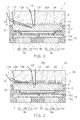
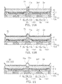
- FIG. 1 is a schematic sectional view illustrating a light emitting device according to a first embodiment.
- the light emitting device 1 includes a light emitting element 2, a translucent section 6, an insulating section 7, a first electrode section 8a, a second electrode section 8b, a sealing section 12, and a light distribution control section 13.
- the light emitting element 2 can be e.g. a light emitting diode.
- the light emitting element 2 includes e.g. a first semiconductor layer 3, a light emitting layer 4 provided on the first semiconductor layer 3, and a second semiconductor layer 5 provided on the light emitting layer 4.
- the first semiconductor layer 3 is a layer formed from e.g. a semiconductor doped into p-type (p-type semiconductor).
- the light emitting layer 4 has e.g. a quantum well structure composed of a well layer in which holes and electrons are recombined to generate light, and a barrier layer having a larger band gap than the well layer.
- the second semiconductor layer 5 is a layer formed from e.g. a semiconductor doped into n-type (n-type semiconductor).
- the semiconductor is e.g. a nitride semiconductor.
- the nitride semiconductor is e.g. GaN (gallium nitride), AlN (aluminum nitride), AlGaN (aluminum gallium nitride), or InGaN (indium gallium nitride).
- the light emitting surface 2a (corresponding to an example of the first surface) of the light emitting element 2 is provided with an uneven portion 2a1.
- the uneven portion 2a1 suppresses the total reflection of the light emitted from the light emitting element 2. This can increase the efficiency of extracting the light generated in the light emitting element 2.
- the translucent section 6 is provided on the surface 2a of the light emitting element 2.
- the translucent section 6 is formed from a translucent material.
- the translucent material is e.g. a translucent resin.
- the translucent resin is e.g. epoxy resin, silicone resin, methacrylate resin (PMMA), polycarbonate (PC), cyclic polyolefin (COP), alicyclic acrylate (OZ), allyl diglycol carbonate (ADC), acrylate resin, fluororesin, hybrid resin of silicone resin and epoxy resin, or urethane resin.
- the insulating section 7 is provided so as to cover the surface 2b on the opposite side from the light emitting side of the light emitting element 2.
- the insulating section 7 can be formed from e.g. SiO 2 (silicon oxide).
- the first electrode section 8a includes e.g. a first seed section 9a, a first wiring section 10a, and a first pillar section 11a.
- the second electrode section 8b includes e.g. a second seed section 9b, a second wiring section 10b, and a second pillar section 11b.
- An electrode, not shown, provided on the surface of the first semiconductor layer 3 is connected to the first pillar section 11a via the first seed section 9a and the first wiring section 10a.
- An electrode, not shown, provided on the surface of the second semiconductor layer 5 is connected to the second pillar section 11b via the second seed section 9b and the second wiring section 10b.
- the first electrode section 8a is an extraction electrode connected to the electrode, not shown, provided on the first semiconductor layer 3.
- the second electrode section 8b is an extraction electrode connected to the electrode, not shown, provided on the second semiconductor layer 5.
- the first seed section 9a, the first wiring section 10a, the first pillar section 11a, the second seed section 9b, the second wiring section 10b, and the second pillar section 11b can be formed from e.g. a metal such as copper, gold, nickel, and silver. In this case, in view of e.g. thermal conductivity, migration resistance, and adhesiveness to the sealing section 12, these sections are preferably formed from copper.
- the sealing section 12 includes a first sealing section 12a and a second sealing section 12b.
- the first sealing section 12a is provided so as to cover the surface 2b side and the side surface 2c (corresponding to an example of the second surface) side of the light emitting element 2.
- the second sealing section 12b is provided so as to cover the first wiring section 10a, the first pillar section 11a, the second wiring section 10b, and the second pillar section 11b. However, the end surface 11a1 of the first pillar section 11a and the end surface 11b1 of the second pillar section 11b are exposed from the second sealing section 12b.
- the first sealing section 12a and the second sealing section 12b can be formed from an organic material or inorganic material having insulating property.
- the first sealing section 12a, the second sealing section 12b, and the insulating section 7 can be integrally formed.
- the thickness of the first pillar section 11a, the second pillar section 11b, and the second sealing section 12b can be thickened. Then, even if the thickness of the light emitting element 2 is thin, the decrease of mechanical strength of the light emitting element 2 can be compensated.
- the light distribution control section 13 is provided on the periphery of the surface 2a of the light emitting element 2.
- the light distribution control section 13 can be provided so as to surround the surface 2a of the light emitting element 2.
- the light distribution control section 13 can be provided on part of the periphery of the surface 2a.
- the light distribution control section 13 can be provided so as to partly extend to the inside of the outline of the surface 2a.
- the light distribution control section 13 can be provided outside the outline of the surface 2a, or can be provided so that the outline of the light distribution control section 13 overlaps the outline of the surface 2a.
- the refractive index of the light distribution control section 13 is lower than the refractive index of the translucent section 6.
- the light L1 incident on the light distribution control section 13 is refracted toward the front side of the light emitting device 1.
- the material of the light distribution control section 13 is not particularly limited, but can be appropriately selected from inorganic materials and organic materials such that the refractive index of the light distribution control section 13 is lower than the refractive index of the translucent section 6.
- the light distribution control section 13 can be translucent.
- the light distribution control section 13 can be formed from a translucent material such as transparent and semi-transparent material.
- the light distribution control section 13 can be formed from a material having high reflectance such as white resin.
- the light distribution control section 13 includes an inclined surface 13a inclined in a direction such that the tip of the light distribution control section 13 is located away from the center side of the surface 2a.
- the translucent section 6 is provided so as to cover the inclined surface 13a.
- the light distribution control section 13 including the inclined surface 13a can increase the incident angle of the light L2 incident on the light distribution control section 13. This facilitates total reflection of the light L2, and hence facilitates emitting the light L2 toward the front side of the light emitting device 1.
- the inclined surface 13a is a curved surface.
- the inclined surface 13a may be a flat surface.
- the height dimension H of the light distribution control section 13 is not particularly limited. However, a larger height dimension H of the light distribution control section 13 facilitates emitting the light toward the front side of the light emitting device 1. The details on the height dimension H of the light distribution control section 13 will be described later (see, e.g., FIGS. 4A and 4B ).
- the light L3 and the light L4 emitted from the light emitting element 2 toward the front side of the light emitting device 1 are emitted toward the front side of the light emitting device 1 without being incident on the light distribution control section 13.
- a light distribution control section 13 having a lower refractive index than the translucent section 6 is provided. This can increase the light emitted to the front side of the light emitting device 1. That is, because the light distribution control section 13 having a lower refractive index than the translucent section 6 is provided, the light distribution characteristic can be narrowed.
- a desired light distribution characteristic can be obtained by changing the refractive index of the light distribution control section 13, the angle of the inclined surface 13a, and the height dimension H of the light distribution control section 13.
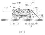
- FIG. 2 is a schematic sectional view illustrating a light emitting device according to a second embodiment.
- the light emitting device 21 includes a light emitting element 2, a translucent section 26, an insulating section 7, a first electrode section 8a, a second electrode section 8b, a sealing section 12, and a light distribution control section 13.
- the translucent section 26 is provided on the surface 2a of the light emitting element 2.
- the translucent section 26 includes a translucent material and a phosphor 26a.
- the translucent material can be made similar to that of the translucent section 6 described above.
- the refractive index of the light distribution control section 13 is lower than the refractive index of the translucent section 26.
- the phosphor 26a is unevenly distributed inside the translucent section 26 on the surface 2a side of the light emitting element 2. That is, the phosphor 26a is provided inside the translucent section 26 near the surface 2a of the light emitting element 2.
- the phosphor 26a can be in contact with the surface 2a of the light emitting element 2.
- the phosphor 26a is located only inside the periphery of the surface 2a of the light emitting element 2.
- the phosphor 26a is particulate.
- the phosphor 26a absorbs part of the light emitted from the light emitting element 2 and emits fluorescence having a prescribed wavelength.
- the phosphor 26a can absorb part of blue light emitted from the light emitting element 2 and emit yellow fluorescence.
- blue light L3, L4 not absorbed by the phosphor 26a and yellow fluorescence L1a, L2a emitted from the phosphor 26a are emitted from the translucent section 26.
- blue light emitted from the light emitting element 2 it is possible to use only a phosphor emitting yellow fluorescence.
- blue light emitted from the light emitting element 2 it is also possible to use a phosphor emitting red fluorescence and a phosphor emitting green fluorescence in combination. In this case, blue light, red light, and green light are emitted from the translucent section 26.
- Examples of the material of the phosphor emitting yellow fluorescence can include the following. However, the phosphor emitting yellow fluorescence is not limited thereto, but can be appropriately modified.
- Examples of the material of the phosphor emitting red fluorescence can include the following. However, the phosphor emitting red fluorescence is not limited thereto, but can be appropriately modified.
- Examples of the material of the phosphor emitting green fluorescence can include the following. However, the phosphor emitting green fluorescence is not limited thereto, but can be appropriately modified.
- the kind and combination of the colors of fluorescence emitted by the phosphor are not limited to those illustrated, but can be appropriately modified depending on the purpose and the like of the light emitting device 21.
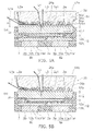
- FIG. 3 is a schematic sectional view illustrating a light emitting device according to a comparative example.
- FIG. 3 shows the light emitting device 121 according to the comparative example mounted on a substrate 122.
- the bonding section 123 in FIG. 3 is formed from e.g. solder.
- a phosphor 126a is dispersed inside the translucent section 126.
- the transmission length of the light transmitted inside the translucent section 126 is varied with the direction of the light emitted from the light emitting element 2.
- the amount of phosphor contained in the transmission length is varied with the direction of the light emitted from the light emitting element 2.
- the amount of phosphor 126a contained in the transmission length is increased. This increases the amount of fluorescence emitted from the phosphor 126a.
- the tint is varied with the direction of the light emitted from the light emitting element 2.
- the phosphor 26a is unevenly distributed inside the translucent section 26 on the surface 2a side of the light emitting element 2.
- the variation of the amount of the phosphor 26a contained in the transmission length can be suppressed.
- the variation of the tint with the direction of the light emitted from the light emitting element 2 can be suppressed.
- the phosphor 126a is dispersed inside the translucent section 126.
- the fluorescence L101 emitted from the phosphor 126a is emitted in a wide range on the front side and side surface side of the light emitting device 121.
- the fluorescence L102 emitted from the phosphor 126a is emitted toward the substrate 122 on the rear side of the light emitting device 121.
- the fluorescence L102 emitted toward the substrate 122 is reflected by the substrate 122, but incurs a greater loss.
- the light emitting device 121 has a wide light distribution characteristic. However, this may be unsuitable depending on the purpose of the light emitting device 121.
- the refractive index of the light distribution control section 13 is lower than the refractive index of the translucent section 26. This can increase the light emitted to the front side of the light emitting device 21. That is, because the light distribution control section 13 having a lower refractive index than the translucent section 26 is provided, the light distribution characteristic can be narrowed.
- a desired light distribution characteristic can be obtained by changing the refractive index of the light distribution control section 13, the angle of the inclined surface 13a, and the height dimension H of the light distribution control section 13.
- the height dimension of the light distribution control section 13 is now further illustrated.
- FIGS. 4A and 4B are schematic sectional views illustrating the height dimension of the light distribution control section 13.
- the fluorescence L2a1 emitted from the phosphor 26a is made more likely to be emitted from the side surface side of the light emitting device 21a without being incident on the light distribution control section 13.
- the light distribution characteristic can be widened.
- the height dimension Ha of the light distribution control section 13 can be made larger than e.g. the average diameter dimension of the phosphor 26a.
- the fluorescence L2a emitted from the phosphor 26a is made more likely to be incident on the light distribution control section 13. This facilitates emitting the light from the front side of the light emitting device 21.
- the light distribution characteristic can be narrowed.
- the height dimension Hb of the light distribution control section 13 can be made less than or equal to the thickness dimension of the translucent section 26.
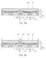
- FIGS. 5A and 5B are schematic sectional views illustrating light emitting devices according to a third embodiment.
- the light emitting device 51a includes a light emitting element 2, a translucent section 26, an insulating section 7, a first electrode section 8a, a second electrode section 8b, a sealing section 12, a light distribution control section 53a, and a translucent film 54.
- the translucent film 54 includes a film section 54a and a protrusion 54b.
- the film section 54a is provided so as to cover the surface 2a of the light emitting element 2.
- the protrusion 54b is provided on the periphery of the surface 2a of the light emitting element 2.
- the protrusion 54b protrudes in a direction away from the surface 2a.
- a space is provided on the inner surface 54b1 side of the protrusion 54b. That is, a space is provided on the periphery of the surface 2a of the light emitting element 2.
- the space provided on the periphery of the surface 2a is filled with the gas in the atmosphere in which the light emitting device 51a is provided.
- the gas in the atmosphere in which the light emitting device 51a is provided is e.g. air.
- the refractive index of the gas in the atmosphere in which the light emitting device 51a is provided is lower than the refractive index of the material forming the translucent section 26.
- the space provided on the periphery of the surface 2a can be used as the light distribution control section 53a.
- the translucent film 54 is provided between the inclined surface of the light distribution control section 53a and the translucent section 26.
- the light distribution control section 13 illustrated in FIGS. 1 and 2 includes an inorganic material or organic material.
- the light distribution control section 53a includes the gas in the atmosphere in which the light emitting device 51a is provided.
- the translucent film 54 can be formed from a translucent material.
- the translucent film 54 can be formed from e.g. SiO 2 or SiN (silicon nitride).
- the refractive index of the translucent film 54 is not particularly limited. However, the refractive index of the translucent film 54 is preferably made lower than the refractive index of the translucent section 26.
- the translucent film 54 is not necessarily needed, but can be omitted. However, providing the translucent film 54 facilitates forming the light distribution control section 53a.
- the light emitting device 51b includes a light emitting element 2, a translucent section 26, an insulating section 7, a first electrode section 8a, a second electrode section 8b, a sealing section 12, and a light distribution control section 53b.
- a recess 26b is provided on the side surface of the translucent section 26.
- the recess 26b is provided on the periphery of the surface 2a of the light emitting element 2. That is, by providing the recess 26b, a space is provided on the periphery of the surface 2a of the light emitting element 2.
- the space provided on the periphery of the surface 2a is filled with the gas in the atmosphere in which the light emitting device 51b is provided.
- the gas in the atmosphere in which the light emitting device 51b is provided is e.g. air.
- the space provided on the periphery of the surface 2a can be used as the light distribution control section 53b.
- the light distribution control section 53b includes the gas in the atmosphere in which the light emitting device 51b is provided.
- the light distribution control section 53a illustrated in FIG. 5A is composed of the space provided on the inner surface 54b1 side of the protrusion 54b.
- the light distribution control section 53b is composed of the space provided on the side surface side of the translucent section 26. That is, the light distribution control section 53b corresponds to the case where the translucent film 54 described above is not provided.
- the light emitting devices 51a and 51b according to this embodiment can also achieve a function and effect similar to those of the light emitting device 21 described above.
- FIG. 6 is a schematic sectional view illustrating a light emitting device according to a fourth embodiment.
- the light emitting device 61 includes a light emitting element 2, a translucent section 26, an insulating section 7, a first electrode section 8a, a second electrode section 8b, a sealing section 12, a light distribution control section 63, a protective film 64, and a reflecting section 65.
- the light distribution control section 63 can be made similar to the light distribution control section 53b described above. That is, the space formed by providing a recess 26b on the side surface of the translucent section 26 constitutes the light distribution control section 63.
- the protective film 64 is provided so as to cover the surface 2a of the light emitting element 2.
- the protective film 64 can be formed from a translucent material.
- the protective film 64 can be formed from e.g. SiO 2 .
- the reflecting section 65 is provided on the side surface 2c side of the light emitting element 2.
- the reflecting section 65 can be formed from a material having high reflectance.
- the material having high reflectance is e.g. metal.
- the reflecting section 65 is preferably formed from e.g. aluminum.
- the light distribution control section 63 is composed of the space provided on the side surface side of the translucent section 26, the light incident on the light distribution control section 63 is made more likely to be emitted to the side surface side of the light emitting device 61.
- the reflecting section 65 is provided on the side surface 2c side of the light emitting element 2. Thus, the light L5 directed to the side surface side of the light emitting device 61 can be reflected.
- the light distribution characteristic can be changed by changing the height dimension of the reflecting section 65.
- the light emitting device 61 according to this embodiment can also achieve a function and effect similar to those of the light emitting device 21 described above.
- the light emitting devices illustrated above correspond to the case of the light emitting device based on WLP (wafer-level package).
- the embodiments are not limited to the light emitting device based on WLP, but are widely applicable to a light emitting device in which a translucent section is provided on the light emitting surface 2a of the light emitting element 2.
- the embodiments are also applicable to a light emitting device in which the light emitting element 2 is flip-chip connected to a substrate including a wiring layer.
- FIGS. 7A to 7C are schematic process sectional views illustrating the steps from forming a light emitting element 2 to forming a sealing section 12 in the method for manufacturing a light emitting device.
- a second semiconductor layer 5 on the surface 70a of a substrate 70 made of e.g. sapphire, a second semiconductor layer 5, a light emitting layer 4, and a first semiconductor layer 3 are formed. That is, a light emitting element 2 including a light emitting surface 2a is formed. Then, an insulating section 7 is formed on the surface of the second semiconductor layer 5 and the first semiconductor layer 3. A first seed section 9a is formed on the surface of the first semiconductor layer 3. A second seed section 9b is formed on the surface of the second semiconductor layer 5.
- These components can be formed by known techniques such as film formation, photolithography, and dry etching.
- a first sealing section 12a is formed on the entire surface on the surface 70a side.
- An opening 12a1 is formed so as to expose part of the first seed section 9a and the second seed section 9b.
- a film constituting a first wiring section 10a, a second wiring section 10b, a first pillar section 11a, and a second pillar section 11b is formed.
- a first wiring section 10a, a second wiring section 10b, a first pillar section 11a, and a second pillar section 11b are successively formed.
- a film constituting a second sealing section 12b is formed on the entire surface on the surface 70a side. The film is planarized so as to expose the end surface 11a1 of the first pillar section 11a and the end surface 11b1 of the second pillar section 11b.
- a second sealing section 12b is formed.
- the substrate 70 is removed.
- FIGS. 8A and 8B are schematic process sectional views illustrating the steps from forming an uneven portion 2a1 to forming a light distribution control section 13 in the method for manufacturing a light emitting device.
- an uneven portion 2a1 is formed on the surface 2a of the light emitting element 2.
- the uneven portion 2a1 can be formed by using the wet etching technique.
- the surface 2a can be wet etched with an aqueous solution of tetramethylammonium hydroxide ((CH 3 ) 4 NOH) (TMH) or an aqueous solution of potassium hydroxide (KOH) to form an uneven portion 2a1 based on the crystal structure.
- THF tetramethylammonium hydroxide
- KOH potassium hydroxide
- an uneven portion 2a1 can be formed on the surface 2a by using the photolithography technique and dry etching technique.
- a light distribution control section 13 is formed on the periphery of the surface 2a.
- a light distribution control section 13 having a lower refractive index than the translucent section 6, 26 is formed.
- the light distribution control section 13 can be formed by using a technique such as vacuum screen printing and molding.
- a resin having a prescribed refractive index is applied to the periphery of the surface 2a of the light emitting element 2, and cured to form a light distribution control section 13.
- a resin having a prescribed refractive index is applied to the periphery of the surface 2a of the light emitting element 2, and cured to form a light distribution control section 13.
- the side surface of the applied resin can be shaped into an inclined surface.
- a light distribution control section 13 including an inclined surface 13a can be formed.
- FIGS. 9A and 9B are schematic process sectional views illustrating the step of forming a translucent section 6, 26 in the method for manufacturing a light emitting device.
- a translucent section 6 is formed so as to cover the entire surface on the surface 2a side of the light emitting element 2.
- the translucent section 6 can be formed by using a technique such as vacuum screen printing and molding.
- a translucent resin is applied to the surface 2a side of the light emitting element 2, and cured to form a translucent section 6.
- a translucent section 26 including a phosphor 26a is formed so as to cover the entire surface on the surface 2a side of the light emitting element 2.
- the translucent section 26 can be formed by using a technique such as vacuum screen printing and molding.
- a translucent resin including a phosphor 26a is applied to the surface 2a side of the light emitting element 2, and cured to form a translucent section 26.
- the phosphor 26a After applying a resin including a phosphor 26a, the phosphor 26a can be sedimented in the resin so that the phosphor 26a is unevenly distributed on the surface 2a side of the light emitting element 2.
- a phosphor 26a can be added and sedimented in the resin.
- the sedimentation can be caused by gravity.
- the viscosity of the resin By adjusting the viscosity of the resin, sedimentation of the phosphor 26a can be facilitated.
- the viscosity of the resin can be adjusted by e.g. changing the amount of filler added to the resin or changing the amount of solvent added to the resin.
- FIGS. 10A, 10B, and 11 are schematic process sectional views illustrating the step of forming a light distribution control section 53a in the method for manufacturing a light emitting device.
- a sacrificial layer 71 is formed on the periphery of the surface 2a of the light emitting element 2.
- a technique such as vacuum screen printing and molding
- an inclined surface 71a can be formed on the sacrificial layer 71.
- the sacrificial layer 71 can be formed by applying a resist using a technique such as vacuum screen printing and molding.
- a film 72 constituting a translucent film 54 is formed so as to cover the entire surface on the surface 2a side of the light emitting element 2.
- a film 72 constituting a translucent film 54 is formed so as to cover the sacrificial layer 71.
- the film 72 constituting a translucent film 54 can be formed by forming a film made of SiO 2 or SiN using a technique such as sputtering.
- a hole 72a reaching e.g. the top of the sacrificial layer 71 is formed in the film 72.
- the sacrificial layer 71 is removed via the hole 72a.
- a translucent film 54 including a film section 54a and a protrusion 54b is formed.
- the space formed by removing the sacrificial layer 71 constitutes a light distribution control section 53a.
- the sacrificial layer 71 can be removed by a technique such as wet etching with e.g. acetone, and dry etching with e.g. oxygen plasma.
- the light distribution control section 53b can be formed as follows.
- a sacrificial layer 71 is formed on the periphery of the surface 2a of the light emitting element 2.
- a translucent section 6, 26 is formed so as to cover the sacrificial layer 71.
- a hole reaching e.g. the top of the sacrificial layer 71 is formed in the translucent section 6, 26. The sacrificial layer 71 is removed via the hole.
- the translucent section 6, 26 described above can be formed.
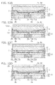
- FIGS. 12A to 12D are schematic process sectional views illustrating the steps of forming a protective film 64 and a reflecting section 65.
- a protective film 64 is formed so as to cover the entire surface on the surface 2a side of the light emitting element 2. For instance, by using the spin coating technique, a SOG (spin on glass) film is formed. Thus, a protective film 64 is formed. The protective film 64 is provided to protect the surface 2a of the light emitting element 2 in forming a reflecting section 65.
- SOG spin on glass
- the protective film 64 located on the side surface side of the second semiconductor layer 5 is removed. Furthermore, the upper surface 12a2 of the first sealing section 12a located on the side surface side of the second semiconductor layer 5 is set back. Here, the position of the upper surface 12a2 can be set above the lower surface 5a of the second semiconductor layer 5.
- the removal of the protective film 64 and the setting back of the upper surface 12a2 of the first sealing section 12a can be performed by using e.g. the photolithography technique and dry etching technique.
- a film 73 constituting a reflecting section 65 is formed so as to cover the entire surface on the surface 2a side of the light emitting element 2.
- the film 73 constituting a reflecting section 65 can be formed by forming a film made of aluminum using a technique such as sputtering.
- the film 73 other than the portion located on the side surface side of the second semiconductor layer 5 is removed to form a reflecting section 65.
- the reflecting section 65 can be formed by using e.g. the photolithography technique and an anisotropic etching technique such as the RIE (reactive ion etching) technique.
- the RIE technique using a chlorine-containing gas can be used.
- the thickness of the protective film 64 by changing the thickness of the protective film 64, the height dimension of the reflecting section 65 can be changed.
- the light distribution characteristic can be changed.
- the formation of the light distribution control section 13, 53a, 53b and the formation of the translucent section 6, 26 described above can be performed.
- a plurality of light emitting devices can be collectively manufactured.
- the light emitting devices are singulated.
- FIGS. 13A to 13C are schematic process sectional views illustrating the singulation of the light emitting device.
- FIG. 13A illustrates the singulation of the light emitting device 21.
- FIG. 13B illustrates the singulation of the light emitting device 51a.
- FIG. 13C illustrates the singulation of the light emitting device 61.
- the light emitting devices are singulated.
- Examples of the cutting method can include mechanical cutting using e.g. a diamond blade, cutting based on laser irradiation, and cutting with high-pressure water.
- the manufacturing method as described above can efficiently manufacture a light emitting device capable of changing the light distribution characteristic.
- a light emitting device as small as the size of the light emitting element 2 can be easily manufactured.
- mounting members such as a lead frame and ceramic substrate.
- wiring, sealing and the like can be performed on the wafer level.
- inspection can be performed on the wafer level.
- the productivity of the manufacturing process can be improved. As a result, cost reduction is facilitated.
- the embodiments illustrated above can realize a light emitting device capable of changing the light distribution characteristic and a method for manufacturing the same.
Landscapes
- Led Device Packages (AREA)
Applications Claiming Priority (1)
| Application Number | Priority Date | Filing Date | Title |
|---|---|---|---|
| JP2012062816A JP2013197309A (ja) | 2012-03-19 | 2012-03-19 | 発光装置 |
Publications (2)
| Publication Number | Publication Date |
|---|---|
| EP2642537A2 true EP2642537A2 (de) | 2013-09-25 |
| EP2642537A3 EP2642537A3 (de) | 2014-01-01 |
Family
ID=47749695
Family Applications (1)
| Application Number | Title | Priority Date | Filing Date |
|---|---|---|---|
| EP13156535.0A Withdrawn EP2642537A3 (de) | 2012-03-19 | 2013-02-25 | Lichtemittierende Vorrichtung und Verfahren zu ihrer Herstellung |
Country Status (4)
| Country | Link |
|---|---|
| US (1) | US9076937B2 (de) |
| EP (1) | EP2642537A3 (de) |
| JP (1) | JP2013197309A (de) |
| TW (1) | TW201349596A (de) |
Cited By (16)
| Publication number | Priority date | Publication date | Assignee | Title |
|---|---|---|---|---|
| EP2866271A1 (de) * | 2013-10-28 | 2015-04-29 | Kabushiki Kaisha Toshiba | Lichtemittierendes Halbleiterbauelement |
| EP3098861A1 (de) * | 2015-05-29 | 2016-11-30 | Nichia Corporation | Lichtemittierende vorrichtung, verfahren zur herstellung eines abdeckungselements und verfahren zur herstellung einer lichtemittierenden vorrichtung |
| EP3327800A1 (de) * | 2016-11-25 | 2018-05-30 | Seoul Viosys Co. Ltd. | Leuchtdiode mit lichtblockierungsschicht |
| WO2020229576A3 (de) * | 2019-05-14 | 2021-01-07 | Osram Opto Semiconductors Gmbh | Beleuchtungseinheit, verfahren zur herstellung einer beleuchtungseinheit, konverterelement für ein opto-elektronisches bauelement, strahlungsquelle mit einer led und einem konverterelement, auskoppelstruktur, und optoelektronische vorrichtung |
| US11156759B2 (en) | 2019-01-29 | 2021-10-26 | Osram Opto Semiconductors Gmbh | μ-LED, μ-LED device, display and method for the same |
| US11271143B2 (en) | 2019-01-29 | 2022-03-08 | Osram Opto Semiconductors Gmbh | μ-LED, μ-LED device, display and method for the same |
| WO2022058150A1 (de) * | 2020-09-15 | 2022-03-24 | Osram Opto Semiconductors Gmbh | Optoelektronische vorrichtung |
| US11302248B2 (en) | 2019-01-29 | 2022-04-12 | Osram Opto Semiconductors Gmbh | U-led, u-led device, display and method for the same |
| US11538852B2 (en) | 2019-04-23 | 2022-12-27 | Osram Opto Semiconductors Gmbh | μ-LED, μ-LED device, display and method for the same |
| US11610868B2 (en) | 2019-01-29 | 2023-03-21 | Osram Opto Semiconductors Gmbh | μ-LED, μ-LED device, display and method for the same |
| US12183261B2 (en) | 2019-01-29 | 2024-12-31 | Osram Opto Semiconductors Gmbh | Video wall, driver circuits, controls and method thereof |
| US12189280B2 (en) | 2019-05-23 | 2025-01-07 | Osram Opto Semiconductors Gmbh | Lighting arrangement, light guide arrangement and method |
| US12261256B2 (en) | 2019-02-11 | 2025-03-25 | Osram Opto Semiconductors Gmbh | Optoelectronic component, optoelectronic arrangement and method |
| US12266641B2 (en) | 2019-05-13 | 2025-04-01 | Osram Opto Semiconductors Gmbh | Multi-chip carrier structure |
| US12294039B2 (en) | 2019-09-20 | 2025-05-06 | Osram Opto Semiconductors Gmbh | Optoelectronic component, semiconductor structure and method |
| US12471413B2 (en) | 2019-04-23 | 2025-11-11 | Osram Opto Semiconductors Gmbh | LED module, LED display module and method of manufacturing the same |
Families Citing this family (30)
| Publication number | Priority date | Publication date | Assignee | Title |
|---|---|---|---|---|
| JP2014170902A (ja) * | 2013-03-05 | 2014-09-18 | Toshiba Corp | 半導体発光装置及びその製造方法 |
| JP6136649B2 (ja) * | 2013-06-28 | 2017-05-31 | 日亜化学工業株式会社 | 発光素子及び発光装置 |
| JP6387780B2 (ja) | 2013-10-28 | 2018-09-12 | 日亜化学工業株式会社 | 発光装置及びその製造方法 |
| JP6191441B2 (ja) * | 2013-12-19 | 2017-09-06 | 日亜化学工業株式会社 | 発光素子 |
| JP2015188039A (ja) * | 2014-03-27 | 2015-10-29 | 株式会社東芝 | 半導体発光装置およびその製造方法 |
| JP6106120B2 (ja) * | 2014-03-27 | 2017-03-29 | 株式会社東芝 | 半導体発光装置 |
| DE102014108368A1 (de) * | 2014-06-13 | 2015-12-17 | Osram Opto Semiconductors Gmbh | Oberflächenmontierbares Halbleiterbauelement und Verfahren zu dessen Herstellung |
| KR102263065B1 (ko) * | 2014-09-26 | 2021-06-10 | 서울바이오시스 주식회사 | 발광 소자 및 그 제조 방법 |
| US10453825B2 (en) * | 2014-11-11 | 2019-10-22 | Cree, Inc. | Light emitting diode (LED) components and methods |
| DE102014117983A1 (de) * | 2014-12-05 | 2016-06-09 | Osram Opto Semiconductors Gmbh | Konversionselement, optoelektronisches Halbleiterbauelement und Verfahren zur Herstellung von Konversionselementen |
| KR102345751B1 (ko) * | 2015-01-05 | 2022-01-03 | 삼성전자주식회사 | 반도체 발광소자 패키지 및 그 제조 방법 |
| JP2016171188A (ja) | 2015-03-12 | 2016-09-23 | 株式会社東芝 | 半導体発光装置とその製造方法 |
| JP6668608B2 (ja) * | 2015-04-27 | 2020-03-18 | 日亜化学工業株式会社 | 発光装置の製造方法 |
| JP6183486B2 (ja) * | 2015-05-29 | 2017-08-23 | 日亜化学工業株式会社 | 発光装置、被覆部材の製造方法及び発光装置の製造方法 |
| JP6179555B2 (ja) * | 2015-06-01 | 2017-08-16 | 日亜化学工業株式会社 | 発光装置 |
| KR102374268B1 (ko) | 2015-09-04 | 2022-03-17 | 삼성전자주식회사 | 발광소자 패키지 |
| TWI646706B (zh) | 2015-09-21 | 2019-01-01 | 隆達電子股份有限公司 | 發光二極體晶片封裝體 |
| JP2017188592A (ja) | 2016-04-06 | 2017-10-12 | 日亜化学工業株式会社 | 発光装置 |
| JP6769248B2 (ja) | 2016-11-09 | 2020-10-14 | 日亜化学工業株式会社 | 発光装置 |
| WO2018096571A1 (ja) * | 2016-11-22 | 2018-05-31 | 国立研究開発法人情報通信研究機構 | 深紫外光を放射する半導体発光素子を備える発光モジュール |
| JP6315130B2 (ja) * | 2017-04-28 | 2018-04-25 | 日亜化学工業株式会社 | 発光素子及び発光装置 |
| WO2018235231A1 (ja) * | 2017-06-22 | 2018-12-27 | サンケン電気株式会社 | 発光装置 |
| KR20190074233A (ko) * | 2017-12-19 | 2019-06-27 | 서울반도체 주식회사 | 발광 소자 및 이를 포함하는 발광 모듈 |
| JP6760356B2 (ja) * | 2018-12-04 | 2020-09-23 | 日亜化学工業株式会社 | 発光装置及び発光装置の製造方法 |
| US11387392B2 (en) | 2018-12-25 | 2022-07-12 | Nichia Corporation | Light-emitting device and display device |
| JP7348520B2 (ja) | 2018-12-25 | 2023-09-21 | 日亜化学工業株式会社 | 発光装置及び表示装置 |
| JP7086903B2 (ja) * | 2019-08-30 | 2022-06-20 | アオイ電子株式会社 | 発光装置 |
| JP7086902B2 (ja) * | 2019-08-30 | 2022-06-20 | アオイ電子株式会社 | 発光装置 |
| US12027651B2 (en) | 2021-01-06 | 2024-07-02 | Lumileds Llc | Lateral light collection and wavelength conversion for a light-emitting device |
| JP7381903B2 (ja) * | 2021-03-31 | 2023-11-16 | 日亜化学工業株式会社 | 発光装置 |
Citations (1)
| Publication number | Priority date | Publication date | Assignee | Title |
|---|---|---|---|---|
| US20110297986A1 (en) * | 2010-06-07 | 2011-12-08 | Kabushiki Kaisha Toshiba | Light source apparatus using semiconductor light emitting device |
Family Cites Families (22)
| Publication number | Priority date | Publication date | Assignee | Title |
|---|---|---|---|---|
| JP2907286B1 (ja) | 1998-06-26 | 1999-06-21 | サンケン電気株式会社 | 蛍光カバーを有する樹脂封止型半導体発光装置 |
| JP2004303945A (ja) | 2003-03-31 | 2004-10-28 | Matsushita Electric Ind Co Ltd | 発光ダイオードおよびその製造方法 |
| JP4606000B2 (ja) * | 2003-07-17 | 2011-01-05 | 三洋電機株式会社 | 発光ダイオード及びその製造方法 |
| DE10351397A1 (de) | 2003-10-31 | 2005-06-16 | Osram Opto Semiconductors Gmbh | Lumineszenzdiodenchip |
| JP4590905B2 (ja) * | 2003-10-31 | 2010-12-01 | 豊田合成株式会社 | 発光素子および発光装置 |
| JP4857596B2 (ja) * | 2004-06-24 | 2012-01-18 | 豊田合成株式会社 | 発光素子の製造方法 |
| US7304425B2 (en) | 2004-10-29 | 2007-12-04 | 3M Innovative Properties Company | High brightness LED package with compound optical element(s) |
| JP2009515344A (ja) * | 2005-11-04 | 2009-04-09 | ザ リージェンツ オブ ザ ユニバーシティ オブ カリフォルニア | 高い光抽出効率の発光ダイオード(led) |
| US8425271B2 (en) * | 2006-09-01 | 2013-04-23 | Cree, Inc. | Phosphor position in light emitting diodes |
| JP5186800B2 (ja) * | 2007-04-28 | 2013-04-24 | 日亜化学工業株式会社 | 窒化物半導体発光素子、これを備える発光装置及び窒化物半導体発光素子の製造方法 |
| JP2009193995A (ja) | 2008-02-12 | 2009-08-27 | Citizen Holdings Co Ltd | Led光源およびその色度調整方法 |
| KR101639793B1 (ko) * | 2008-09-25 | 2016-07-15 | 코닌클리케 필립스 엔.브이. | 코팅된 발광 장치 및 그 코팅 방법 |
| JP5286045B2 (ja) * | 2008-11-19 | 2013-09-11 | スタンレー電気株式会社 | 半導体発光素子の製造方法 |
| JP4724222B2 (ja) | 2008-12-12 | 2011-07-13 | 株式会社東芝 | 発光装置の製造方法 |
| US8007686B2 (en) * | 2008-12-29 | 2011-08-30 | Korea Institute Of Energy Research | Nitride red phosphors and white light emitting diode using rare-earth-co-doped nitride red phosphors |
| JP5368913B2 (ja) * | 2009-09-02 | 2013-12-18 | スタンレー電気株式会社 | 発光装置およびその製造方法 |
| CN102844896A (zh) * | 2010-03-06 | 2012-12-26 | 柏布里特有限公司 | Led热量和光子提取装置 |
| JP5337106B2 (ja) * | 2010-06-04 | 2013-11-06 | 株式会社東芝 | 半導体発光装置 |
| JP2012019062A (ja) * | 2010-07-08 | 2012-01-26 | Shin Etsu Chem Co Ltd | 発光半導体装置、実装基板及びそれらの製造方法 |
| JP2012028501A (ja) * | 2010-07-22 | 2012-02-09 | Toshiba Corp | 発光装置 |
| JP5622494B2 (ja) * | 2010-09-09 | 2014-11-12 | スタンレー電気株式会社 | 発光装置およびその製造方法 |
| DE102010045403A1 (de) * | 2010-09-15 | 2012-03-15 | Osram Opto Semiconductors Gmbh | Optoelektronisches Bauelement |
-
2012
- 2012-03-19 JP JP2012062816A patent/JP2013197309A/ja active Pending
-
2013
- 2013-02-06 TW TW102104570A patent/TW201349596A/zh unknown
- 2013-02-25 EP EP13156535.0A patent/EP2642537A3/de not_active Withdrawn
- 2013-02-28 US US13/781,701 patent/US9076937B2/en active Active
Patent Citations (1)
| Publication number | Priority date | Publication date | Assignee | Title |
|---|---|---|---|---|
| US20110297986A1 (en) * | 2010-06-07 | 2011-12-08 | Kabushiki Kaisha Toshiba | Light source apparatus using semiconductor light emitting device |
Cited By (44)
| Publication number | Priority date | Publication date | Assignee | Title |
|---|---|---|---|---|
| EP2866271A1 (de) * | 2013-10-28 | 2015-04-29 | Kabushiki Kaisha Toshiba | Lichtemittierendes Halbleiterbauelement |
| US11894497B2 (en) | 2015-05-29 | 2024-02-06 | Nichia Corporation | Light emitting device, method of manufacturing covering member, and method of manufacturing light emitting device |
| EP3098861A1 (de) * | 2015-05-29 | 2016-11-30 | Nichia Corporation | Lichtemittierende vorrichtung, verfahren zur herstellung eines abdeckungselements und verfahren zur herstellung einer lichtemittierenden vorrichtung |
| US10374134B2 (en) | 2015-05-29 | 2019-08-06 | Nichia Corporation | Light emitting device, method of manufacturing covering member, and method of manufacturing light emitting device |
| EP3709374A1 (de) * | 2015-05-29 | 2020-09-16 | Nichia Corporation | Lichtemittierende vorrichtung und verfahren zur herstellung einer lichtemittierenden vorrichtung |
| US10825967B2 (en) | 2015-05-29 | 2020-11-03 | Nichia Corporation | Light emitting device, method of manufacturing covering member, and method of manufacturing light emitting device |
| EP3327800A1 (de) * | 2016-11-25 | 2018-05-30 | Seoul Viosys Co. Ltd. | Leuchtdiode mit lichtblockierungsschicht |
| US10340425B2 (en) | 2016-11-25 | 2019-07-02 | Seoul Viosys Co., Ltd. | Light emitting diode having light blocking layer |
| US12198606B2 (en) | 2019-01-13 | 2025-01-14 | Osram Opto Semiconductors Gmbh | μ-LED, μ-LED device, display and method for the same |
| US12199223B2 (en) | 2019-01-29 | 2025-01-14 | Osram Opto Semiconductors Gmbh | μ-LED, μ-LED device, display and method for the same |
| US12206053B2 (en) | 2019-01-29 | 2025-01-21 | Osram Opto Semiconductors Gmbh | μ-LED, μ-LED device, display and method for the same |
| US11302248B2 (en) | 2019-01-29 | 2022-04-12 | Osram Opto Semiconductors Gmbh | U-led, u-led device, display and method for the same |
| US11480723B2 (en) | 2019-01-29 | 2022-10-25 | Osram Opto Semiconductors Gmbh | μ-LED, μ-LED device, display and method for the same |
| US11513275B2 (en) | 2019-01-29 | 2022-11-29 | Osram Opto Semiconductors Gmbh | μ-LED, μ-LED device, display and method for the same |
| US12283648B2 (en) | 2019-01-29 | 2025-04-22 | Osram Opto Semiconductors Gmbh | μ-led, μ-led device, display and method for the same |
| US11610868B2 (en) | 2019-01-29 | 2023-03-21 | Osram Opto Semiconductors Gmbh | μ-LED, μ-LED device, display and method for the same |
| US11764339B2 (en) | 2019-01-29 | 2023-09-19 | Osram Opto Semiconductors Gmbh | μ-LED, μ-LED device, display and method for the same |
| US11271143B2 (en) | 2019-01-29 | 2022-03-08 | Osram Opto Semiconductors Gmbh | μ-LED, μ-LED device, display and method for the same |
| US12176469B2 (en) | 2019-01-29 | 2024-12-24 | Osram Opto Semiconductors Gmbh | μ-LED, μ-LED device, display and method for the same |
| US12183261B2 (en) | 2019-01-29 | 2024-12-31 | Osram Opto Semiconductors Gmbh | Video wall, driver circuits, controls and method thereof |
| US12206054B2 (en) | 2019-01-29 | 2025-01-21 | Osram Opto Semiconductors Gmbh | μ-LED, μ-LED device, display and method for the same |
| US12190788B2 (en) | 2019-01-29 | 2025-01-07 | Osram Opto Semiconductors Gmbh | μ-LED, μ-LED device, display and method for the same |
| US11156759B2 (en) | 2019-01-29 | 2021-10-26 | Osram Opto Semiconductors Gmbh | μ-LED, μ-LED device, display and method for the same |
| US12199219B2 (en) | 2019-01-29 | 2025-01-14 | Osram Opto Semiconductors Gmbh | μ-LED, μ-LED device, display and method for the same |
| US12477873B2 (en) | 2019-01-29 | 2025-11-18 | Osram Opto Semiconductors Gmbh | μ-LED, μ-LED device, display and method for the same |
| US12199221B2 (en) | 2019-01-29 | 2025-01-14 | Osram Opto Semiconductors Gmbh | μ-LED, μ-LED device, display and method for the same |
| US12495648B2 (en) | 2019-01-29 | 2025-12-09 | Osram Opto Semiconductors Gmbh | μ-LED, μ-LED device, display and method for the same |
| US12199222B2 (en) | 2019-01-29 | 2025-01-14 | Osram Opto Semiconductors Gmbh | μ-LED, μ-LED device, display and method for the same |
| US12199220B2 (en) | 2019-01-29 | 2025-01-14 | Osram Opto Semiconductors Gmbh | μ-LED, μ-LED device, display and method for the same |
| US12205522B2 (en) | 2019-01-29 | 2025-01-21 | Osram Opto Semiconductors Gmbh | μ-LED, μ-LED device, display and method for the same |
| US12205521B2 (en) | 2019-01-29 | 2025-01-21 | Osram Opto Semiconductors Gmbh | μ-LED, μ-LED device, display and method for the same |
| US12261256B2 (en) | 2019-02-11 | 2025-03-25 | Osram Opto Semiconductors Gmbh | Optoelectronic component, optoelectronic arrangement and method |
| US12199134B2 (en) | 2019-04-23 | 2025-01-14 | Osram Opto Semiconductors Gmbh | μ-LED, μ-LED device, display and method for the same |
| US12557459B2 (en) | 2019-04-23 | 2026-02-17 | Osram Opto Semiconductors Gmbh | μ-LED, μ-LED device, display and method for the same |
| US12484361B2 (en) | 2019-04-23 | 2025-11-25 | Osram Opto Semiconductors Gmbh | U-LED, U-LED device, display and method for the same |
| US11538852B2 (en) | 2019-04-23 | 2022-12-27 | Osram Opto Semiconductors Gmbh | μ-LED, μ-LED device, display and method for the same |
| US12477883B2 (en) | 2019-04-23 | 2025-11-18 | Osram Opto Semiconductors Gmbh | μ-LED, μ-LED device, display for augmented reality or lighting applications |
| US12471413B2 (en) | 2019-04-23 | 2025-11-11 | Osram Opto Semiconductors Gmbh | LED module, LED display module and method of manufacturing the same |
| US12266641B2 (en) | 2019-05-13 | 2025-04-01 | Osram Opto Semiconductors Gmbh | Multi-chip carrier structure |
| WO2020229576A3 (de) * | 2019-05-14 | 2021-01-07 | Osram Opto Semiconductors Gmbh | Beleuchtungseinheit, verfahren zur herstellung einer beleuchtungseinheit, konverterelement für ein opto-elektronisches bauelement, strahlungsquelle mit einer led und einem konverterelement, auskoppelstruktur, und optoelektronische vorrichtung |
| US12613423B2 (en) | 2019-05-14 | 2026-04-28 | Osram Opto Semiconductors Gmbh | Illumination unit, method for producing an illumination unit, converter element for an optoelectronic component, radiation source including an LED and a converter element, outcoupling structure, and optoelectronic device |
| US12189280B2 (en) | 2019-05-23 | 2025-01-07 | Osram Opto Semiconductors Gmbh | Lighting arrangement, light guide arrangement and method |
| US12294039B2 (en) | 2019-09-20 | 2025-05-06 | Osram Opto Semiconductors Gmbh | Optoelectronic component, semiconductor structure and method |
| WO2022058150A1 (de) * | 2020-09-15 | 2022-03-24 | Osram Opto Semiconductors Gmbh | Optoelektronische vorrichtung |
Also Published As
| Publication number | Publication date |
|---|---|
| US9076937B2 (en) | 2015-07-07 |
| JP2013197309A (ja) | 2013-09-30 |
| EP2642537A3 (de) | 2014-01-01 |
| US20130240931A1 (en) | 2013-09-19 |
| TW201349596A (zh) | 2013-12-01 |
Similar Documents
| Publication | Publication Date | Title |
|---|---|---|
| US9076937B2 (en) | Light emitting device and method for manufacturing the same | |
| TWI553917B (zh) | 半導體發光裝置 | |
| US8377726B2 (en) | Method for manufacturing light emitting device and light emitting device | |
| TWI550910B (zh) | Semiconductor light emitting device | |
| JP5426484B2 (ja) | 半導体発光装置の製造方法 | |
| US9099619B2 (en) | Semiconductor light emitting device and method for manufacturing the same | |
| JPWO2019009033A1 (ja) | 光源装置及び発光装置 | |
| EP3416201A1 (de) | Lichtemittierendes halbleiterbauelement | |
| CN104937733B (zh) | 用于制造多个光电子器件的方法和光电子器件 | |
| JP2015195332A (ja) | 半導体発光装置及びその製造方法 | |
| US9343628B2 (en) | Semiconductor light emitting device | |
| US9543484B1 (en) | Semiconductor light emitting device and method for manufacturing same | |
| JP6185415B2 (ja) | 半導体発光装置 | |
| CN101840986A (zh) | 半导体发光器件及其制造方法 | |
| TW201517321A (zh) | 半導體發光裝置 | |
| JP5451534B2 (ja) | 半導体発光装置および半導体発光装置の製造方法 | |
| US9312457B2 (en) | Light emitting device and method for manufacturing the same | |
| JP2011258657A (ja) | 半導体発光装置および半導体発光装置の製造方法 | |
| JP5148126B2 (ja) | 色変換発光素子とその製造方法 | |
| JP2014160742A (ja) | 発光装置 | |
| TWI548117B (zh) | Semiconductor light emitting device and manufacturing method thereof | |
| JP2014501447A (ja) | 複合基板、複合基板を有する半導体チップ、並びに複合基板及び半導体チップの製造方法 | |
| HK1188334A (en) | Light emitting device and method for manufacturing the same | |
| CN104952985A (zh) | 半导体发光装置及其制造方法 | |
| CN104779336A (zh) | 发光装置 |
Legal Events
| Date | Code | Title | Description |
|---|---|---|---|
| PUAI | Public reference made under article 153(3) epc to a published international application that has entered the european phase |
Free format text: ORIGINAL CODE: 0009012 |
|
| 17P | Request for examination filed |
Effective date: 20130225 |
|
| AK | Designated contracting states |
Kind code of ref document: A2 Designated state(s): AL AT BE BG CH CY CZ DE DK EE ES FI FR GB GR HR HU IE IS IT LI LT LU LV MC MK MT NL NO PL PT RO RS SE SI SK SM TR |
|
| AX | Request for extension of the european patent |
Extension state: BA ME |
|
| PUAL | Search report despatched |
Free format text: ORIGINAL CODE: 0009013 |
|
| AK | Designated contracting states |
Kind code of ref document: A3 Designated state(s): AL AT BE BG CH CY CZ DE DK EE ES FI FR GB GR HR HU IE IS IT LI LT LU LV MC MK MT NL NO PL PT RO RS SE SI SK SM TR |
|
| AX | Request for extension of the european patent |
Extension state: BA ME |
|
| RIC1 | Information provided on ipc code assigned before grant |
Ipc: H01L 33/62 20100101ALN20131122BHEP Ipc: H01L 33/00 20100101ALI20131122BHEP Ipc: H01L 33/48 20100101ALN20131122BHEP Ipc: H01L 33/50 20100101ALN20131122BHEP Ipc: H01L 33/22 20100101ALI20131122BHEP Ipc: H01L 33/54 20100101AFI20131122BHEP |
|
| REG | Reference to a national code |
Ref country code: HK Ref legal event code: DE Ref document number: 1188334 Country of ref document: HK |
|
| 17Q | First examination report despatched |
Effective date: 20151111 |
|
| STAA | Information on the status of an ep patent application or granted ep patent |
Free format text: STATUS: THE APPLICATION IS DEEMED TO BE WITHDRAWN |
|
| 18D | Application deemed to be withdrawn |
Effective date: 20160322 |
|
| REG | Reference to a national code |
Ref country code: HK Ref legal event code: WD Ref document number: 1188334 Country of ref document: HK |