EP2642628B1 - Drahtlose Leistungsübertragungsvorrichtung und Verfahren davon - Google Patents
Drahtlose Leistungsübertragungsvorrichtung und Verfahren davon Download PDFInfo
- Publication number
- EP2642628B1 EP2642628B1 EP13159585.2A EP13159585A EP2642628B1 EP 2642628 B1 EP2642628 B1 EP 2642628B1 EP 13159585 A EP13159585 A EP 13159585A EP 2642628 B1 EP2642628 B1 EP 2642628B1
- Authority
- EP
- European Patent Office
- Prior art keywords
- power
- wireless power
- control signal
- converter
- transmitting apparatus
- Prior art date
- Legal status (The legal status is an assumption and is not a legal conclusion. Google has not performed a legal analysis and makes no representation as to the accuracy of the status listed.)
- Active
Links
Images








Classifications
-
- H—ELECTRICITY
- H02—GENERATION; CONVERSION OR DISTRIBUTION OF ELECTRIC POWER
- H02J—ELECTRIC POWER NETWORKS; CIRCUIT ARRANGEMENTS OR SYSTEMS FOR SUPPLYING OR DISTRIBUTING ELECTRIC POWER; SYSTEMS FOR STORING ELECTRIC ENERGY
- H02J50/00—Circuit arrangements or systems for wireless supply or distribution of electric power
- H02J50/80—Circuit arrangements or systems for wireless supply or distribution of electric power involving the exchange of data, concerning supply or distribution of electric power, between transmitting devices and receiving devices
-
- H—ELECTRICITY
- H02—GENERATION; CONVERSION OR DISTRIBUTION OF ELECTRIC POWER
- H02J—ELECTRIC POWER NETWORKS; CIRCUIT ARRANGEMENTS OR SYSTEMS FOR SUPPLYING OR DISTRIBUTING ELECTRIC POWER; SYSTEMS FOR STORING ELECTRIC ENERGY
- H02J50/00—Circuit arrangements or systems for wireless supply or distribution of electric power
- H02J50/10—Circuit arrangements or systems for wireless supply or distribution of electric power using inductive coupling
-
- H—ELECTRICITY
- H02—GENERATION; CONVERSION OR DISTRIBUTION OF ELECTRIC POWER
- H02J—ELECTRIC POWER NETWORKS; CIRCUIT ARRANGEMENTS OR SYSTEMS FOR SUPPLYING OR DISTRIBUTING ELECTRIC POWER; SYSTEMS FOR STORING ELECTRIC ENERGY
- H02J50/00—Circuit arrangements or systems for wireless supply or distribution of electric power
- H02J50/10—Circuit arrangements or systems for wireless supply or distribution of electric power using inductive coupling
- H02J50/12—Circuit arrangements or systems for wireless supply or distribution of electric power using inductive coupling of the resonant type
-
- H—ELECTRICITY
- H04—ELECTRIC COMMUNICATION TECHNIQUE
- H04B—TRANSMISSION
- H04B5/00—Near-field transmission systems, e.g. inductive or capacitive transmission systems
- H04B5/70—Near-field transmission systems, e.g. inductive or capacitive transmission systems specially adapted for specific purposes
- H04B5/79—Near-field transmission systems, e.g. inductive or capacitive transmission systems specially adapted for specific purposes for data transfer in combination with power transfer
Definitions
- the disclosure relates to a wireless power transmitting apparatus and a method thereof.
- a wireless power transmission or a wireless energy transfer refers to a technology of wirelessly transferring electric energy to desired devices.
- an electric motor or a transformer employing the principle of electromagnetic induction has been extensively used and then a method for transmitting electrical energy by irradiating electromagnetic waves, such as radio waves or lasers, has been suggested.
- electromagnetic induction refers to a phenomenon in which voltage is induced so that current flows when a magnetic field is varied around a conductor.
- wireless energy transmission schemes include a remote telecommunication technology based on magnetic resonance and a short wave radio frequency in addition to the electromagnetic induction.
- a wireless power transmitting apparatus generates AC power having a resonance frequency to be transmitted to a wireless power receiving apparatus.
- power transmission efficiency is determined due to various factors. The demand for wireless power transmission efficiency is increased.
- US 2011/266880 A1 and EP 2 286 727 A1 on which the preamble of claim 1 is based, disclose wireless power transmitting systems.
- the disclosure provides a wireless power transmitting apparatus capable of improving wireless power transmission efficiency and a method thereof.
- a wireless power transmitting apparatus wirelessly transmitting power to a wireless power receiving apparatus according to claim 1.
- the efficiency of the wireless power transmitting apparatus can be increased.
- circuits can be prevented from being destroyed due to high current.
- a predetermined part when a predetermined part "includes" a predetermined component, the predetermined part does not exclude other components, but may further include other components unless indicated otherwise.
- FIG. 1 is a view showing a wireless power system according to one embodiment.
- the wireless power transmitting system may include a power supply device 100, a wireless power transmitting apparatus 200, a wireless power receiving apparatus 300 and a load 400.
- the power supply device 100 may be included in the wireless power transmitting apparatus 200.
- the wireless power transmitting apparatus 200 may include a transmission induction coil unit 210 and a transmission resonant coil unit 220.
- the wireless power receiving apparatus 300 may include a reception resonant coil unit 310, a reception induction coil unit 320, and a rectifying unit 330.
- Both terminals of the power supply device 100 are connected to both terminals of the transmission induction coil unit 210.
- the transmission resonant coil unit 220 may be spaced apart from the transmission induction coil unit 210 by a predetermined distance.
- the reception resonant coil unit 310 may be spaced apart from the reception induction coil unit 320 by a predetermined distance.
- Both terminals of the reception induction coil unit 320 are connected to both terminals of the rectifying unit 330, and the load 400 is connected to both terminals of the rectifying unit 330.
- the load 400 may be included in the wireless power receiving apparatus 300.
- the power generated from the power supply device 100 is transmitted to the wireless power transmitting apparatus 200.
- the power received in the wireless power transmitting apparatus 200 is transmitted to the wireless power receiving apparatus 300 that makes resonance with the wireless power transmitting apparatus 200 due to a resonance phenomenon, that is, has the resonance frequency the same as that of the wireless power transmitting apparatus 200.
- the power supply device 100 generates AC power having a predetermined frequency and transmits the AC power to the wireless power transmitting apparatus 200.
- the transmission induction coil unit 210 and the transmission resonant coil unit 220 are inductively coupled with each other. In other words, if AC current flows through the transmission induction coil unit 210 due to the power received from the power supply apparatus 100, the AC current is induced to the transmission resonant coil unit 220 physically spaced apart from the transmission induction coil unit 210 due to the electromagnetic induction.
- the power received in the transmission resonant coil unit 220 is transmitted to the wireless power receiving apparatus 300, which makes a resonance circuit with the wireless power transmitting apparatus 200, through resonance.
- Power can be transmitted between two LC circuits, which are impedance-matched with each other, through resonance.
- the power transmitted through the resonance can be farther transmitted with higher efficiency when comparing with the power transmitted by the electromagnetic induction.
- the reception resonant coil unit 310 receives power from the transmission resonant coil unit 220 through the resonance.
- the AC current flows through the reception resonant coil unit 310 due to the received power.
- the power received in the reception resonant coil unit 310 is transmitted to the reception induction coil unit 320, which is inductively coupled with the reception resonant coil unit 310, due to the electromagnetic induction.
- the power received in the reception induction coil unit 320 is rectified by the rectifying unit 330 and transmitted to the load 400.
- the transmission induction coil unit 210, the transmission resonant coil unit 220, the reception resonant coil unit 310, and the reception resonant coil unit 320 may have the shape of a circle, an oval, or a rectangle, but the embodiment is not limited thereto.
- the transmission resonant coil unit 220 of the wireless power transmitting apparatus 200 may transmit power to the reception resonant coil unit 310 of the wireless power receiving apparatus 300 through a magnetic field.
- the transmission resonant coil unit 220 and the reception resonant coil unit 310 are resonance-coupled with each other so that the transmission resonant coil unit 220 and the reception resonant coil unit 310 operate at a resonance frequency.
- the resonance-coupling between the transmission resonant coil unit 220 and the reception resonant coil unit 310 can significantly improve the power transmission efficiency between the wireless power transmitting apparatus 200 and the wireless power receiving apparatus 300.
- a quality factor and a coupling coefficient are important in the wireless power transmission.
- the power transmission efficiency can be gradually improved as the values of the quality factor and the coupling coefficient are increased.
- the quality factor may refer to an index of energy that may be stored in the vicinity of the wireless power transmitting apparatus 200 or the wireless power receiving apparatus 300.
- the quality factor may vary according to the operating frequency ⁇ as well as a shape, a dimension and a material of a coil.
- L refers to the inductance of a coil
- R refers to resistance corresponding to the quantity of power loss caused in the coil.
- the quality factor may have a value of 0 to infinity.
- the power transmission efficiency between the wireless power transmitting apparatus 200 and the wireless power receiving apparatus 300 can be improved as the value of the quality factor is increased.
- the coupling coefficient represents the degree of magnetic coupling between a transmission coil and a reception coil, and has a value of 0 to 1.
- the coupling coefficient may vary according to the relative position and the distance between the transmission coil and the reception coil.
- FIG. 2 is a circuit diagram showing an equivalent circuit of the transmission induction coil unit 210 according to the one embodiment.
- the transmission induction coil unit 210 may include an inductor L1 and a capacitor C1, and a circuit having a desirable inductance and a desirable capacitance can be constructed by the inductor L1 and the capacitor C1.
- the transmission induction coil unit 210 may be constructed as an equivalent circuit in which both terminals of the inductor L1 are connected to both terminals of the capacitor C1. In other words, the transmission induction coil unit 210 may be constructed as an equivalent circuit in which the inductor L1 is connected to the capacitor C1 in parallel.
- the capacitor C1 may include a variable capacitor, and impedance matching may be performed by adjusting the capacitance of the capacitor C1.
- the equivalent circuit of each of the transmission resonant coil unit 220, the reception resonant coil unit 310 and the reception induction coil unit 320 may be the same as the equivalent circuit shown in FIG. 2 .
- FIG. 3 is a circuit diagram showing an equivalent circuit of the power supply device 100 and the wireless power transmitting apparatus 200 according to one embodiment.
- the transmission induction coil unit 210 includes the inductor L1 having predetermined inductance and a capacitor C1 having predetermined capacitance.
- the transmission resonant coil unit 220 includes an inductor L2 having predetermined inductance and a capacitor C2 having predetermined capacitance.
- FIG. 4 is a circuit diagram showing an equivalent circuit of the wireless power receiving apparatus 300 according to one embodiment.
- the reception resonant coil unit 310 includes an inductor L3 having predetermined inductance and a capacitor C1 having predetermined capacitance.
- the reception induction coil unit 320 includes an inductor L4 having predetermined inductance and a capacitor C4 having predetermined capacitance.
- the rectifying unit 330 may transfer converted DC power to the load 400 by converting AC power received from the reception induction coil unit 320 into the DC power.
- the rectifying unit 330 may include a rectifier and a smoothing circuit.
- the rectifier may include a silicon rectifier and may be equivalent as a diode D1 as shown in FIG. 4 .
- the rectifier may convert AC power received from the reception induction coil unit 320 into the DC power.
- the smoothing circuit may output smooth DC power by removing AC components from the DC power converted by the rectifier.
- the smoothing circuit may include a rectifying capacitor C5, but the embodiment is not limited thereto.
- the load 400 may be a predetermined rechargeable battery or a device requiring the DC power.
- the load 400 may refer to a battery.
- the wireless power receiving apparatus 300 may be installed in an electronic device, such as a cellular phone, a laptop computer or a mouse, requiring the power. Accordingly, the reception resonant coil unit 310 and the reception induction coil unit 320 may have the shape suitable to the shape of the electronic device.
- the wireless power transmitting apparatus 200 may interchange information with the wireless power receiving apparatus 300 through in-band communication or out-of-band communication.
- the in-band communication refers to the communication for interchanging information between the wireless power transmitting apparatus 200 and the wireless power receiving apparatus 300 through a signal having the frequency used in the wireless power transmission.
- the wireless power receiving apparatus 300 may further include a switch, and may receive or may not receive power transmitted from the wireless power transmitting apparatus 200 through a switching operation of the switch. Accordingly, the wireless power transmitting apparatus 200 can recognize an on-signal or an off-signal of the switch included in the wireless power receiving apparatus 300 by detecting the quantity of power consumed in the wireless power transmitting apparatus 200.
- the wireless power receiving apparatus 300 may change the power consumed in the wireless power transmitting apparatus 200 by adjusting the quantity of power absorbed in a resistor by using the resistor and the switch.
- the wireless power transmitting apparatus 200 may acquire the state information of the wireless power receiving apparatus 300 by detecting the variation of the power consumption.
- the switch may be connected to the resistor in series.
- the state information of the wireless power receiving apparatus 300 may include information about the present charge quantity in the wireless power receiving apparatus 300 and the change of the charge quantity.
- the switch is open, the power absorbed in the resistor becomes zero, and the power consumed in the wireless power transmitting apparatus 200 is reduced.
- the switch If the switch is short-circuited, the power absorbed in the resistor becomes greater than zero, and the power consumed in the wireless power transmitting apparatus 200 is increased. If the wireless power receiving apparatus repeats the above operation, the wireless power transmitting apparatus 200 detects power consumed therein to make digital communication with the wireless power receiving apparatus 300.
- the wireless power transmitting apparatus 200 receives the state information of the wireless power receiving apparatus 300 through the above operation so that the wireless power transmitting apparatus 200 can transmit appropriate power.
- the wireless power transmitting apparatus 200 may include a resistor and a switch to transmit the state information of the wireless power transmitting apparatus 200 to the wireless power receiving apparatus 300.
- the state information of the wireless power transmitting apparatus 200 may include information about the maximum quantity of power to be supplied from the wireless power transmitting apparatus 200, the number of wireless power receiving apparatus 300 receiving the power from the wireless power transmitting apparatus 200 and the quantity of available power of the wireless power transmitting apparatus 200.
- the out-of-band communication refers to the communication performed through a specific frequency band other than the resonance frequency band in order to interchange information necessary for the power transmission.
- the wireless power transmitting apparatus 200 and the wireless power receiving apparatus 300 can be equipped with out-of-band communication modules to interchange information necessary for the power transmission.
- the out-of-band communication module may be installed in the power supply device.
- the out-of-band communication module may use a short-distance communication technology, such as Bluetooth, Zigbee, WLAN or NFC, but the embodiment is not limited thereto.
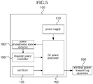
- FIG. 5 is a block diagram showing the power supply device 100 according to one embodiment.
- the power supply device 100 includes a power supply 110, an oscillator 130, an AC power generator 150, a power transmission state detector 180, and a transmit power controller 190.
- the power supply device 100 is connected with the wireless power transmitting apparatus 200.
- the power supply 110 generates DC power having DC voltage and outputs the DC power through an output terminal thereof.
- the oscillator 130 generates a lower-power sine wave signal.
- the power transmission state detector 180 detects a wireless power transmission state between the wireless power transmitting apparatus 200 and the wireless power transmitting apparatus 300.
- the transmit power controller 190 generates a control signal to control the AC power generator 150 based on the detected wireless power transmission state.
- the AC power generator 150 generates an AC power.
- the AC power can have various waveforms such as a rectangular-waveform, sinusoidal-waveform, or etc.
- the AC power generator 150 generates AC power having rectangular-waveform voltage by amplifying the lower-power sine wave signal of the oscillator 130 using DC power of the power supply 110 based on the control signal of the transmit power controller 190.
- the wireless power transmitting apparatus 200 transmits the output power of the AC power generator 150 to the wireless power receiving apparatus 300 by resonance.
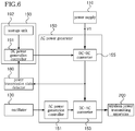
- FIG. 6 is a block diagram showing the AC power generator 150 and the transmit power controller 190 according to one embodiment.
- the AC power generator 150 includes AC power generation controller 151, a DC-AC converter 153, and a DC-DC converter 155, and the transmit power controller 190 includes a DC power generation controller 191 and a storage unit 192.
- the AC power generation controller 151 generates an AC power generation control signal based on the lower-power sine wave signal of the oscillator 130.
- the DC power generation controller 191 generates a DC power generation control signal based on the detected wireless power transmission state so that the DC-DC converter 155 may output power having output current in a target current range and target DC voltage.
- the storage unit 192 stores a look-up table.
- the DC-DC converter 155 converts the output power of the power supply 110 into DC power, which has output current in the target current range and the target DC voltage, based on the DC power generation control signal.
- the DC-AC converter 153 converts the output power of the DC-DC converter 155 into AC power having the rectangular-waveform AC voltage based on the AC power generation control signal, and outputs the power to the transmission induction coil unit 210.
- FIG. 7 is a circuit diagram showing the DC-DC converter 155 according to one embodiment.
- the DC-DC converter 155 includes an inductor L11, a power switch T11, a diode D11, and a capacitor C11.
- the power switch T11 may be realized by using a transistor.
- the power switch T11 may include an n-channel metal-oxide-semiconductor field-effect transistor (NMOSFET), but may be substituted with another device performing the same function.
- NMOSFET metal-oxide-semiconductor field-effect transistor
- One terminal of the inductor L11 is connected with an output terminal of the power supply 110, and an opposite terminal of the inductor L11 is connected with a drain electrode of the power switch T11.
- the gate electrode of the power switch T11 is connected with an output terminal of the DC power generation controller 191, and a source electrode of the power switch T11 is connected with the ground.
- An anode electrode of the diode D11 is connected with the drain electrode of the power switch T11.
- One terminal of the capacitor C11 is connected with the cathode electrode of the diode D11, and an opposite terminal of the capacitor C11 is connected with the ground.
- FIG. 8 is a circuit diagram showing the DC-AC converter 153 and the power transmission state detector 180 according to one embodiment.
- the DC-AC converter 153 includes a transistor circuit unit having a half-bridge structure.
- the half-bridge transistor circuit includes an upper transistor T21, a lower transistor T22, and a DC cut-off capacitor C21, and is connected to the AC power generation controller 151 and the transmission induction coil unit 210.
- the power transmission state detector 180 includes a resistor R1 and a voltage difference measuring unit 181, and is connected with the DC-DC converter 155, the DC-AC converter 153, and the DC power generation controller 191.
- the DC-AC converter 153 is connected with the DC-DC converter 155 through the resistor R1.
- the upper and lower transistors T21 and T22 may include n-channel metal-oxide-semiconductor field-effect transistor (NMOS), but may be substituted with another device performing the same function.
- NMOS metal-oxide-semiconductor field-effect transistor
- the AC power generation controller 151 has an output terminal for an upper transistor control signal and an output terminal for a lower transistor control signal, and outputs the AC power generation control signal based on the lower-power sine wave signal.
- the AC power generation controller 151 generates the upper transistor control signal as the AC power generation control signal based on the lower-power sine wave signal of the oscillator 130, and outputs the upper transistor control signal through the output terminal for the upper transistor control signal.
- the AC power generation controller 151 generates the lower transistor control signal as the AC power generation control signal based on the lower-power sine wave signal of the oscillator 130, and outputs the lower transistor control signal through the output terminal for the lower transistor control signal.
- a drain electrode of the upper transistor T21 is connected with one terminal of the resistor R1, and the gate electrode is connected with the output terminal for the upper transistor control signal of the AC power generation controller 151.
- a drain electrode of the lower transistor T22 is connected with a source electrode of the upper transistor T21, a gate electrode of the lower transistor T22 is connected with the output terminal for the lower transistor control signal of the AC power generation controller 151, and a source electrode of the lower transistor T22 is connected with the ground.
- One terminal of the DC cut-off capacitor C21 is connected with the source electrode of the upper transistor T21, and an opposite terminal of the DC cut-off capacitor C21 is connected with one terminal of the inductor L1. An opposite terminal of the inductor L1 is connected with the ground.
- the voltage difference measuring unit 181 measures the difference between voltages applied to both terminals of the resistor R1.
- FIG. 9 is a flowchart showing the wireless power transmitting method according to one embodiment
- FIG. 10 shows waveforms of voltage at each node in the power supply device 100 according to one embodiment.
- FIG. 9 shows the wireless power transmitting method to explain the embodiments of FIGS. 6 to 8 in detail.
- the power supply 110 generates DC power having DC voltage (step S101).
- the power supply 110 may convert AC power having AC voltage into the DC power having DC voltage.
- the oscillator 130 generates the lower-power sine wave signal (step S103).
- the power transmission state detector 180 detects the wireless power transmission state (step S105).
- the power transmission state detector 180 may detect the wireless power transmission state based on the level of the output current of the DC-DC converter 155. Since the voltages applied to the both terminal of the resistor R1 are proportional to the level of the output current of the DC-DC converter 155, the voltage difference measuring unit 181 of the power transmission state detector 180 may detect the wireless power transmission state based on the different between the voltages applied to both terminals of the resistor R1.
- the wireless power transmission state may be changed. In other words, as the distance between the distance between the wireless power transmitting apparatus 200 and the wireless power reception apparatus 300 is increased, the coupling coefficient is reduced, so that the wireless power transmission state may be degraded. As the wireless power transmission state becomes degraded, even if the wireless power transmitting apparatus 200 transmits power having the same intensity to the wireless power receiving apparatus 300, greater power is consumed due to the inferior transmission efficiency. Therefore, the power transmission state detector 180 may detect the wireless power transmission state based on the level of the output current of the DC-DC converter 155.
- the power transmission state detector 180 may measure the peak-to-peak value of the output current of the DC-DC converter 155.
- the DC power generation controller 191 generates a DC power generation control signal based on the detected wireless power transmission state so that the DC-DC converter 155 may output DC power having output current in a target current range and target DC voltage (step S107), and outputs the DC power generation control signal to the gate electrode of the transistor T11.
- the target current range may have a constant value regardless of the level of the target DC voltage, or may vary depending on the level of the target DC voltage.
- the target current range may be the range of the peak-to-peak value of the target current.
- the DC power generation control signal may be a pulse width modulation (PWM) signal continuously represented throughout the whole duration.
- PWM pulse width modulation
- the DC power generation controller 191 may determine a duty ratio of the PWM signal based on the detected wireless power transmission state.
- the voltage difference measuring unit 181 obtains a measurement output current value based on the difference between voltages applied to both terminals of the resistor R1. Thereafter, if the measurement output current value gets out of the reference range, the DC power generation controller 191 changes the duty rate, and outputs the DC power generation control signal serving as the PWM signal having the changed duty rate to the gate electrode of the transistor T11 so that the output current value of the DC-DC converter 155 becomes in the reference range.
- the DC power generation controller 191 reduces the duty rate and outputs the DC power generation control signal serving as the PWM signal having the reduced duty rate to the gate electrode of the transistor T11 so that the output current value of the DC-DC converter 155 becomes in the reference range. Further, if the measurement output current value is smaller than the lower limit of the reference range, the DC power generation controller 191 increases the duty rate and outputs the DC power generation control signal serving as the PWM signal having the increased duty rate to the gate electrode of the transistor T11 so that the output current value of the DC-DC converter 155 becomes in the reference range.
- the storage unit 192 may have a look-up table representing the relationship between a plurality of measurement output power values and a plurality of target output voltage values.
- Table 1 shows the look-up table representing the relationship between the measurement output power values and the target output voltage values according to one embodiment.
- Table 1 Measurement Output Power Target Output Voltage 10 W or less 12 V 10 ⁇ 12 W 14 V 12 ⁇ 14 W 16 V 14 ⁇ 16 W 18 V 16 ⁇ 18 W 20 V 18 ⁇ 20 W 22 V 20 W or more 24 V
- the voltage difference measuring unit 181 obtains a measurement output current value based on the difference between voltages applied to both terminals of the resistor R1. Thereafter, the DC power generation controller 191 obtains a measurement output power value of present output power of the DC-DC converter 155 based on the measurement output current value, and searches for a target output voltage value corresponding to the measurement output power value in the look-up table. Then, the duty rate of the PWM signal is determined using the voltage of the node B as feed-back information so that the output voltage of the DC-DC converter 155 may have the target output voltage value, and the DC power generation control signal may be generated based on the duty rate.
- the storage unit 192 may have a look-up table representing the relationship between a plurality of measurement output current values and a plurality of target output voltage values.
- the voltage difference measuring unit 181 obtains a measurement output current value based on the difference between voltages applied to both terminals of the resistor R1.
- the DC power generation controller 191 searches for a target output voltage value corresponding to the measurement output current value in the look-up table.
- the duty rate of the PWM signal is determined using the voltage of the node B as feed-back information so that the output voltage of the DC-DC converter 155 may have the target output voltage value, and the DC power generation control signal may be generated based on the duty rate.
- Table 2 shows a look-up table according to one embodiment.
- Table 2 Measurement output current at initial output voltage Coupling coefficient Target output voltage Desirable current range 100 mA or less 0.03 or less 30 V 801 ⁇ 851 mA 101 ⁇ 150 mA 0.05 28 V 751 ⁇ 800 mA 151 ⁇ 200 mA 0.08 26 V 701 ⁇ 751 mA 201 ⁇ 250 mA 0.11 24 V 651 ⁇ 700 mA 251 ⁇ 300 mA 0.14 22 V 601 ⁇ 650 mA 301 ⁇ 350 mA 0.17 20 V 551 ⁇ 600 mA 351 mA or more 0.20 or more 18 V 501 ⁇ 550 mA
- the storage unit 192 may have a look-up table corresponding to an output current value of the DC-DC converter 155, a coupling coefficient, an output voltage value of the DC-DC converter 155, and a desirable current range.
- the wireless power receiving apparatus 300 may be regarded as being detected.
- the initial output voltage may be 12V which is given for the illustrative purpose.
- the DC power generation controller 191 determines the wireless power receiving apparatus 300 as being apart from the wireless power transmitting apparatus 200 and controls the DC-DC converter 155 to have the output voltage of 28V.
- the DC power generation controller 191 determines if the level of the output current of the DC-DC converter 155 is in a desirable current range of 751 mA to 800 mA.
- the DC power generation controller 191 controls the DC-DC converter 155 so that the level of the output voltage of the DC-DC converter 155 is the level (12V) of the initial output voltage. If the level of the output current of the DC-DC converter 155 is 180 mA, the controller 270 determines the wireless power transmitting apparatus 200 as being closer to the wireless power receiving apparatus 300 when comparing with the case that the level of the output current of the DC-DC converter 155 is 120 mA. Accordingly, the controller 270 controls the DC-DC converter 155 such that the level of the output voltage of the DC-DC converter 155 is 26V.
- the distance between the wireless power transmitting apparatus 200 and the wireless power receiving apparatus 300 is related to the intensity of current
- various wireless power states such as a direction in which the wireless power transmitting apparatus 200 and the wireless power receiving apparatus 300 are placed may be considered.
- the wireless power transmitting apparatus 200 adjusts power transmitted to the wireless power receiving apparatus 300 based on the various wireless power transmission states such as the distance from the wireless power receiving apparatus 300 and the direction in which the wireless power receiving apparatus 300 is placed, thereby maximizing the power transmission efficiency, and presenting the power loss.
- the DC-DC converter 155 converts the output power of the power supply 110 into the DC power having the output current in the target current range and the target DC voltage based on the DC power generation control signal (step S109).
- the level of the output voltage of the DC-DC converter 155 may be equal to that of the output voltage of the power supply 110, or greater than or smaller than that of the output voltage of the power supply 110.
- the AC power generation controller 151 generates an AC power generation control signal based on the sin-wave lower power of the oscillator 130 (step S111).
- the AC power generation controller 151 may generate the upper transistor control signal serving as the AC power generation control signal based on the sin-wave lower power of the oscillator 130, and may output the upper transistor control signal through the output terminal for the upper transistor control signal.
- the AC power generation controller 151 may generate the lower transistor control signal serving as the AC power generation control signal based on the sin-wave lower power of the oscillator 130, and may output the lower transistor control signal through the output terminal for the lower transistor control signal.
- the upper and lower transistor control signals have the rectangular waveform.
- One period of the upper transistor control signal sequentially includes a turn-on time slot of the upper transistor T21 and a turn-off time slot of the upper transistor T21.
- the turn-on time slot of the upper transistor T21 may correspond to one half period of the lower-power sine wave signal of the oscillator 130, and the turn-off time slot of the upper transistor T21 may correspond to the other half period of the lower-power sine wave signal.
- One period of the lower transistor control signal sequentially includes a turn-on time slot of the lower transistor T22 and a turn-off time slot of the lower transistor T22.
- the turn-on time slot of the lower transistor T22 may correspond to one half period of the lower-power sine wave signal of the oscillator 130, and the turn-off time slot of the lower transistor T22 may correspond to the other half period of the lower-power sine wave signal.
- the upper transistor control signal has a level to turn on the upper transistor T21 during the turn-on time slot of the upper transistor T21.
- the level to turn on the upper transistor T21 may be a high level.
- the upper transistor control signal has a level to turn off the upper transistor T21.
- the level to turn off the upper transistor T21 may be a low level.
- the lower transistor control signal has a level to turn on the lower transistor T22.
- the level to turn on the lower transistor T22 may be a high level.
- the lower transistor control signal has a level to turn off the lower transistor T22.
- the level to turn off the lower transistor T22 may be a low level.
- the lower transistor control signal has the level to turn off the lower transistor T22 during the turn-off time slot of the lower transistor T22.
- the lower transistor control signal has the level to turn off the lower transistor T22 during the turn-off time slot of the upper transistor T21.
- the upper and lower transistor control signals may have a dead time slot.
- the turn-on time slot of the upper transistor T21 has a duration corresponding to (50-a)% of one period (T), and the dead time slot of the upper transistor T21 has the duration of a% of one period (T).
- the turn-off time slot of the upper transistor T21 may have a duration corresponding to 50% of one period (T)
- the turn-on time slot of the lower transistor T22 may have a duration corresponding to (50-a)% of one period (T)
- the dead time slot of the lower transistor T22 may have a duration corresponding to a% of one period (T)
- the turn-off time slot of the lower transistor T22 may have a duration corresponding to 50% of one period (T).
- "a" may be 1%.
- the DC-AC converter 153 converts the output power of the DC-DC converter 155 into AC power having rectangular-waveform AC voltage based on the AC power generation control signal (step S113) and outputs the AC power to the transmission induction coil unit 210.
- the upper and lower transistors T21 and T22 output rectangular-waveform power having rectangular-waveform voltage V3 shown in FIG. 10 according to the upper and lower transistor control signals having the dead time slot.
- the DC cut-off capacitor C21 cuts off DC voltage of the rectangular-waveform power and outputs the rectangular-waveform power having the rectangular-waveform AC voltage V4 to the transmission induction coil unit 210.
- the wireless power transmitting apparatus 200 transmits the rectangular-waveform AC power having the rectangular-waveform AC voltage to the wireless power receiving apparatus 300 by resonance (step S115).
- FIG. 11 is a block diagram showing the power supply device 100 according to another embodiment.
- the power supply device 100 includes the power supply 110, the oscillator 130, an AC power generator 160, the power transmission state detector 180, and the transmit power controller 190.
- the power supply device 100 is connected with the wireless power transmitting apparatus 200.
- the power supply 110 generates DC power having DC voltage and outputs the DC power through an output terminal thereof.
- the oscillator 130 generates a lower-power sine wave signal.
- the power transmission state detector 180 detects the wireless power transmission state.
- the transmit power controller 190 generates a control signal to control the AC power generator 160 based on the detected wireless power transmission state and the lower-power sine wave signal of the oscillator 130.
- the AC power generator 160 generates AC power having rectangular-waveform voltage by amplifying the lower-power sine wave signal of the oscillator 130 using DC power of the power supply 110 based on the control signal of the transmit power controller 190.
- the wireless power transmitting apparatus 200 transmits the output power of the AC power generator 160 to the wireless power receiving apparatus 300 by resonance.
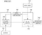
- FIG. 12 is a block diagram showing the AC power generator 160 and the transmit power controller 190 according to another embodiment.
- the AC power generator 160 includes a DC-AC converter 163, and the transmit power controller 190 includes an AC power generation controller 193.
- the AC power generation controller 193 generates an AC power generation control signal based on the lower-power sine wave signal of the oscillator 130. In addition, the AC power generation controller 193 may generate the AC power generation control signal, which allows the power supply 110 to output DC power having output current in a target current range, based on the detected wireless power transmission state.
- the target current range may be the range of the peak-to-peak value of the target current.
- the DC-AC converter 163 converts the output power of the power supply 110 into AC power having rectangular-waveform AC voltage based on the AC power generation control signal, and outputs the AC power to the transmission induction coil unit 210.
- FIG. 13 is a circuit diagram showing the DC-AC converter 163 and the power transmission state detector 180.
- the DC-AC converter 163 includes a full-bridge transistor circuit unit.
- the full-bridge transistor circuit unit includes two half-bridge transistor circuits.
- One of the two half-bridge transistor circuits includes upper and lower transistors T41 and T42, and the other includes upper and lower transistors T44 and T43.
- the upper transistors T41 and T44, and the lower transistors T42 and T43 may be n-channel metal-oxide-semiconductor field-effect transistors (NMOS-FETs), and may be substituted with different devices performing the same operation.
- NMOS-FETs n-channel metal-oxide-semiconductor field-effect transistors
- the power transmission state detector 180 includes a resistor R1 and the voltage difference measuring unit 181, and is connected to the power supply 110, the DC-AC converter 163, and the AC power generation controller 193.
- the DC-AC converter 163 is connected to the power supply 110 through the resistor R1.
- the AC power generation controller 193 has first and second upper transistor control signal output terminals and first and second lower transistor control signal output terminals, and generates an AC power generation control signal based on the lower-power sine wave signal of the oscillator 130 and a wireless power transmission state.
- a drain electrode of the upper transistor T41 is connected with one terminal of the resistor R1, a gate electrode of the upper transistor T41 is connected with the first upper transistor control signal output terminal of the AC power generation controller 193, and a source electrode of the upper transistor T41 is connected with one terminal of the inductor L1.
- a drain electrode of the lower transistor T42 is connected with the source electrode of the upper transistor T41, a gate electrode of the lower transistor T42 is connected to the first lower transistor control signal output terminal of the AC power generation controller 193, and a source electrode of the lower transistor T42 is connected with the ground.
- a drain electrode of the upper transistor T44 is connected with one terminal of the resistor R1, a gate electrode of the upper transistor T44 is connected with the second upper transistor control signal output terminal of the AC power generation controller 193, and a source electrode of the upper transistor T44 is connected with an opposite terminal of the inductor L1.
- a drain electrode of the lower transistor T43 is connected with the source electrode of the upper transistor T44, a gate electrode of the lower transistor T43 is connected to the second lower transistor control signal output terminal of the AC power generation controller 193, and a source electrode of the lower transistor T43 is connected with the ground.
- the voltage difference measuring unit 181 measures the difference between voltages applied to both terminals of the resistor R1.
- FIG. 14 is a flowchart showing the wireless power transmitting method according to another embodiment
- FIG. 15 shows waveforms of voltage at each node in the power supply device 100 according to another embodiment.
- FIG. 14 shows the wireless power transmitting method to explain the embodiments of FIGS. 11 to 13 in detail.
- the power supply 110 generates DC power having DC voltage (step S301).
- the power supply 110 may convert AC power having AC voltage into the DC power having DC voltage.
- the oscillator 130 generates a lower-power sine wave signal (step S303).
- the power transmission state detector 180 detects the wireless power transmission state (step S305).
- the power transmission state detector 180 may detect the wireless power transmission state based on the level of the output current of the power supply 110. Since the voltages applied to the both terminal of the resistor R1 are proportional to the level of the output current of the power supply 110, the voltage difference measuring unit 181 of the power transmission state detector 180 may detect the wireless power transmission state based on the different between the voltages applied to both terminals of the resistor R1. Since the output current of the power supply 110 may not be constantly maintained, the power transmission state detector 180 may measure the wireless power transmission state based on the peak-to-peak level of the output current of the power supply 110.
- the AC power generation controller 193 generates the AC power generation control signal allowing the power supply 110 to output DC power having the output current in the target current range, based on the detected wireless power transmission state (step S311), and outputs the generates the AC power generation control signal to the DC-AC converter 163. Since the output current of the power supply 110 may not be constantly maintained, the power transmission state detector 180 may measure the peak-to-peak level of the output current of the power supply 110.
- the AC power generation controller 193 may determine an operating mode of the DC-AC converter 163 based on the detected wireless power transmission state, and may output the AC power generation control signal for the operating mode to the DC-AC converter 163.
- the operating mode may be one of a full-bridge operating mode and a half-bridge operating mode.
- the voltage difference measuring unit 181 obtains a measurement output current value based on the difference between voltages applied to both terminals of the resistor R1.
- the DC power generation controller 191 may compare the measurement output current value with a reference value and determine the operating mode of the DC-AC converter 163 according to the comparison result.
- the reference value may be in the desirable current range of table 2 set according to the initial output voltage values.
- the DC power generation controller 191 may determine the operating mode of the DC-AC converter 163 as the full-bridge operating mode. If the measurement output current value is smaller than the reference value, the DC power generation controller 191 may determine the operating mode of the DC-AC converter 163 as the half-bridge operating mode.
- the AC power generation controller 193 operates one of two half-bridge transistor circuits, and stops the operation of the other.
- the AC power generation controller 193 turns off the upper transistor of the half-bridge transistor circuit, the operation of which is stopped, and turns on the lower transistor of the half-bridge transistor circuit.
- the AC power generation controller 193 applies a control signal to the half-bridge transistor circuit, the operation of which is allowed, as described with reference to FIG. 10 .
- the AC power generation controller 193 alternately applies a control signal for one half period and a control signal for the other half period to the DC-AC converter 163.
- the upper transistor T41 of one half-bridge transistor circuit is turned on, and the lower transistor T42 thereof is turned off.
- the upper transistor T44 of the other half-bridge transistor circuit is turned off, and the lower transistor T43 thereof is turned on.
- the upper transistor T41 of one half-bridge transistor circuit is turned off, and the lower transistor T42 thereof is turned on.
- the upper transistor T44 of the other half-bridge transistor circuit is turned on, and the lower transistor T43 thereof is turned off.
- Two transistor operating modes may be synchronized with a lower-power sine wave signal of the oscillator 130.
- the upper and lower transistor control signals may have a dead time slot.
- the voltage difference measuring unit 181 may obtain the measurement output current value based on the difference between voltages applied to both terminals of the resistor R1, the DC power generation controller 191 may obtain a measurement output power value, which is a present output power value of the power supply 110, based on the measurement output current value, and may determine the operating mode of the DC-AC converter 163 based on the measurement output power value.
- the operating mode may be one of the full-bridge operating mode and the half-bridge operating mode.
- the DC power generation controller 191 may compare the measurement output power value with the reference value and determine the operating mode of the DC-AC converter 163 according to the comparison result.
- the reference value may be in the desirable current range of table 2 set according to the initial output voltage value.
- the DC power generation controller 191 may determine the operating mode of the DC-AC converter 163 as a full-bridge operating mode. If the measurement output power value is smaller than the reference value, the DC power generation controller 191 may determine the operating mode of the DC-AC converter 163 as the half-bridge operating mode.
- the DC-AC converter 163 converts the output power of the power supply 110 into the AC power having the rectangular-waveform AC voltage V3 based on the AC power generation control signal (step S313), and outputs the output power to the transmission induction coil unit 210.
- the wireless power transmitting apparatus 200 transmits the rectangular-waveform AC power having the rectangular-waveform AC voltage V3 to the wireless power receiving apparatus 300 by resonance (step S315).
- FIG. 16 is a block diagram showing the power supply device 100 according to still another embodiment.
- the power supply device 100 includes a power supply 110, an oscillator 130, an AC power generator 170, a power transmission state detector 180, and a transmit power controller 190.
- the power supply device 100 is connected with the wireless power transmitting apparatus 200.
- the power supply 110 generates DC power having DC voltage and outputs the DC power through an output terminal thereof.
- the oscillator 130 generates a lower-power sine wave signal.
- the power transmission state detector 180 detects the wireless power transmission state.
- the transmit power controller 190 generates a control signal to control the AC power generator 170 based on the detected wireless power transmission state and the lower-power sine wave signal of the oscillator 130.
- the AC power generator 170 generates AC power having rectangular-waveform voltage by amplifying the lower-power sine wave signal of the oscillator 130 using DC power of the power supply 110 according to the control signal of the transmit power controller 190.
- the wireless power transmitting apparatus 200 transmits the output power of the AC power generator 170 to the wireless power receiving apparatus 300 by resonance.
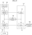
- FIG. 17 is a block diagram showing the AC power generator 170 and the transmit power controller 190 according to still another embodiment.
- the AC power generator 170 includes a DC-DC converter 175 and a DC-AC converter 173, and the transmit power controller 190 includes an DC power generation controller 191, a storage unit 192, and an AC power generation controller 193.
- the DC power generation controller 191 generates a DC power generation control signal based on the detected wireless power transmission state so that the DC-DC converter 175 may output DC power having output current in a target current range and target DC voltage.
- the storage unit 192 stores a look-up table.
- the DC-DC converter 175 converts the output power of the power supply 110 into the DC power, which has output current in the target current range and the target DC voltage, based on the DC power generation control signal.
- the AC power generation controller 193 generates an AC power generation control signal based on the lower-power sine wave signal of the oscillator 130. In addition, the AC power generation controller 193 may generate the AC power generation control signal, which allows the DC-DC converter 175 to output DC power having the output current in the target current range, based on the detected wireless power transmission state.
- the target current range may be the range of the peak-to-peak value of the target current.
- the DC-AC converter 173 converts the output power of the DC-DC converter 155 into the rectangular-waveform power based on the AC power generation control signal, and outputs the power to the transmission induction coil unit 210.
- FIG. 18 is a circuit diagram showing the DC-AC converter 173 and the power transmission state detector 180 according to still another embodiment.
- the DC-AC converter 173 includes a full-bridge transistor circuit unit.
- the full-bridge transistor circuit unit includes two half-bridge transistor circuits.
- One of the two half-bridge transistor circuits includes upper and lower transistors T61 and T62, and the other includes upper and lower transistors T64 and T63.
- the upper transistors T61 and T64, and the lower transistors T62 and T63 may be n-channel metal-oxide-semiconductor field-effect transistors (NMOS-FETs), and may be substituted with different devices performing the same operation.
- NMOS-FETs n-channel metal-oxide-semiconductor field-effect transistors
- the power transmission state detector 180 includes a resistor R1 and the voltage difference measuring unit 181, and is connected to the DC-DC converter 175, the DC-AC converter 173, and the AC power generation controller 193.
- the DC-AC converter 173 is connected to the DC-DC converter 175 through the resistor R1.
- the AC power generation controller 193 has first and second upper transistor control signal output terminals and first and second lower transistor control signal output terminals, and generates an AC power generation control signal based on the lower-power sine wave signal of the oscillator 130 and a wireless power transmission state.
- a drain electrode of the upper transistor T61 is connected with one terminal of the resistor R1, a gate electrode of the upper transistor T61 is connected with the first upper transistor control signal output terminal of the AC power generation controller 193, and a source electrode of the upper transistor T61 is connected with one terminal of the inductor L1.
- a drain electrode of the lower transistor T62 is connected with the source electrode of the upper transistor T61, a gate electrode of the lower transistor T62 is connected to the first lower transistor control signal output terminal of the AC power generation controller 193, and a source electrode of the lower transistor T62 is connected with the ground.
- a drain electrode of the upper transistor T64 is connected with one terminal of the resistor R1, a gate electrode of the upper transistor T64 is connected with the second upper transistor control signal output terminal of the AC power generation controller 193, and a source electrode of the upper transistor T64 is connected with an opposite terminal of the inductor L1.
- a drain electrode of the lower transistor T63 is connected with the source electrode of the upper transistor T64, a gate electrode of the lower transistor T63 is connected to the second lower transistor control signal output terminal of the AC power generation controller 193, and a source electrode of the lower transistor T63 is connected with the ground.
- the voltage difference measuring unit 181 measures the difference between voltages applied to both terminals of the resistor R1.
- FIG. 19 is a flowchart showing the wireless power transmitting method according to still another embodiment.
- FIG. 19 shows the wireless power transmitting method to explain the embodiments of FIGS. 16 to 18 in detail.
- the power supply 110 generates DC power having DC voltage (step S501).
- the power supply 110 may convert AC power having AC voltage into the DC power having DC voltage.
- the oscillator 130 generates the lower-power sine wave signal (step S503).
- the power transmission state detector 180 detects the wireless power transmission state (step S505).
- the power transmission state detector 180 may detect the wireless power transmission state based on the level of the output current of the DC-DC converter 175. Since the voltages applied to the both terminal of the resistor R1 are proportional to the level of the output current of the power supply 110, the voltage difference measuring unit 181 of the power transmission state detector 180 may detect the wireless power transmission state based on the different between the voltages applied to both terminals of the resistor R1. Since the output current of the DC-DC converter 175 may not be constantly maintained, the power transmission state detector 180 may measure the peak-to-peak value of the output current of the DC-DC converter 175.
- the DC power generation controller 191 generates a DC power generation control signal based on the detected wireless power transmission state so that the DC-DC converter 175 may output DC power having current in the target current range and target DC voltage (step S507), and outputs the DC power generation control signal to the gate electrode of the transistor T11. Details of step S507 have already been described in step S107.
- the DC-DC converter 175 converts the output power of the power supply 110 into DC power having the output current in the target current range and the target DC voltage based on the DC power generation control signal (step S509).
- the AC power generation controller 193 generates the AC power generation control signal allowing the DC-DC converter 175 to output DC power having the output current in the target current range, based on the detected wireless power transmission state (step S511), and outputs the AC power generation control signal to the DC-AC converter 173. Details of step S511 have already been described in step S311.
- the DC-AC converter 173 converts the output power of the power supply 110 into the AC power having the rectangular-waveform AC voltage V3 based on the AC power generation control signal (step S513), and outputs the output power to the transmission induction coil unit 210.
- the wireless power transmitting apparatus 200 transmits the rectangular-waveform AC power having the rectangular-waveform AC voltage V3 to the wireless power receiving apparatus 300 by resonance (step S515).
- any reference in this specification to "one embodiment,” “an embodiment,” “example embodiment,” etc. means that a particular feature, structure, or characteristic described in connection with the embodiment is included in at least one embodiment of the invention.
- the appearances of such phrases in various places in the specification are not necessarily all referring to the same embodiment.
Landscapes
- Engineering & Computer Science (AREA)
- Computer Networks & Wireless Communication (AREA)
- Power Engineering (AREA)
- Signal Processing (AREA)
- Charge And Discharge Circuits For Batteries Or The Like (AREA)
- Inverter Devices (AREA)
Claims (9)
- Drahtlos-Stromübertragungsvorrichtung (200) zur drahtlosen Übertragung von Strom an eine Drahtlos-Stromempfangsvorrichtung (300), wobei die Drahtlos-Stromübertragungsvorrichtung (200) folgendes umfasst:- einen Detektor (180) zur Detektion eines Drahtlos-Stromübertragungszustandes zwischen der Drahtlos-Stromübertragungsvorrichtung (200) und der Drahtlos-Stromempfangsvorrichtung (300);- einen Sendeleistungsregler (190) zur Erzeugung eines Steuersignals zur Steuerung der Sendeleistung entsprechend dem detektierten Drahtlos-Stromübertragungszustand;- einen Wechselstromgenerator (150) zur Erzeugung eines Wechselstroms mittels eines ersten Gleichstroms entsprechend dem Steuersignal; und- eine Übertragungs-Induktionsspuleneinheit zur Übertragung des Wechselstroms an eine Übertragungsresonanzspule über ein elektromagnetisches Induktionssystem,wobei der Wechselstromgenerator (150) folgendes umfasst:- einen DC/DC-Wandler (155) zur Umwandlung des ersten Gleichstroms in einen zweiten Gleichstrom entsprechend dem Steuersignal; und- einen DC/AC-Wandler (153) zur Umwandlung des zweiten Gleichstroms in Wechselstrom, wobei der Detektor (180) dazu dient, den Drahtlos-Stromübertragungszustand anhand eines Pegels des Ausgangsstroms des DC/DC-Wandlers (155) zu detektieren,dadurch gekennzeichnet, dass der Sendeleistungsregler (190) folgendes umfasst:- eine Speichereinheit (192) zur Speicherung einer Wertetabelle, wobei die Wertetabelle einen Zielwert der Ausgangsspannung enthält, der dem Pegel des Ausgangsstroms des DC/DC-Wandlers (155) entspricht; und- einen Gleichstromerzeugungsregler (191) zur Erzeugung des Steuersignals anhand des Zielwertes der Ausgangsspannung.
- Drahtlos-Stromübertragungsvorrichtung (200) nach Anspruch 1, wobei der Gleichstromerzeugungsregler (191) dazu dient, anhand des detektierten Drahtlos-Stromübertragungszustands ein DC-Stromerzeugungssteuersignal zu erzeugen, und der DC/DC-Wandler (155) dazu dient, den ersten Gleichstrom entsprechend dem DC-Stromerzeugungssteuersignal in den zweiten Gleichstrom umzuwandeln.
- Drahtlos-Stromübertragungsvorrichtung (200) nach Anspruch 2, wobei der Gleichstromerzeugungsregler (191) dazu dient, ein Tastverhältnis des DC-Stromerzeugungssteuersignals entsprechend dem detektierten Drahtlos-Stromübertragungszustands zu ändern.
- Drahtlos-Stromübertragungsvorrichtung (200) nach einem der Ansprüche 1 bis 3, wobei der DC/AC-Wandler (153) eine Transistorschaltungseinheit umfasst, die eine Halbbrückenstruktur aufweist.
- Drahtlos-Stromübertragungsvorrichtung (200) nach Anspruch 1, wobei der Wechselstromgenerator (150) eine Vollbrücken-Transistorschaltungseinheit umfasst, die in einem Halbbrücken-Betriebsmodus und einem Vollbrücken-Betriebsmodus betrieben werden kann.
- Drahtlos-Stromübertragungsvorrichtung (200) nach Anspruch 5, wobei der Sendeleistungsregler (190) einen Wechselstromerzeugungsregler (193) umfasst, der dazu dient, anhand des detektierten Drahtlos-Stromübertragungszustands ein AC-Stromerzeugungssteuersignal zu erzeugen, und die Vollbrücken-Transistorschaltungseinheit dazu dient, den zweiten Gleichstrom entsprechend dem AC-Stromerzeugungssteuersignal in Wechselstrom umzuwandeln.
- Drahtlos-Stromübertragungsvorrichtung (200) nach Anspruch 6, wobei der Wechselstromerzeugungsregler (193) dazu dient, entsprechend dem festgestellten Betriebsmodus ein AC-Stromerzeugungssteuersignal zu erzeugen.
- Drahtlos-Stromübertragungsvorrichtung (200) nach den Ansprüchen 1 bis 7, wobei der Detektor (180) dazu dient, den Drahtlos-Stromübertragungszustand anhand eines Spitze-Spitze-Pegels des Stroms der Sendeleistung zu detektieren.
- Drahtlos-Stromübertragungsvorrichtung (200) nach einem der Ansprüche 1 bis 8, wobei der Wechselstrom ein Rechteckwellenstrom ist.
Priority Applications (1)
| Application Number | Priority Date | Filing Date | Title |
|---|---|---|---|
| EP18155272.0A EP3340419B1 (de) | 2012-03-19 | 2013-03-15 | Vorrichtung zur drahtlosen stromübertragung und verfahren dafür |
Applications Claiming Priority (2)
| Application Number | Priority Date | Filing Date | Title |
|---|---|---|---|
| KR1020120027977A KR101438880B1 (ko) | 2012-03-19 | 2012-03-19 | 무선전력 송신장치 및 무선전력 전송 방법 |
| KR1020120146956A KR102019079B1 (ko) | 2012-12-14 | 2012-12-14 | 무선 전력 송신 장치 및 방법 |
Related Child Applications (2)
| Application Number | Title | Priority Date | Filing Date |
|---|---|---|---|
| EP18155272.0A Division EP3340419B1 (de) | 2012-03-19 | 2013-03-15 | Vorrichtung zur drahtlosen stromübertragung und verfahren dafür |
| EP18155272.0A Division-Into EP3340419B1 (de) | 2012-03-19 | 2013-03-15 | Vorrichtung zur drahtlosen stromübertragung und verfahren dafür |
Publications (2)
| Publication Number | Publication Date |
|---|---|
| EP2642628A1 EP2642628A1 (de) | 2013-09-25 |
| EP2642628B1 true EP2642628B1 (de) | 2018-05-02 |
Family
ID=47997024
Family Applications (2)
| Application Number | Title | Priority Date | Filing Date |
|---|---|---|---|
| EP13159585.2A Active EP2642628B1 (de) | 2012-03-19 | 2013-03-15 | Drahtlose Leistungsübertragungsvorrichtung und Verfahren davon |
| EP18155272.0A Active EP3340419B1 (de) | 2012-03-19 | 2013-03-15 | Vorrichtung zur drahtlosen stromübertragung und verfahren dafür |
Family Applications After (1)
| Application Number | Title | Priority Date | Filing Date |
|---|---|---|---|
| EP18155272.0A Active EP3340419B1 (de) | 2012-03-19 | 2013-03-15 | Vorrichtung zur drahtlosen stromübertragung und verfahren dafür |
Country Status (4)
| Country | Link |
|---|---|
| US (4) | US9225391B2 (de) |
| EP (2) | EP2642628B1 (de) |
| JP (2) | JP5643362B2 (de) |
| CN (1) | CN103326475B (de) |
Families Citing this family (49)
| Publication number | Priority date | Publication date | Assignee | Title |
|---|---|---|---|---|
| US9225391B2 (en) | 2012-03-19 | 2015-12-29 | Lg Innotek Co., Ltd. | Wireless power transmitting apparatus and method thereof |
| EP2709285A1 (de) * | 2012-09-17 | 2014-03-19 | ST-Ericsson SA | Verfahren und Empfänger für die Kommunikation während einer drahtlosen Leistungsübertragung |
| JP6067308B2 (ja) * | 2012-10-01 | 2017-01-25 | ローム株式会社 | ワイヤレス受電回路およびそれを用いた電子機器 |
| KR102008810B1 (ko) * | 2012-11-12 | 2019-08-08 | 엘지이노텍 주식회사 | 무선 전력 송신 장치 및 방법 |
| WO2015004806A1 (ja) * | 2013-07-12 | 2015-01-15 | 株式会社Ihi | 電力伝送システム |
| JP6503351B2 (ja) | 2013-07-29 | 2019-04-17 | アルフレッド イー. マン ファウンデーション フォー サイエンティフィック リサーチ | 埋め込み可能なデバイス用の高効率磁気リンク |
| WO2015017475A2 (en) | 2013-07-29 | 2015-02-05 | Alfred E. Mann Foundation For Scientific Research | Microprocessor controlled class e driver |
| EP2868516A1 (de) * | 2013-10-31 | 2015-05-06 | Brusa Elektronik AG | Verfahren zur Regelung der zwischen zwei Resonatoren eines Systems zur kontaktlosen Energieübertragung übertragenen Energie, sowie Resonatoranordnung |
| KR102146484B1 (ko) * | 2014-01-08 | 2020-08-21 | 엘지이노텍 주식회사 | 전력 생성 장치, 무선 전력 송신 장치 및 무선 전력 전송 시스템 |
| WO2015105334A1 (ko) * | 2014-01-08 | 2015-07-16 | 엘지이노텍 주식회사 | 무선 전력 송신 장치 및 무선 전력 전송 시스템 |
| KR102175599B1 (ko) * | 2014-01-24 | 2020-11-06 | 엘지이노텍 주식회사 | 무선전력전송 시스템 |
| KR20150089754A (ko) * | 2014-01-28 | 2015-08-05 | 엘지이노텍 주식회사 | 무선 전력 수신 장치 및 단말기 |
| JP6146333B2 (ja) * | 2014-02-13 | 2017-06-14 | 株式会社豊田自動織機 | 送電機器及び非接触電力伝送装置 |
| US9995777B2 (en) * | 2014-02-14 | 2018-06-12 | Qualcomm Incorporated | Device detection through dynamic impedance change measurement |
| WO2015127303A1 (en) | 2014-02-23 | 2015-08-27 | Apple Inc. | Impedance matching for inductive power transfer systems |
| AU2015218896B2 (en) | 2014-02-23 | 2018-03-29 | Apple Inc. | Adjusting filter in a coupled coil system |
| US9385537B2 (en) * | 2014-03-03 | 2016-07-05 | Divergent, Inc. | Using skin effect to produce a magnetic vector potential for inducing a voltage |
| US9373966B2 (en) | 2014-03-03 | 2016-06-21 | Divergent, Inc. | Wireless power and communication systems using magnetic vector potential |
| US9472366B2 (en) | 2014-03-03 | 2016-10-18 | Divergent, Inc. | Generation and use of electric fields from capacitive effects of a solenoid |
| KR102187437B1 (ko) | 2014-03-11 | 2020-12-08 | 엘지이노텍 주식회사 | 무선전력 전송 장치를 구비한 무선전력전송 시스템 |
| US10032557B1 (en) | 2014-05-29 | 2018-07-24 | Apple Inc. | Tuning of primary and secondary resonant frequency for improved efficiency of inductive power transfer |
| US9537353B1 (en) | 2014-06-03 | 2017-01-03 | Apple Inc. | Methods for detecting mated coils |
| US9369203B1 (en) | 2014-06-11 | 2016-06-14 | Google Inc. | Wirelessly powered passive optical power meter |
| US9685814B1 (en) | 2014-06-13 | 2017-06-20 | Apple Inc. | Detection of coil coupling in an inductive charging system |
| US9813041B1 (en) | 2014-07-31 | 2017-11-07 | Apple Inc. | Automatic boost control for resonant coupled coils |
| US10014733B2 (en) | 2014-08-28 | 2018-07-03 | Apple Inc. | Temperature management in a wireless energy transfer system |
| US10193372B2 (en) * | 2014-09-02 | 2019-01-29 | Apple Inc. | Operating an inductive energy transfer system |
| WO2016090530A1 (zh) * | 2014-12-08 | 2016-06-16 | 胡沥 | 无线充电装置及系统 |
| EP3235106A4 (de) * | 2014-12-18 | 2018-01-10 | PowerbyProxi Limited | Induktiver leistungssender und verfahren zur leistungsflusssteuerung |
| KR101663191B1 (ko) * | 2015-01-30 | 2016-10-07 | 한솔테크닉스(주) | 무선 전력 전송 기반의 가습장치 |
| JP6554317B2 (ja) * | 2015-05-18 | 2019-07-31 | ローム株式会社 | 同期整流回路、その制御回路、ワイヤレス受電装置および電子機器 |
| US10666084B2 (en) | 2015-07-10 | 2020-05-26 | Apple Inc. | Detection and notification of an unpowered releasable charging device |
| JP6569861B2 (ja) * | 2015-10-02 | 2019-09-04 | パナソニックIpマネジメント株式会社 | 無線電力伝送システム |
| US10164600B2 (en) * | 2015-10-12 | 2018-12-25 | Nxp B.V. | NFC or RFID device RF detuning detection and driver output power regulation |
| US9788282B2 (en) | 2015-11-30 | 2017-10-10 | Veniam, Inc. | Systems and methods for improving fixed access point coverage in a network of moving things |
| US9948512B2 (en) | 2016-01-14 | 2018-04-17 | Veniam, Inc. | Systems and methods for remote configuration update and distribution in a network of moving things |
| TWI605664B (zh) * | 2016-06-29 | 2017-11-11 | 立錡科技股份有限公司 | 諧振式無線電源發送電路及其控制方法 |
| WO2018048312A1 (en) * | 2016-09-06 | 2018-03-15 | Powerbyproxi Limited | An inductive power transmitter |
| US10644531B1 (en) | 2016-09-22 | 2020-05-05 | Apple Inc. | Adaptable power rectifier for wireless charger system |
| DE102016123268B3 (de) * | 2016-12-01 | 2018-03-01 | Lisa Dräxlmaier GmbH | Ladegerät und verfahren zum induktiven laden eines mobilen gerätes innerhalb eines kraftfahrzeuges |
| CN108242826A (zh) * | 2016-12-27 | 2018-07-03 | 全亿大科技(佛山)有限公司 | 无线充电发射器和无线充电方法 |
| US10389274B2 (en) | 2017-04-07 | 2019-08-20 | Apple Inc. | Boosted output inverter for electronic devices |
| US10523063B2 (en) | 2017-04-07 | 2019-12-31 | Apple Inc. | Common mode noise compensation in wireless power systems |
| US11038374B2 (en) * | 2017-04-18 | 2021-06-15 | Infineon Technologies Austria Ag | Flexible bridge amplifier for wireless power |
| CN109120075B (zh) * | 2017-06-22 | 2023-11-28 | 恩智浦美国有限公司 | 检测无线充电发送器的充电区域内物体的方法与装置 |
| JP2020065388A (ja) * | 2018-10-18 | 2020-04-23 | セイコーエプソン株式会社 | 制御装置、送電装置、無接点電力伝送システム、受電装置及び電子機器 |
| WO2020185902A1 (en) | 2019-03-11 | 2020-09-17 | Axonics Modulation Technologies, Inc. | Charging device with off-center coil |
| US11476898B2 (en) | 2021-01-28 | 2022-10-18 | Nucurrent, Inc. | Wireless power transfer system with mode switching using selective quality factor alteration |
| US11271611B1 (en) | 2021-01-28 | 2022-03-08 | Nucurrent, Inc. | Wireless power transfer with in-band virtualized wired communications |
Citations (1)
| Publication number | Priority date | Publication date | Assignee | Title |
|---|---|---|---|---|
| EP2286727A1 (de) * | 2009-08-17 | 2011-02-23 | Schleifring und Apparatebau GmbH | Gesteuerte kontaktfreie Leistungsübertragung |
Family Cites Families (30)
| Publication number | Priority date | Publication date | Assignee | Title |
|---|---|---|---|---|
| JP2803943B2 (ja) * | 1992-10-21 | 1998-09-24 | アルプス電気株式会社 | 非接触電力供給装置 |
| US5373432A (en) * | 1992-12-10 | 1994-12-13 | Hughes Aircraft Company | Fixed frequency DC to DC converter with a variable inductance controller |
| US5546295A (en) * | 1994-02-24 | 1996-08-13 | Rotron Incorporated | Electrical power converter, power supply, and inverter with series-connected switching circuits |
| JPH09182304A (ja) | 1995-12-26 | 1997-07-11 | Tdk Corp | 非接触型充電器 |
| JP3531385B2 (ja) | 1996-10-28 | 2004-05-31 | ソニー株式会社 | 電源装置 |
| CN2660781Y (zh) | 2003-09-22 | 2004-12-01 | 陈仁富 | 移相谐振软开关逆变器用控制驱动器 |
| US7443113B2 (en) * | 2003-12-02 | 2008-10-28 | Universal Lighting Technologies, Inc. | Software controlled electronic dimming ballast |
| JP4706036B2 (ja) | 2005-02-03 | 2011-06-22 | 学校法人東京理科大学 | 非接触電力供給システム及びそれを用いた医療システム |
| JP5062658B2 (ja) * | 2006-07-28 | 2012-10-31 | 東京エレクトロン株式会社 | 導波管内の定在波測定部および定在波測定方法、電磁波利用装置、プラズマ処理装置およびプラズマ処理方法 |
| US8729734B2 (en) | 2007-11-16 | 2014-05-20 | Qualcomm Incorporated | Wireless power bridge |
| KR101079822B1 (ko) | 2008-07-16 | 2011-11-04 | (주) 단 더휴네코리아 | 건축물용 조립식 바닥재 |
| US8278784B2 (en) | 2008-07-28 | 2012-10-02 | Qualcomm Incorporated | Wireless power transmission for electronic devices |
| DE112009001614T5 (de) * | 2008-08-26 | 2011-04-21 | Mitsubishi Electric Corporation | Entladungslampen-Vorschaltgerät-Apparat |
| US8446046B2 (en) | 2008-10-03 | 2013-05-21 | Access Business Group International Llc | Power system |
| TWI356566B (en) * | 2008-10-03 | 2012-01-11 | Ablerex Electronics Co Ltd | Ripple voltage suppression method for dc/dc conver |
| US8497658B2 (en) | 2009-01-22 | 2013-07-30 | Qualcomm Incorporated | Adaptive power control for wireless charging of devices |
| KR101041150B1 (ko) | 2009-01-30 | 2011-06-13 | 황인태 | 휴대폰 무접점 충전장치 |
| JP4865001B2 (ja) | 2009-04-13 | 2012-02-01 | 株式会社日本自動車部品総合研究所 | 非接触給電設備、非接触受電装置および非接触給電システム |
| US8374545B2 (en) | 2009-09-02 | 2013-02-12 | Qualcomm Incorporated | De-tuning in wireless power reception |
| US8928284B2 (en) | 2009-09-10 | 2015-01-06 | Qualcomm Incorporated | Variable wireless power transmission |
| US8729735B2 (en) | 2009-11-30 | 2014-05-20 | Tdk Corporation | Wireless power feeder, wireless power receiver, and wireless power transmission system |
| JP5672843B2 (ja) | 2009-11-30 | 2015-02-18 | Tdk株式会社 | ワイヤレス給電装置、ワイヤレス受電装置およびワイヤレス電力伝送システム |
| TWM385858U (en) | 2010-02-12 | 2010-08-01 | Fu Da Tong Technology Co Ltd | Frequency conversion type wireless power supply and charging device |
| US9561730B2 (en) * | 2010-04-08 | 2017-02-07 | Qualcomm Incorporated | Wireless power transmission in electric vehicles |
| KR101744162B1 (ko) | 2010-05-03 | 2017-06-07 | 삼성전자주식회사 | 소스-타겟 구조의 매칭을 제어하는 장치 및 방법 |
| US8829729B2 (en) * | 2010-08-18 | 2014-09-09 | Tdk Corporation | Wireless power feeder, wireless power receiver, and wireless power transmission system |
| KR101243587B1 (ko) * | 2011-02-17 | 2013-03-20 | 주식회사 팬택 | 무접점 충전 장치, 무접점 충전 시스템 및 무접점 충전 방법 |
| US20130026981A1 (en) * | 2011-07-28 | 2013-01-31 | Broadcom Corporation | Dual mode wireless power |
| US9041254B2 (en) * | 2011-12-14 | 2015-05-26 | Linear Technology Corporation | Primary unit control of resonant inductive power transfer system for optimum efficiency |
| US9225391B2 (en) | 2012-03-19 | 2015-12-29 | Lg Innotek Co., Ltd. | Wireless power transmitting apparatus and method thereof |
-
2013
- 2013-03-14 US US13/826,526 patent/US9225391B2/en active Active
- 2013-03-15 EP EP13159585.2A patent/EP2642628B1/de active Active
- 2013-03-15 EP EP18155272.0A patent/EP3340419B1/de active Active
- 2013-03-15 JP JP2013053241A patent/JP5643362B2/ja active Active
- 2013-03-19 CN CN201310088465.2A patent/CN103326475B/zh active Active
-
2014
- 2014-10-30 JP JP2014221116A patent/JP6153506B2/ja active Active
-
2015
- 2015-12-28 US US14/980,904 patent/US9711974B2/en not_active Ceased
-
2019
- 2019-07-12 US US16/510,270 patent/USRE49017E1/en active Active
-
2022
- 2022-02-18 US US17/675,619 patent/USRE49955E1/en active Active
Patent Citations (1)
| Publication number | Priority date | Publication date | Assignee | Title |
|---|---|---|---|---|
| EP2286727A1 (de) * | 2009-08-17 | 2011-02-23 | Schleifring und Apparatebau GmbH | Gesteuerte kontaktfreie Leistungsübertragung |
Also Published As
| Publication number | Publication date |
|---|---|
| US9225391B2 (en) | 2015-12-29 |
| EP3340419B1 (de) | 2020-08-19 |
| US20160111895A1 (en) | 2016-04-21 |
| USRE49955E1 (en) | 2024-04-30 |
| US9711974B2 (en) | 2017-07-18 |
| US20130241304A1 (en) | 2013-09-19 |
| JP5643362B2 (ja) | 2014-12-17 |
| EP2642628A1 (de) | 2013-09-25 |
| JP2015073432A (ja) | 2015-04-16 |
| EP3340419A1 (de) | 2018-06-27 |
| JP6153506B2 (ja) | 2017-06-28 |
| CN103326475B (zh) | 2015-08-26 |
| USRE49017E1 (en) | 2022-04-05 |
| JP2013198402A (ja) | 2013-09-30 |
| CN103326475A (zh) | 2013-09-25 |
Similar Documents
| Publication | Publication Date | Title |
|---|---|---|
| USRE49955E1 (en) | Wireless power transmitting apparatus and method thereof | |
| US10181756B2 (en) | Wireless power transmitter and power transmission method thereof | |
| US10063099B2 (en) | Wireless power receiver for controlling wireless power by using switch | |
| CN103259340B (zh) | 无线电力传送器、无线电力接收器、及电力传输方法 | |
| KR101428161B1 (ko) | 무선전력 수신장치 및 그의 전력 제어 방법 | |
| US10284018B2 (en) | System, apparatus and method for adaptive tuning for wireless power transfer | |
| US9680336B2 (en) | Wireless power repeater and method thereof | |
| US10148127B2 (en) | Wireless power transmitting apparatus and method thereof | |
| US10063085B2 (en) | Power supplying apparatus and wireless power transmitter | |
| US10411517B2 (en) | Wireless power transfer method, apparatus and system for low and medium power | |
| US9912194B2 (en) | Wireless power apparatus and operation method thereof | |
| US20190341797A1 (en) | Inductive Power Transfer System | |
| KR101835125B1 (ko) | 무선전력 수신장치 및 그의 전력 제어 방법 | |
| KR102019079B1 (ko) | 무선 전력 송신 장치 및 방법 | |
| KR20190096888A (ko) | 무선 전력 송신 장치 및 방법 |
Legal Events
| Date | Code | Title | Description |
|---|---|---|---|
| PUAI | Public reference made under article 153(3) epc to a published international application that has entered the european phase |
Free format text: ORIGINAL CODE: 0009012 |
|
| AK | Designated contracting states |
Kind code of ref document: A1 Designated state(s): AL AT BE BG CH CY CZ DE DK EE ES FI FR GB GR HR HU IE IS IT LI LT LU LV MC MK MT NL NO PL PT RO RS SE SI SK SM TR |
|
| AX | Request for extension of the european patent |
Extension state: BA ME |
|
| 17P | Request for examination filed |
Effective date: 20140313 |
|
| RBV | Designated contracting states (corrected) |
Designated state(s): AL AT BE BG CH CY CZ DE DK EE ES FI FR GB GR HR HU IE IS IT LI LT LU LV MC MK MT NL NO PL PT RO RS SE SI SK SM TR |
|
| 17Q | First examination report despatched |
Effective date: 20160704 |
|
| STAA | Information on the status of an ep patent application or granted ep patent |
Free format text: STATUS: EXAMINATION IS IN PROGRESS |
|
| RAP1 | Party data changed (applicant data changed or rights of an application transferred) |
Owner name: LG INNOTEK CO., LTD. |
|
| REG | Reference to a national code |
Ref country code: DE Ref legal event code: R079 Ref document number: 602013036773 Country of ref document: DE Free format text: PREVIOUS MAIN CLASS: H02J0005000000 Ipc: H02J0050100000 |
|
| GRAP | Despatch of communication of intention to grant a patent |
Free format text: ORIGINAL CODE: EPIDOSNIGR1 |
|
| STAA | Information on the status of an ep patent application or granted ep patent |
Free format text: STATUS: GRANT OF PATENT IS INTENDED |
|
| RIC1 | Information provided on ipc code assigned before grant |
Ipc: H02J 7/02 20160101ALI20170904BHEP Ipc: H02J 50/10 20160101AFI20170904BHEP |
|
| INTG | Intention to grant announced |
Effective date: 20171006 |
|
| GRAS | Grant fee paid |
Free format text: ORIGINAL CODE: EPIDOSNIGR3 |
|
| GRAA | (expected) grant |
Free format text: ORIGINAL CODE: 0009210 |
|
| STAA | Information on the status of an ep patent application or granted ep patent |
Free format text: STATUS: THE PATENT HAS BEEN GRANTED |
|
| AK | Designated contracting states |
Kind code of ref document: B1 Designated state(s): AL AT BE BG CH CY CZ DE DK EE ES FI FR GB GR HR HU IE IS IT LI LT LU LV MC MK MT NL NO PL PT RO RS SE SI SK SM TR |
|
| REG | Reference to a national code |
Ref country code: GB Ref legal event code: FG4D |
|
| REG | Reference to a national code |
Ref country code: CH Ref legal event code: EP Ref country code: AT Ref legal event code: REF Ref document number: 996280 Country of ref document: AT Kind code of ref document: T Effective date: 20180515 |
|
| REG | Reference to a national code |
Ref country code: DE Ref legal event code: R096 Ref document number: 602013036773 Country of ref document: DE Ref country code: IE Ref legal event code: FG4D |
|
| REG | Reference to a national code |
Ref country code: NL Ref legal event code: MP Effective date: 20180502 |
|
| REG | Reference to a national code |
Ref country code: LT Ref legal event code: MG4D |
|
| PG25 | Lapsed in a contracting state [announced via postgrant information from national office to epo] |
Ref country code: BG Free format text: LAPSE BECAUSE OF FAILURE TO SUBMIT A TRANSLATION OF THE DESCRIPTION OR TO PAY THE FEE WITHIN THE PRESCRIBED TIME-LIMIT Effective date: 20180802 Ref country code: NO Free format text: LAPSE BECAUSE OF FAILURE TO SUBMIT A TRANSLATION OF THE DESCRIPTION OR TO PAY THE FEE WITHIN THE PRESCRIBED TIME-LIMIT Effective date: 20180802 Ref country code: FI Free format text: LAPSE BECAUSE OF FAILURE TO SUBMIT A TRANSLATION OF THE DESCRIPTION OR TO PAY THE FEE WITHIN THE PRESCRIBED TIME-LIMIT Effective date: 20180502 Ref country code: SE Free format text: LAPSE BECAUSE OF FAILURE TO SUBMIT A TRANSLATION OF THE DESCRIPTION OR TO PAY THE FEE WITHIN THE PRESCRIBED TIME-LIMIT Effective date: 20180502 Ref country code: LT Free format text: LAPSE BECAUSE OF FAILURE TO SUBMIT A TRANSLATION OF THE DESCRIPTION OR TO PAY THE FEE WITHIN THE PRESCRIBED TIME-LIMIT Effective date: 20180502 Ref country code: ES Free format text: LAPSE BECAUSE OF FAILURE TO SUBMIT A TRANSLATION OF THE DESCRIPTION OR TO PAY THE FEE WITHIN THE PRESCRIBED TIME-LIMIT Effective date: 20180502 |
|
| PG25 | Lapsed in a contracting state [announced via postgrant information from national office to epo] |
Ref country code: HR Free format text: LAPSE BECAUSE OF FAILURE TO SUBMIT A TRANSLATION OF THE DESCRIPTION OR TO PAY THE FEE WITHIN THE PRESCRIBED TIME-LIMIT Effective date: 20180502 Ref country code: RS Free format text: LAPSE BECAUSE OF FAILURE TO SUBMIT A TRANSLATION OF THE DESCRIPTION OR TO PAY THE FEE WITHIN THE PRESCRIBED TIME-LIMIT Effective date: 20180502 Ref country code: NL Free format text: LAPSE BECAUSE OF FAILURE TO SUBMIT A TRANSLATION OF THE DESCRIPTION OR TO PAY THE FEE WITHIN THE PRESCRIBED TIME-LIMIT Effective date: 20180502 Ref country code: GR Free format text: LAPSE BECAUSE OF FAILURE TO SUBMIT A TRANSLATION OF THE DESCRIPTION OR TO PAY THE FEE WITHIN THE PRESCRIBED TIME-LIMIT Effective date: 20180803 Ref country code: LV Free format text: LAPSE BECAUSE OF FAILURE TO SUBMIT A TRANSLATION OF THE DESCRIPTION OR TO PAY THE FEE WITHIN THE PRESCRIBED TIME-LIMIT Effective date: 20180502 |
|
| REG | Reference to a national code |
Ref country code: CH Ref legal event code: PK Free format text: BERICHTIGUNGEN |
|
| REG | Reference to a national code |
Ref country code: AT Ref legal event code: MK05 Ref document number: 996280 Country of ref document: AT Kind code of ref document: T Effective date: 20180502 |
|
| RIC2 | Information provided on ipc code assigned after grant |
Ipc: H02J 7/02 20160101ALI20170904BHEP Ipc: H02J 50/10 20160101AFI20170904BHEP |
|
| PG25 | Lapsed in a contracting state [announced via postgrant information from national office to epo] |
Ref country code: SK Free format text: LAPSE BECAUSE OF FAILURE TO SUBMIT A TRANSLATION OF THE DESCRIPTION OR TO PAY THE FEE WITHIN THE PRESCRIBED TIME-LIMIT Effective date: 20180502 Ref country code: RO Free format text: LAPSE BECAUSE OF FAILURE TO SUBMIT A TRANSLATION OF THE DESCRIPTION OR TO PAY THE FEE WITHIN THE PRESCRIBED TIME-LIMIT Effective date: 20180502 Ref country code: CZ Free format text: LAPSE BECAUSE OF FAILURE TO SUBMIT A TRANSLATION OF THE DESCRIPTION OR TO PAY THE FEE WITHIN THE PRESCRIBED TIME-LIMIT Effective date: 20180502 Ref country code: DK Free format text: LAPSE BECAUSE OF FAILURE TO SUBMIT A TRANSLATION OF THE DESCRIPTION OR TO PAY THE FEE WITHIN THE PRESCRIBED TIME-LIMIT Effective date: 20180502 Ref country code: EE Free format text: LAPSE BECAUSE OF FAILURE TO SUBMIT A TRANSLATION OF THE DESCRIPTION OR TO PAY THE FEE WITHIN THE PRESCRIBED TIME-LIMIT Effective date: 20180502 Ref country code: AT Free format text: LAPSE BECAUSE OF FAILURE TO SUBMIT A TRANSLATION OF THE DESCRIPTION OR TO PAY THE FEE WITHIN THE PRESCRIBED TIME-LIMIT Effective date: 20180502 Ref country code: PL Free format text: LAPSE BECAUSE OF FAILURE TO SUBMIT A TRANSLATION OF THE DESCRIPTION OR TO PAY THE FEE WITHIN THE PRESCRIBED TIME-LIMIT Effective date: 20180502 |
|
| REG | Reference to a national code |
Ref country code: CH Ref legal event code: PK Free format text: BERICHTIGUNGEN |
|
| REG | Reference to a national code |
Ref country code: DE Ref legal event code: R097 Ref document number: 602013036773 Country of ref document: DE |
|
| RIC2 | Information provided on ipc code assigned after grant |
Ipc: H02J 50/10 20160101AFI20170904BHEP Ipc: H02J 7/02 20160101ALI20170904BHEP |
|
| PG25 | Lapsed in a contracting state [announced via postgrant information from national office to epo] |
Ref country code: SM Free format text: LAPSE BECAUSE OF FAILURE TO SUBMIT A TRANSLATION OF THE DESCRIPTION OR TO PAY THE FEE WITHIN THE PRESCRIBED TIME-LIMIT Effective date: 20180502 Ref country code: IT Free format text: LAPSE BECAUSE OF FAILURE TO SUBMIT A TRANSLATION OF THE DESCRIPTION OR TO PAY THE FEE WITHIN THE PRESCRIBED TIME-LIMIT Effective date: 20180502 |
|
| PLBE | No opposition filed within time limit |
Free format text: ORIGINAL CODE: 0009261 |
|
| STAA | Information on the status of an ep patent application or granted ep patent |
Free format text: STATUS: NO OPPOSITION FILED WITHIN TIME LIMIT |
|
| 26N | No opposition filed |
Effective date: 20190205 |
|
| PG25 | Lapsed in a contracting state [announced via postgrant information from national office to epo] |
Ref country code: SI Free format text: LAPSE BECAUSE OF FAILURE TO SUBMIT A TRANSLATION OF THE DESCRIPTION OR TO PAY THE FEE WITHIN THE PRESCRIBED TIME-LIMIT Effective date: 20180502 |
|
| PG25 | Lapsed in a contracting state [announced via postgrant information from national office to epo] |
Ref country code: MC Free format text: LAPSE BECAUSE OF FAILURE TO SUBMIT A TRANSLATION OF THE DESCRIPTION OR TO PAY THE FEE WITHIN THE PRESCRIBED TIME-LIMIT Effective date: 20180502 |
|
| REG | Reference to a national code |
Ref country code: CH Ref legal event code: PL |
|
| GBPC | Gb: european patent ceased through non-payment of renewal fee |
Effective date: 20190315 |
|
| PG25 | Lapsed in a contracting state [announced via postgrant information from national office to epo] |
Ref country code: AL Free format text: LAPSE BECAUSE OF FAILURE TO SUBMIT A TRANSLATION OF THE DESCRIPTION OR TO PAY THE FEE WITHIN THE PRESCRIBED TIME-LIMIT Effective date: 20180502 Ref country code: LU Free format text: LAPSE BECAUSE OF NON-PAYMENT OF DUE FEES Effective date: 20190315 |
|
| REG | Reference to a national code |
Ref country code: BE Ref legal event code: MM Effective date: 20190331 |
|
| PG25 | Lapsed in a contracting state [announced via postgrant information from national office to epo] |
Ref country code: CH Free format text: LAPSE BECAUSE OF NON-PAYMENT OF DUE FEES Effective date: 20190331 Ref country code: LI Free format text: LAPSE BECAUSE OF NON-PAYMENT OF DUE FEES Effective date: 20190331 Ref country code: IE Free format text: LAPSE BECAUSE OF NON-PAYMENT OF DUE FEES Effective date: 20190315 Ref country code: GB Free format text: LAPSE BECAUSE OF NON-PAYMENT OF DUE FEES Effective date: 20190315 |
|
| PG25 | Lapsed in a contracting state [announced via postgrant information from national office to epo] |
Ref country code: FR Free format text: LAPSE BECAUSE OF NON-PAYMENT OF DUE FEES Effective date: 20190331 Ref country code: BE Free format text: LAPSE BECAUSE OF NON-PAYMENT OF DUE FEES Effective date: 20190331 |
|
| PG25 | Lapsed in a contracting state [announced via postgrant information from national office to epo] |
Ref country code: TR Free format text: LAPSE BECAUSE OF FAILURE TO SUBMIT A TRANSLATION OF THE DESCRIPTION OR TO PAY THE FEE WITHIN THE PRESCRIBED TIME-LIMIT Effective date: 20180502 |
|
| PG25 | Lapsed in a contracting state [announced via postgrant information from national office to epo] |
Ref country code: PT Free format text: LAPSE BECAUSE OF FAILURE TO SUBMIT A TRANSLATION OF THE DESCRIPTION OR TO PAY THE FEE WITHIN THE PRESCRIBED TIME-LIMIT Effective date: 20180903 Ref country code: MT Free format text: LAPSE BECAUSE OF NON-PAYMENT OF DUE FEES Effective date: 20190315 |
|
| PG25 | Lapsed in a contracting state [announced via postgrant information from national office to epo] |
Ref country code: CY Free format text: LAPSE BECAUSE OF FAILURE TO SUBMIT A TRANSLATION OF THE DESCRIPTION OR TO PAY THE FEE WITHIN THE PRESCRIBED TIME-LIMIT Effective date: 20180502 |
|
| PG25 | Lapsed in a contracting state [announced via postgrant information from national office to epo] |
Ref country code: IS Free format text: LAPSE BECAUSE OF FAILURE TO SUBMIT A TRANSLATION OF THE DESCRIPTION OR TO PAY THE FEE WITHIN THE PRESCRIBED TIME-LIMIT Effective date: 20180902 |
|
| PG25 | Lapsed in a contracting state [announced via postgrant information from national office to epo] |
Ref country code: HU Free format text: LAPSE BECAUSE OF FAILURE TO SUBMIT A TRANSLATION OF THE DESCRIPTION OR TO PAY THE FEE WITHIN THE PRESCRIBED TIME-LIMIT; INVALID AB INITIO Effective date: 20130315 |
|
| PG25 | Lapsed in a contracting state [announced via postgrant information from national office to epo] |
Ref country code: MK Free format text: LAPSE BECAUSE OF FAILURE TO SUBMIT A TRANSLATION OF THE DESCRIPTION OR TO PAY THE FEE WITHIN THE PRESCRIBED TIME-LIMIT Effective date: 20180502 |
|
| PGFP | Annual fee paid to national office [announced via postgrant information from national office to epo] |
Ref country code: DE Payment date: 20251222 Year of fee payment: 14 |