EP2642823B1 - Procédé pour optimiser l'efficacité par rapport au courant de charge dans un convertisseur survolteur inductif de pilotage de DEL blanche - Google Patents
Procédé pour optimiser l'efficacité par rapport au courant de charge dans un convertisseur survolteur inductif de pilotage de DEL blanche Download PDFInfo
- Publication number
- EP2642823B1 EP2642823B1 EP12002094.6A EP12002094A EP2642823B1 EP 2642823 B1 EP2642823 B1 EP 2642823B1 EP 12002094 A EP12002094 A EP 12002094A EP 2642823 B1 EP2642823 B1 EP 2642823B1
- Authority
- EP
- European Patent Office
- Prior art keywords
- transistor
- programmable
- current
- gate
- terminal
- Prior art date
- Legal status (The legal status is an assumption and is not a legal conclusion. Google has not performed a legal analysis and makes no representation as to the accuracy of the status listed.)
- Active
Links
Images


Classifications
-
- H—ELECTRICITY
- H05—ELECTRIC TECHNIQUES NOT OTHERWISE PROVIDED FOR
- H05B—ELECTRIC HEATING; ELECTRIC LIGHT SOURCES NOT OTHERWISE PROVIDED FOR; CIRCUIT ARRANGEMENTS FOR ELECTRIC LIGHT SOURCES, IN GENERAL
- H05B45/00—Circuit arrangements for operating light-emitting diodes [LED]
-
- H—ELECTRICITY
- H05—ELECTRIC TECHNIQUES NOT OTHERWISE PROVIDED FOR
- H05B—ELECTRIC HEATING; ELECTRIC LIGHT SOURCES NOT OTHERWISE PROVIDED FOR; CIRCUIT ARRANGEMENTS FOR ELECTRIC LIGHT SOURCES, IN GENERAL
- H05B45/00—Circuit arrangements for operating light-emitting diodes [LED]
- H05B45/30—Driver circuits
- H05B45/32—Pulse-control circuits
- H05B45/325—Pulse-width modulation [PWM]
-
- H—ELECTRICITY
- H05—ELECTRIC TECHNIQUES NOT OTHERWISE PROVIDED FOR
- H05B—ELECTRIC HEATING; ELECTRIC LIGHT SOURCES NOT OTHERWISE PROVIDED FOR; CIRCUIT ARRANGEMENTS FOR ELECTRIC LIGHT SOURCES, IN GENERAL
- H05B45/00—Circuit arrangements for operating light-emitting diodes [LED]
- H05B45/30—Driver circuits
- H05B45/37—Converter circuits
- H05B45/3725—Switched mode power supply [SMPS]
- H05B45/38—Switched mode power supply [SMPS] using boost topology
-
- H—ELECTRICITY
- H05—ELECTRIC TECHNIQUES NOT OTHERWISE PROVIDED FOR
- H05B—ELECTRIC HEATING; ELECTRIC LIGHT SOURCES NOT OTHERWISE PROVIDED FOR; CIRCUIT ARRANGEMENTS FOR ELECTRIC LIGHT SOURCES, IN GENERAL
- H05B45/00—Circuit arrangements for operating light-emitting diodes [LED]
- H05B45/30—Driver circuits
- H05B45/395—Linear regulators
Definitions
- This disclosure relates generally to the field of white LED drivers and relates more specifically to white LED drivers with improved efficiency.
- WLED White light emitting diodes
- a WLED is typically a blue LED with broad-spectrum yellow phosphor to give the impression of white light.
- WLEDs are often used for backlighting LCD displays. For such an application WLED drivers have to generate constant current required for a constant luminance.
- Charge pumps or inductive converters are usually used as WLED drivers, generating high bias voltages from a single low-voltage supply, such as a battery.
- Patent publication US 2010/244799 A1 discloses a size programmable switch in a power supply for driving LEDs.
- US 2012/062149 A1 and WO 2011/021075 A1 describe IC drive circuits for LEDs.
- US 2006/139193 A1 shows a current digital-to-analog (iDAC) stage suitable for various applications.
- a principal object of the present disclosure is to optimize the efficiency of a WLED driver.
- a further object of the disclosure is to minimize switching losses associated with the switching activity of a boost power converter used.
- a further object of the disclosure is to minimize conduction losses associated with the current flowing in the boost converter and mainly depending on the resistance of the elements in the regulation loop.
- a further object of the disclosure is to reduce to a minimum the regulated voltage at a node between a programmable current source and a string of WLEDs allowing the boost converter working at smaller duty cycles.
- a further object of the disclosure is to utilize a very low voltage and accurate programmable current source.
- a further object of the disclosure is to use a programmable reference voltage for an error amplifier.
- a further object of the disclosure is to use a size programmable NFET power switch with constant current limit for optimization of switching losses and conduction losses.
- a further object of the disclosure is to use a PWM generator with programmable clock frequency.
- an object of the disclosure is to maximize efficiency of the WLED driver in a region where the boost converter is operating in Discontinuous mode.
- the method disclosed comprises, firstly, the following steps: (1) providing a device comprising an arrangement of one or more LEDs in series, a programmable iDAC current source, a boost converter comprising a size programmable power switch, a PWM generator with programmable clock frequency, and a programmable reference voltage generator for an error amplifier stage, (2) identifying a number of configuration windows specifying configuration of the LED driver and mode of modulation, wherein the configuration windows and modulation mode depend on current iDAC required through the LED arrangement, and (3) defining clock frequency, size of power switch and said programmable reference voltage once the current iDAC is known. Furthermore the method disclosed comprises (4) storing characteristics of all configuration windows selected, and (5) implementing configuration of a specific LED driver for a specific LED arrangement according to the corresponding configuration window providing optimum efficiency in regard of correspondent characteristics.
- the circuit disclosed comprises, firstly, a digital core comprising: a current selection block to select a current generated by a programmable current source, an OTP memory to store profiles of operation windows, a digital comparator, and a means for a frequency divider, wherein an output of the digital block comprises a digital word prog setting a selected value of the current generated by the programmable current source, a clock signal driving a PWM generator, a reference voltage for a regulation loop, and a size of a size programmable power switch of a boost converter.
- the circuit disclosed comprises the boost converter comprising: a port for an input voltage, an inductor connected between a first terminal of the port for the input voltage and a node LX, and a rectifying means connected between the node LX and an output voltage of the boost converter.
- the boost converter disclosed comprises: a capacitor connected between output ports of the boost converter, said size programmable power switch connected between the node LX and a second terminal of a sense resistor, wherein the power switch is controlled by a signal from a regulation loop, said sense resistor, wherein a second terminal of the sense resistor is connected to a second terminal of said port for the input voltage, said PWM generator driving via said regulation loop the power switch, wherein the PWM generator receives said clock signal, and said regulation loop to control an output voltage an output voltage of the programmable current source using said reference voltage, being connected between a second terminal of a programmable current source and a gate of said power switch.
- the driver disclosed comprises: one or more LEDs connected in series wherein a first terminal of the one or more LEDs is connected to a first output port of the boost converter and a second terminal of the one or more LEDs is connected to the second terminal of the programmable current source, and said programmable current source to deliver a bias current to the one or more LEDs, wherein a second terminal of the current source is connected to the second terminal of said port for the input voltage.
- a string of WLEDS is powered by the driver, e.g. for backlighting a display LCD.
- Fig. 1 shows a basic block diagram of a first embodiment of a high-voltage WLED boost converter disclosed.
- the circuit of Fig. 1 comprises a string of external WLEDs 1 connected between an output voltage of a boost converter VBOOST and a node FBK, an external inductor L 2 connected between battery (VBAT) and node LX, an external Schottky diode SD 3 connected between LX and the boosted voltage VBOOST, an external capacitor Cout 4 connected to the boosted voltage VBOOST, an integrated power switch NFET device 5 controlled by the signal GATE, a sense resistor 12 for current sensing, an integrated programmable current source IDAC 6 to bias the string of WLED 1, and an integrated regulation loop.
- a string of 4 WLEDs 1 is shown, it should be noted that the instant disclosure applies also to one WLED or any number of WLEDs.
- Fig. 1 shows a digital core 13.
- the entire selection process of most efficient operation regions is done by the digital core 13, controlling the boost converter 100 configuration.
- the functions of the digital core 13 will be explained later and illustrated in Fig. 3b .
- the digital core 13 can be either implemented integrated in the boost converter or externally to the boost converter.
- the status of the programmable IDAC 6 is used to know the load current and get a specific profile of for the boost voltage. It should be noted that the principle of the disclosure can be used to any system that uses the same approach as the disclosure to drive any LEDs.
- the integrated regulation loop comprises an error amplifier EA 7 with fixed voltage gain, a programmable voltage reference generator 8 of one fixed current source and variable resistor Rref 9, a PWM comparator 10, and a saw tooth generator (PWM) 11 with programmable clock (clk) frequency.
- Equation (2) is valid for a single string of WLEDs.
- Pout ⁇ K VBOOST ⁇ FBK K ⁇ iDAC K
- the losses can be categorized as:
- the disclosed configurable solution is to address three areas where losses can be reduced:
- the different configurations for the boost will be defined by the programmed load current iDAC via digital control and stored in OTP registers during the trimming phase of the device.
- Fig. 1 illustrates the principle of the configurable boost (dotted traces):
- the iDAC selection is an N-bits word to identify any of the 2 power of N levels of current for the WLED string (logarithmic scale). This N-bits word is the programming word "prog”.
- the digital comparator 32 reads "prog” and identifies the correspondent window for clk, vref and NFET.
- the IDAC current is programmed in logarithmic steps in order to compensate for human eye response.
- a limited number of configuration windows are defined corresponding to a set of programmable values (OTP registers) for specific ranges of iDAC.
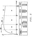
- Fig. 2 shows a chart of configuration windows and efficiency vs. iDAC current. It illustrates how the implementation will look like in respect to an efficiency curve 20 vs. IDAC.
- the table below is a representation of the different configurations. Depending on the resolution required for each variable, a certain number of OTP registers are required. It shows that the efficiency ⁇ has reached between configuration windows W2 and W3 its maximum.
- the boost converter operates in DCM mode.
- the boost converter operates in CCM mode.
- a purpose of the design in the disclosure presented is to maximize efficiency in a region where the boost converter is operating in DCM mode. Therefore, as shown in Fig. 2 , the optimum efficiency is reached in window W2. In this region the switching losses as well as the conduction losses can be relevant at different degrees; hence there is a need to adapt the profile (WLED, NFET power switch, clk) in order to minimize losses.
- a small hysteresis (also user programmable) guarantees smooth transitions between windows during the ramp up/down of the iDAC current (from 0 to 25mA and vice versa) through all the iDAC programming codes.
- the boundaries of the configuration windows W1-W4 are such that the border between Discontinuous and Continuous Conduction Modes (DCM and CCM) would approximately always be in correspondence to one of them.
- VBOOST and FBK voltages as shown in Fig. 1 , are regulated depends on the boost's operating mode.
- the Duty Cycle depends on the load current (assuming no losses) and its expression differs from the one used in CCM; therefore the expression used to estimate the reference voltage VREF to be programmed in order to achieve a certain value of FBK will change.
- FBK f clk , On ⁇ Resistance , Duty Cycle ;
- Duty Cycle DCM f VBAT VBOOST iDAC ;
- Duty Cycle CCM f VBAT VBOOST ;
- the voltage values for the windows selected as e.g. WLED1, WLED2, WLED3, and WLED4 can be identified during characterization at a testing site and stored in the OTP 31, as shown in Fig. 3b .
- Alternatively formulas to estimate the voltage values of WLED (one for DCM and one for CCM) can also be used and follow the equations (7) and (8).
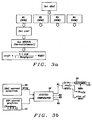
- Fig. 3b shows a block diagram of a digital core 13 selecting a profile of the driver dependent on the different operating windows.
- the digital core 13 comprises a circuit 30 providing as output a digital word prog defining the value of the IDAC current selected.
- the digital word prog comprises information about a tap point for the reference resistor Rref 9, the scale factor for the power switch NFET 5, and the clock frequency of the PWM signal clk.
- the digital programming word "prog" is an N-bit word to define any of the 2 power of N iDAC values between 0 and 25mA decoded in the example of the preferred embodiment in a logarithmic scale.
- the iDAC selection block looks like a look-up table with currents vs. digital codes.
- the digital core 13 comprises an OTP memory 31 containing the profiles of all windows, e.g. in the preferred embodiment the profiles of windows W1-W4. Other numbers of windows are also possible.
- the digital word prog representing the IDAC current selected and the profile of operation windows are input of a digital comparator 32, i.e. the value of the PWM clock frequency clk , the size of the power switch NFET 5, and the resistance of the reference resistor Rref 9. These values are set by the comparator 32 according the operation window selected dependent on the IDAC current selected.
- the frequency clk is set via a programmable digital frequency divider 33 using in the preferred embodiment a base frequency of e.g. 3 MHz. Other base frequencies can be used as well.
- the next Fig. 4a presents the programmable current source IDAC 6 implemented in this system. It is a regulated current source that guarantees a very accurate output current and allows to operate with a very low FBK voltage ( ⁇ 150mV typically for iDAC up to a current of 25mA or higher).
- the circuit of Fig. 4a comprises a reference branch comprising the current source 42, providing constant current, transistor N0 43, transistor switch Nswitch0 44 and transistor N1 45.
- the reference branch generates Vcasc voltage.
- the Nswitch0 44 replicates the voltage drop on the output branch due to the selection switch Nswitch 47.
- the output branch comprises transistor N2 46, transistor Nswitch 47 and output transistor Nout 40.
- the transistor NOUT 40 delivers the output current IDAC.
- Amplifier 41 controls the gate of transistor NOUT 40.
- the amplifier 41 together with transistor NOUT 40 provides a regulation that guarantees voltage Vdac equals voltage Vcasc.
- the size of transistors N1 and N2 is such that the saturation operation is guaranteed for very low drain-source voltages ( ⁇ 150 mV) and is the most important element to achieve efficiency of the boost operation.
- Transistors N2 46 and N1 45 form a current mirror.
- the gate of transistor NSWITCH 47 is controlled by a voltage corresponding to a digital word prog, which is used to select the IDAC current.
- the adjustment of the transistor N2 46 via Nswitch 47 can be performed by e.g. by logarithmic steps or in another sequence.
- N2 devices there are actually a number of N2 devices in parallel, each with an Nswitch device on top.
- a number of Nswitch devices are closed in sequence.
- the non-selected branches are with the Nswitch device open therefore that portion of the N2 device does not take part to the conduction.
- the scaling ratio of the N2 devices is not binary weighted but logarithmic, meaning that for small codes (small currents) the ratio increases at slow rate, while when large codes (large currents) are selected the ratio is larger.
- the size of Nswitch device is proportional to the size of the N2 device underneath.
- Fig. 4b shows a diagram of the output currents IDAC of the programmable current source versus the IDAC output voltage FBK.
- the IDAC values shown are for a maximum case 400 and typical case 401, wherein X2 stands for 2 strings of WLED supported.
- VREF The programming of VREF is explained in Fig. 3a .
- the selection of VREF is linked to the voltage gain (GV) of the Error Amplifier EA 7.
- GV voltage gain
- the GV can be programmed higher or lower to improve load regulation.
- the proposed implementation is done as such that the range of available VREF values can cover for the range of available GV.
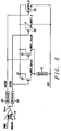
- Fig. 5 depicts the configurable power switch system NFET 5.
- Fig. 5 shows how the power switch system NFET 5 is configured.
- Fig. 5 illustrates the PWM comparator 10, as also shown in Fig. 1 , driving via driver A 54 and via driver B 55 the programmable power switch comprising in the example of Fig. 5 a first part NFET_A 52 and NFET_B 53.
- the table below illustrates how the setting of both drivers 54 and 55 activates gate A or Gate B or both.
- the drivers 54 and 55 are simple buffer stages made of a series of MOS inverters (NFET + PFET) in order to scale up the driving strength and cope with the large capacitive load of gate A and gate B. Obviously the driving strength of driver A and B will be proportional to the gate size that they have to drive. When a gate is OFF, the input of the correspondent driver is set constantly to ground, while when a gate is ON, the correspondent driver is left to switch according to the PWM signal. Dedicated logic is used to prevent the overlapping of the rising and falling edges of the drivers and avoid cross conduction (which will cause loss in efficiency).
- parallel multiple driving stages can be associated to separate NFET devices in order to scale the pull down capability at the LX node in relation to the output current of the boost converter.
- NFET_A the On-Resistance of NFET_A (52) will be 40% higher and the gate to source capacitance, which needs to be charged/discharged at every cycle, to be approximately 40% lower.
- the NFET_A ratio is used for low load configuration where SLoss dominate with respect to CLoss.
- the current sensing (for slope compensation and current limiting) is performed using a scaled version (NFET_SensA 50 and NFET_SensB 51) of the main power switch (hence there is little contribution to the conduction of the boost current from the sense devices), which mirrors the main current into a sense resistor Rsense 12.
- the main point is that if power switch system NFET 5 changes its size according to current iDAC, the mirroring ratio stays constant hence the current gain (for slope compensation) and current limits (to prevent coil saturation) also remain constant.
- the switching frequency clk selection is made through a programmable frequency divider for fine steps tuning (5bits) in the range e.g. between 0.25 and 3MHz.
- fine steps tuning 5bits
- clk is reduced to minimize SLoss; the fine-tuning is needed to optimize the efficiency in respect to NFET and iDAC.
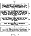
- Fig. 6 illustrates a flowchart of a method disclosed to optimize the efficiency of a boost converter for a white LED driver.
- Step 60 of the method of Fig. 6 illustrates the provision of an arrangement of one or more white LEDs in series, a programmable current source, and a boost converter comprising a size programmable power switch, a PWM generator with programmable clock frequency, and a programmable reference voltage generator for an error amplifier stage.
- Step 61 depicts identifying a number of configuration windows specifying configuration of the WLED driver and mode of modulation, wherein the configuration windows and modulation mode depend on current iDAC required through the WLED arrangement.
- Step 62 illustrates defining clock frequency, size of power switch and said programmable reference voltage once the current iDAC is known.
- Step 63 illustrates storing characteristics of all configuration windows selected.
- Step 64 depicts implementing configuration of a specific WLED driver for a specific WLED arrangement according to the corresponding configuration window providing optimum efficiency in regard of correspondent characteristics.
Landscapes
- Dc-Dc Converters (AREA)
Claims (23)
- Un procédé d'optimisation de l'efficacité d'un pilote LED, comprenant les étapes suivantes :(1) fournir un dispositif comportant une disposition d'une ou plusieurs LEDs (1) en série, une source de courrant iDAC programmable (6), et un convertisseur élévateur (100) comportant un commutateur de puissance de dimension programmable (5), un générateur PWM (10, 11) à fréquence programmable (Clk), et un générateur de potentiel de référence programmable (9) pour un étage amplificateur d'erreur (7) ;(2) identifier un nombre de fenêtres de configuration spécifiant la configuration du pilote de LED et du mode de modulation (61), dans lequel les fenêtres de configuration et le mode de modulation dépendent du courant iDAC requis via la disposition de LED ;(3) définir la fréquence d'horloge, la dimension du commutateur de puissance et ledit potentiel de référence programmable dès lors que le courant iDAC est connu (62) ;(4) le stockage des caractéristiques de toutes les fenêtres de configuration sélectionnées (63) ; et(5) l'implémentation de la configuration d'un pilote LED spécifique pour une disposition LED spécifique en fonction de la fenêtre de configuration correspondante fournissant l'efficacité optimale au regard des caractéristiques correspondantes (64).
- Le procédé de la revendication 1 dans lequel le stockage des caractéristiques de toutes les fenêtres de configuration sélectionnées est effectué durant une phase de réglage du dispositif.
- Le procédé de la revendication 1 dans lequel quatre fenêtres de configuration sont sélectionnées, chacune recouvrant une gamme de courant iDAC.
- le procédé de la revendication 1 dans lequel des frontières des fenêtres de configuration peuvent comporter un bord entre des Modes de Conduction Discontinues ou Continues du convertisseur élevateur (100).
- Le procédé de la revendication 1 dans lequel une courbe représentative de l'efficacité des fenêtres de configuration qui sont fonctions du courant iDAC requis sert de base à la définition des gammes des fenêtres de configuration.
- Le procédé de la revendication 1 dans lequel le courant généré par la source de courant iDAC (6) est programmées par niveaux, par exemple programmée en une séquence logarithmique pour compenser la réponse rétinienne humaine.
- Le procédé de la revendication 1 dans lequel un mot de programmation pour la source de courants iDAC (6) est utilisé pour fixer un point milieu d'une résistance, laquelle définit le potentiel de référence pour l'amplificateur d'erreur (7), un facteur d'échelle pour le commutateur de puissance (5), et la fréquence d'horloge du générateur PWM (10).
- Le procédé de la revendication 1 dans lequel un hystérésis programmable d'utilisateur peut être fixé pour permettre des transitions douces entre des fenêtres durant la montée/descente du courant iDAC.
- Le procédé de la revendication 1 dans lequel la source de courant programmable (6) permet la génération d'un courant avec une tension minimale, e.g. un courant de 25 mA par exemple ou supérieur avec un potentiel égal à environ 150mV ou inférieur.
- Le procédé de la revendication 1 dans lequel une méthode de calcul du potentiel de référence programmable pour l'amplificateur d'erreur (7) comporte les étapes :(1) fixer l'iDAC ainsi que la fenêtre de configuration correspondante ;(2) fixer la fréquence d'horloge correspondant à la fenêtre de configuration sélectionnée ;(3) fixer la dimension du commutateur de puissance (5) correspondant à la fenêtre de configuration sélectionnée et ainsi définir la résistance ON du commutateur de puissance (5), et(4) calculer VREF en fonction de l'équation :

- Le procédé de la revendication 1 dans lequel la détection de courant du commutateur de puissance (5) est effectuée en utilisant une version à l'échelle du commutateur de puissance principal, dans lequel la version à l'échelle effectue un miroir du courant principal au sein d'une résistance de mesure (6).
- Le procédé de la revendication 1, dans lequel le procédé est appliqué pour la commande de LEDs pour des applications lumineuses.
- Un circuit pour un pilote LED ayant une efficacité optimisée, comprenant :- un noyau numérique (13) comprenant :- un bloc de sélection de courant (30) pour sélectionner un courant généré par une source de courant programmable (6);- une mémoire OTP pour le stockage de profils de fenêtres d'opération (31);- un comparateur numérique (32), et- des moyens de division de fréquence (33) ;dans lequel une sortie du bloc numérique comporte un programme de mot numérique fixant une valeur sélectionnée du courant généré par la source de courant programmable, un signal d'horloge pilotant le générateur PWM (10, 11), un potentiel de référence (9) pour une boucle de régulation, et une dimension de commutateur de puissance de dimension programmable (5) du convertisseur élevateur (100) ;- ledit convertisseur élevateur comprenant :- un port pour un potentiel d'entrée ;- une inductance (2) connectée entre une première électrode du port pour le potentiel d'entrée (VBAT) et un noeud LX ;- des moyens de redressement (3) connectés entre le noeud LX et un potentiel de sortie du convertisseur élevateur (100) ;- une capacité (4) connectée entre les ports de sortie du convertisseur élevateur (100);- ledit commutateur de puissance de dimension programmable (5) étant connecté entre le noeud LX et une seconde électrode d'une résistance de mesure (12), dans lequel le commutateur de puissance est commandé par un signal (GATE) de la boucle de régulation (7, 10, 11);- ladite résistance de mesure (12), dans laquelle une seconde électrode de la résistance de mesure est connectée à une seconde électrode dudit port de potentiel d'entrée (VBAT) ;- ledit générateur PWM (10, 11) pilotant via ladite boucle de régulation ledit commutateur de puissance (5), dans lequel le générateur PWM (10, 11), reçoit ledit signal d'horloge (Clk) ;- ladite boucle de régulation pour commander un potentiel de sortie (VBOOST) de ladite source de courant programmable (6) en utilisant ledit potentiel de référence, qui est connecté entre une seconde électrode de ladite source de courant programmable (6) et une porte dudit commutateur de puissance ;- une ou plusieurs LEDs (1) connectées en série dans lesquelles une première électrode de la ou des LEDs (1) est connectée à un premier port de sortie du convertisseur élevateur et une seconde électrode de la ou des LEDs (1) est connectée à la seconde électrode de la source de courant programmable (6) ; et- ladite source de courant programmable (6) pour générer un courant de polarisation à la LED(s), dans lequel une seconde électrode de la source de courant est connectée à la seconde électrode dudit port pour le potentiel d'entrée.
- Le circuit de la revendication 13 dans lequel lesdits moyens de redressements consistent en une diode Schottky (3).
- Le circuit de la revendication 13 dans lequel ledit commutateur de puissance de dimension programmable (5) est un dispositif NFET.
- Le circuit de la revendication 15 dans lequel ledit dispositif NFET comporte :- un premier transistor de puissance (52) connecté entre le noeud LX et VSS , dans lequel sa grille est connectée à un premier signal de grille ;- un second transistor de puissance (52) connecté entre le noeud LX et VSS, dans lequel sa grille est connectée à un second signal de grille ;- un premier transistor de mesure de courant (50) connecté entre le noeud LX et une première électrode d'une résistance de mesure (12), dans lequel sa grille est connectée au premier signal de grille et le premier transistor de mesure de courant (50) est une version en échelle du premier transistor de puissance (52) ;- un second transistor de mesure de courant (51) connecté entre le noeud LX et une première électrode de la résistance de mesure (12), dans lequel sa grille est connectée au second signal de grille et le second transistor de mesure de courant est une version en échelle du second transistor de puissance ; et- ladite résistance de mesure (12) comporte une seconde électrode connectée au potentiel VSS.
- Le circuit de la revendication 13 dans lequel ledit commutateur de puissance (5), ladite source de courant programmable (6), et ladite boucle de régulation sont tous intégrés au sein d'un circuit intégré et/ou ledit noyau numérique est intégré au sein du circuit intégré.
- Le circuit de la revendication 13 dans lequel lesdits LEDs (1) sont des LEDs blanches.
- Le circuit de la revendication 13 dans lequel ladite source de courant programmable (6) comporte :- une branche de référence comprenant :- une source de courant constant (42) connectée à une grille et drain du premier transistor NMOS (43) ;- ledit premier transistor NMOS (43), dans lequel une source et une électrode de profondeur sont connectées à un drain d'un second transistor (44) et à une entrée positive d'un amplificateur (41), et ladite grille est connectée à une grille d'un troisième transistor (45) ;- ledit second transistor (44) ; dans lequel une source est connectée au drain dudit transistor (45) ; une électrode de profondeur est connectée à une électrode de profondeur du troisième transistor (45) et à une source du troisième transistor (45) ; et une grille est connectée au potentiel Vdd ; et- ledit troisième transistor (45) ; dans lequel une grille est connectée à une grille d'un quatrième transistor (46) ; une électrode de profondeur est connectée à une source du troisième transistor (45) et à une source et électrode de profondeur du quatrième transistor (46) ;- une branche de sortie comprenant :- ledit quatrième transistor (46), dans lequel l'électrode de profondeur est connectée à une électrode de profondeur d'un cinquième transistor de programmation de dimension (47) et un drain est connecté à une source du cinquième transistor (47) ;- ledit cinquième transistor (47), dans lequel sa grille est connectée à la sortie dudit noyau numérique (13), recevant le mot numérique fixant une valeur du courant de sortie de la source de courant programmable (6) et un drain est connecté à une entrée négative de l'amplificateur (41) et à une source et une électrode de profondeur d'un transistor de sortie (40) de la source de courant programmable (6), et- ledit transistor de sortie (40), dans lequel son drain fournit le courant de sortie de la source de courant programmable (6) et sa grille est connectée à une sortie dudit amplificateur (41), et- ledit amplificateur (41), dans lequel l'amplificateur et le transistor de sortie (40) fournissent une régulation assurant qu'un niveau de potentiel à l'entrée positive de l'amplificateur est égal à un niveau de potentiel à la source du transistor de sortie (40).
- Le circuit de la revendication 19 dans lequel les dimensions de chacun des troisième (45) et quatrième (46) transistors sont telles qu'une opération de saturation est assurée pour des tensions drain source inférieures à 150 milli volts.
- Le circuit de la revendication 19 dans lequel il y a plus d'un transistors pour ledit quatrième transistor (46) qui sont connectés en parallèle et chacun des transistors (46) ayant, sur le dessus, un transistor du type du cinquième transistor (47).
- Le circuit de la revendication 21 dans lequel, pour accroître le taux de miroir désiré et pour atteindre le niveau de courant désiré, l'on ferme en séquence un nombre de transistors parmi lesdits cinquièmes transistors (47), dans lesquels les quatrième transistors (46) qui ont arrêtés les cinquièmes transistors (47) sur le dessus ne sont pas sélectionnés et ne prennent pas part à la conduction.
- Le circuit de la revendication 13 dans lequel ladite boucle de régulation comporte :- un amplificateur d'erreur (7), dans lequel une entrée négative est connectée à la seconde électrode de la source de courant programmable (6), une entrée positive est une tension de référence (VREF), qui est fixée par un générateur de tension de référence (9) via ledit mot numérique, et la sortie de l'amplificateur d'erreur est connecté à un comparateur PWM (10) ;- ledit comparateur PWM (10), dans lequel une entrée positive est connectée à une sortie d'un générateur d'impulsions PWM (11), par exemple un générateur d'impulsions en dents de scie (11), et une sortie est connectée à la grille du commutateur de puissance (5) ;- ledit générateur d'impulsions PWM (11) ; dans lequel une entrée est une fréquence d'horloge (clk), qui est fixée via un diviseur de fréquence réglé par ledit mot numérique ; et- ledit générateur de tension de référence (9) comprenant une source de courant (8) ayant une première électrode connectée à l'entrée positive de l'amplificateur d'erreur et à une première électrode d'une résistance programmable (9) ; dans lequel une seconde électrode de la résistance programmable (9) est connectée à la tension VSS, et dans lequel ledit mot numérique fixe un échelon de la résistance programmable (9) pour sélectionner le potentiel de référence (VREF).
Priority Applications (2)
| Application Number | Priority Date | Filing Date | Title |
|---|---|---|---|
| EP12002094.6A EP2642823B1 (fr) | 2012-03-24 | 2012-03-24 | Procédé pour optimiser l'efficacité par rapport au courant de charge dans un convertisseur survolteur inductif de pilotage de DEL blanche |
| US13/441,070 US8624511B2 (en) | 2012-03-24 | 2012-04-06 | Method for optimizing efficiency versus load current in an inductive boost converter for white LED driving |
Applications Claiming Priority (1)
| Application Number | Priority Date | Filing Date | Title |
|---|---|---|---|
| EP12002094.6A EP2642823B1 (fr) | 2012-03-24 | 2012-03-24 | Procédé pour optimiser l'efficacité par rapport au courant de charge dans un convertisseur survolteur inductif de pilotage de DEL blanche |
Publications (2)
| Publication Number | Publication Date |
|---|---|
| EP2642823A1 EP2642823A1 (fr) | 2013-09-25 |
| EP2642823B1 true EP2642823B1 (fr) | 2016-06-15 |
Family
ID=45999525
Family Applications (1)
| Application Number | Title | Priority Date | Filing Date |
|---|---|---|---|
| EP12002094.6A Active EP2642823B1 (fr) | 2012-03-24 | 2012-03-24 | Procédé pour optimiser l'efficacité par rapport au courant de charge dans un convertisseur survolteur inductif de pilotage de DEL blanche |
Country Status (2)
| Country | Link |
|---|---|
| US (1) | US8624511B2 (fr) |
| EP (1) | EP2642823B1 (fr) |
Families Citing this family (21)
| Publication number | Priority date | Publication date | Assignee | Title |
|---|---|---|---|---|
| CN102780395B (zh) * | 2012-07-09 | 2015-03-11 | 昂宝电子(上海)有限公司 | 用于增强电源变换系统的动态响应的系统和方法 |
| US9523724B2 (en) * | 2013-04-05 | 2016-12-20 | Texas Instruments Incorporated | Tracking energy consumption using a boost technique |
| US9231476B2 (en) | 2013-05-01 | 2016-01-05 | Texas Instruments Incorporated | Tracking energy consumption using a boost-buck technique |
| EP2894944A1 (fr) * | 2014-01-14 | 2015-07-15 | Dialog Semiconductor GmbH | Procédé permettant d'améliorer la précision d'un convertisseur numérique-analogique (IDAC) exponentiel utilisant un MSB à pondération binaire |
| EP2894943B1 (fr) | 2014-01-14 | 2020-02-26 | Dialog Semiconductor (UK) Limited | Appareil permettant d'améliorer la précision d'un convertisseur numérique-analogique (IDAC) exponentiel utilisant un MSB à pondération binaire |
| DE102014219840B4 (de) | 2014-09-30 | 2016-11-03 | Dialog Semiconductor (Uk) Limited | Stromgenerator und Verfahren mit geringem Overhead für Beleuchtungsschaltungen |
| CN104883780B (zh) * | 2015-05-19 | 2017-06-23 | 深圳创维-Rgb电子有限公司 | 多通道双模式数字控制led驱动电路及led灯 |
| KR102529171B1 (ko) * | 2016-02-26 | 2023-05-04 | 삼성전자주식회사 | 메모리 장치 진단 시스템 |
| CN107295713B (zh) * | 2016-03-31 | 2019-08-02 | 青岛海信电器股份有限公司 | 终端设备及其控制方法 |
| CN107333353A (zh) * | 2017-06-30 | 2017-11-07 | 金陵科技学院 | 一种集成化高可靠性高压led发光灯珠及芯片及发光装置 |
| US10014848B1 (en) | 2017-08-25 | 2018-07-03 | Elite Semiconductor Memory Technology Inc. | Compensation circuit for input voltage offset of error amplifier and error amplifier circuit |
| US10422818B2 (en) * | 2017-12-30 | 2019-09-24 | Texas Instruments Incorporated | Power transistors with a resistor coupled to a sense transistor |
| EP3776793A1 (fr) | 2018-04-06 | 2021-02-17 | Signify Holding B.V. | Système doté d'une batterie et son procédé de commande |
| DE102019100058A1 (de) * | 2019-01-03 | 2020-07-09 | Tridonic Gmbh & Co Kg | Beleuchtungssystem mit Energiespar-Modus und Verfahren zur Optimierung der Gesamteffizienz des Beleuchtungssystems |
| WO2020183972A1 (fr) * | 2019-03-11 | 2020-09-17 | 富士電機株式会社 | Circuit intégré et circuit d'alimentation électrique |
| US11327514B2 (en) | 2020-03-26 | 2022-05-10 | Stmicroelectronics (Grenoble 2) Sas | Device for providing a current |
| TWI748518B (zh) * | 2020-06-15 | 2021-12-01 | 瑞昱半導體股份有限公司 | 光接收器裝置、脈波寬度調變器電路系統與靈敏度控制方法 |
| CN113824319B (zh) * | 2020-06-19 | 2025-03-04 | 瑞昱半导体股份有限公司 | 光接收器装置、脉冲宽度调制器电路系统与灵敏度控制方法 |
| CN113433839B (zh) * | 2021-06-28 | 2022-07-01 | 杭州电子科技大学 | 一种基于虚拟电感和虚拟电容的同步整流Boost变换器仿真电路 |
| TWI832742B (zh) * | 2023-03-31 | 2024-02-11 | 宏碁股份有限公司 | 抑制磁飽和之升壓轉換器 |
| US20250155958A1 (en) * | 2023-11-15 | 2025-05-15 | Texas Instruments Incorporated | Methods and apparatus for power saving mode |
Family Cites Families (23)
| Publication number | Priority date | Publication date | Assignee | Title |
|---|---|---|---|---|
| US6963178B1 (en) * | 1998-12-07 | 2005-11-08 | Systel Development And Industries Ltd. | Apparatus for controlling operation of gas discharge devices |
| JP2005284710A (ja) | 2004-03-30 | 2005-10-13 | Sanyo Electric Co Ltd | 駆動回路 |
| US7205920B2 (en) * | 2004-09-17 | 2007-04-17 | Analog Devices, Inc. | Continuous-time-sigma-delta DAC using chopper stabalization |
| US7187136B2 (en) * | 2004-10-25 | 2007-03-06 | Osram Sylvania, Inc. | Method and circuit for regulating power in a high intensity discharge lamp |
| US20080001547A1 (en) * | 2005-09-20 | 2008-01-03 | Negru Sorin L | Driving parallel strings of series connected LEDs |
| US7236046B2 (en) | 2005-11-01 | 2007-06-26 | Catalyst Semiconductor, Inc. | LED bias current control using adaptive fractional charge pump |
| US20080068066A1 (en) | 2006-09-18 | 2008-03-20 | Netasic Llc | High efficiency white LED drivers |
| US7579786B2 (en) * | 2007-06-04 | 2009-08-25 | Applied Concepts, Inc. | Method, apparatus, and system for driving LED's |
| US8373346B2 (en) * | 2007-08-06 | 2013-02-12 | Nxp B.V. | Solid state lighting system and a driver integrated circuit for driving light emitting semiconductor devices |
| US7893674B2 (en) * | 2007-09-26 | 2011-02-22 | Qualcomm, Incorporated | Switch mode power supply (SMPS) and methods thereof |
| US20100207536A1 (en) * | 2007-10-26 | 2010-08-19 | Lighting Science Group Corporation | High efficiency light source with integrated ballast |
| DE102007057230A1 (de) * | 2007-11-28 | 2009-06-04 | Kostal Industrie Elektrik Gmbh | Verfahren zur Steuerung eines Gleichstromstellers |
| US8040070B2 (en) * | 2008-01-23 | 2011-10-18 | Cree, Inc. | Frequency converted dimming signal generation |
| US8049439B2 (en) * | 2009-01-30 | 2011-11-01 | Freescale Semiconductor, Inc. | LED driver with dynamic headroom control |
| US8310171B2 (en) * | 2009-03-13 | 2012-11-13 | Led Specialists Inc. | Line voltage dimmable constant current LED driver |
| US7889525B2 (en) * | 2009-03-25 | 2011-02-15 | Intersil Americas Inc. | System and method for phase dropping and adding |
| TWI495393B (zh) * | 2009-05-09 | 2015-08-01 | Innosys Inc | 通用型調光器 |
| WO2010137202A1 (fr) * | 2009-05-28 | 2010-12-02 | シャープ株式会社 | Dispositif d'attaque de del, dispositif source de lumière, et dispositif d'affichage à cristaux liquides |
| WO2011002280A1 (fr) * | 2009-06-30 | 2011-01-06 | Eldolab Holding B.V. | Procédé de configuration de circuit de commande de led, circuit de commande de led, assemblage de led et procédé de contrôle d'un assemblage de led |
| WO2011021075A1 (fr) * | 2009-08-18 | 2011-02-24 | Freescale Semiconductor, Inc. | Système de commande, circuit intégré et leur procédé |
| TW201212704A (en) * | 2010-09-13 | 2012-03-16 | Leadtrend Tech Corp | Driving integrated circuit of a light emitting diode |
| US8779686B2 (en) * | 2010-10-24 | 2014-07-15 | Microsemi Corporation | Synchronous regulation for LED string driver |
| US8773031B2 (en) * | 2010-11-22 | 2014-07-08 | Innosys, Inc. | Dimmable timer-based LED power supply |
-
2012
- 2012-03-24 EP EP12002094.6A patent/EP2642823B1/fr active Active
- 2012-04-06 US US13/441,070 patent/US8624511B2/en active Active
Also Published As
| Publication number | Publication date |
|---|---|
| US8624511B2 (en) | 2014-01-07 |
| US20130249421A1 (en) | 2013-09-26 |
| EP2642823A1 (fr) | 2013-09-25 |
Similar Documents
| Publication | Publication Date | Title |
|---|---|---|
| EP2642823B1 (fr) | Procédé pour optimiser l'efficacité par rapport au courant de charge dans un convertisseur survolteur inductif de pilotage de DEL blanche | |
| US7307614B2 (en) | Light emitting diode driver circuit | |
| US7812647B2 (en) | MOSFET gate drive with reduced power loss | |
| JP5205974B2 (ja) | 直流電源装置、led駆動用電源装置および電源制御用半導体集積回路 | |
| EP2852258B1 (fr) | Dispositif de commande de source de lumière | |
| US7724219B2 (en) | Circuit and method of effectively enhancing drive control of light-emitting diodes | |
| US8288953B1 (en) | Buck constant average current regulation of light emitting diodes | |
| US20080180039A1 (en) | Led drive circuit | |
| US9058050B2 (en) | Clock-based soft-start circuit and power management integrated circuit device | |
| US7915878B2 (en) | Switching regulator and method of converting DC voltage | |
| US20170055322A1 (en) | Driver circuit with extended operation range | |
| US10468982B2 (en) | Switching power supply circuit, load driving device, and liquid crystal display device | |
| EP2079157A2 (fr) | Dispositif d'alimentation électrique en courant continu, dispositif d'alimentation électrique pour DEL et circuit intégré semi-conducteur pour la commande de l'alimentation électrique | |
| CN110619853B (zh) | 具有电流匹配的功率转换器 | |
| US7151361B2 (en) | Current sensing circuitry for DC-DC converters | |
| US20120098514A1 (en) | Current mode switching regulator and control circuit and control method thereof | |
| US20100001702A1 (en) | Single pin multi-vid bit interface circuit for dynamic voltage change of a dc/dc converter | |
| US20120081091A1 (en) | Control circuit, dcdc converter, and driving method | |
| US9787183B2 (en) | Driver and driving control method for power converter | |
| CN107431427A (zh) | 在组合开关与线性调节器中使用pmos电源开关 | |
| US8860330B1 (en) | Programmable current source with optimized compliance region for efficient backlighting in portable applications | |
| US9622305B2 (en) | WLED driver and drive control method | |
| TWI408542B (zh) | 用於供應電源的設備 | |
| KR101014998B1 (ko) | 멀티 채널 스텝 업 직류 직류 컨버터 | |
| JP2006033974A (ja) | 電源回路 |
Legal Events
| Date | Code | Title | Description |
|---|---|---|---|
| PUAI | Public reference made under article 153(3) epc to a published international application that has entered the european phase |
Free format text: ORIGINAL CODE: 0009012 |
|
| AK | Designated contracting states |
Kind code of ref document: A1 Designated state(s): AL AT BE BG CH CY CZ DE DK EE ES FI FR GB GR HR HU IE IS IT LI LT LU LV MC MK MT NL NO PL PT RO RS SE SI SK SM TR |
|
| AX | Request for extension of the european patent |
Extension state: BA ME |
|
| 17P | Request for examination filed |
Effective date: 20140321 |
|
| RBV | Designated contracting states (corrected) |
Designated state(s): AL AT BE BG CH CY CZ DE DK EE ES FI FR GB GR HR HU IE IS IT LI LT LU LV MC MK MT NL NO PL PT RO RS SE SI SK SM TR |
|
| GRAP | Despatch of communication of intention to grant a patent |
Free format text: ORIGINAL CODE: EPIDOSNIGR1 |
|
| INTG | Intention to grant announced |
Effective date: 20151222 |
|
| GRAS | Grant fee paid |
Free format text: ORIGINAL CODE: EPIDOSNIGR3 |
|
| GRAA | (expected) grant |
Free format text: ORIGINAL CODE: 0009210 |
|
| AK | Designated contracting states |
Kind code of ref document: B1 Designated state(s): AL AT BE BG CH CY CZ DE DK EE ES FI FR GB GR HR HU IE IS IT LI LT LU LV MC MK MT NL NO PL PT RO RS SE SI SK SM TR |
|
| REG | Reference to a national code |
Ref country code: CH Ref legal event code: EP Ref country code: GB Ref legal event code: FG4D |
|
| REG | Reference to a national code |
Ref country code: IE Ref legal event code: FG4D |
|
| REG | Reference to a national code |
Ref country code: AT Ref legal event code: REF Ref document number: 807076 Country of ref document: AT Kind code of ref document: T Effective date: 20160715 |
|
| REG | Reference to a national code |
Ref country code: DE Ref legal event code: R096 Ref document number: 602012019506 Country of ref document: DE |
|
| REG | Reference to a national code |
Ref country code: LT Ref legal event code: MG4D |
|
| REG | Reference to a national code |
Ref country code: NL Ref legal event code: MP Effective date: 20160615 |
|
| PG25 | Lapsed in a contracting state [announced via postgrant information from national office to epo] |
Ref country code: NO Free format text: LAPSE BECAUSE OF FAILURE TO SUBMIT A TRANSLATION OF THE DESCRIPTION OR TO PAY THE FEE WITHIN THE PRESCRIBED TIME-LIMIT Effective date: 20160915 Ref country code: FI Free format text: LAPSE BECAUSE OF FAILURE TO SUBMIT A TRANSLATION OF THE DESCRIPTION OR TO PAY THE FEE WITHIN THE PRESCRIBED TIME-LIMIT Effective date: 20160615 Ref country code: LT Free format text: LAPSE BECAUSE OF FAILURE TO SUBMIT A TRANSLATION OF THE DESCRIPTION OR TO PAY THE FEE WITHIN THE PRESCRIBED TIME-LIMIT Effective date: 20160615 |
|
| REG | Reference to a national code |
Ref country code: AT Ref legal event code: MK05 Ref document number: 807076 Country of ref document: AT Kind code of ref document: T Effective date: 20160615 |
|
| PG25 | Lapsed in a contracting state [announced via postgrant information from national office to epo] |
Ref country code: GR Free format text: LAPSE BECAUSE OF FAILURE TO SUBMIT A TRANSLATION OF THE DESCRIPTION OR TO PAY THE FEE WITHIN THE PRESCRIBED TIME-LIMIT Effective date: 20160916 Ref country code: NL Free format text: LAPSE BECAUSE OF FAILURE TO SUBMIT A TRANSLATION OF THE DESCRIPTION OR TO PAY THE FEE WITHIN THE PRESCRIBED TIME-LIMIT Effective date: 20160615 Ref country code: SE Free format text: LAPSE BECAUSE OF FAILURE TO SUBMIT A TRANSLATION OF THE DESCRIPTION OR TO PAY THE FEE WITHIN THE PRESCRIBED TIME-LIMIT Effective date: 20160615 Ref country code: RS Free format text: LAPSE BECAUSE OF FAILURE TO SUBMIT A TRANSLATION OF THE DESCRIPTION OR TO PAY THE FEE WITHIN THE PRESCRIBED TIME-LIMIT Effective date: 20160615 Ref country code: LV Free format text: LAPSE BECAUSE OF FAILURE TO SUBMIT A TRANSLATION OF THE DESCRIPTION OR TO PAY THE FEE WITHIN THE PRESCRIBED TIME-LIMIT Effective date: 20160615 |
|
| PG25 | Lapsed in a contracting state [announced via postgrant information from national office to epo] |
Ref country code: EE Free format text: LAPSE BECAUSE OF FAILURE TO SUBMIT A TRANSLATION OF THE DESCRIPTION OR TO PAY THE FEE WITHIN THE PRESCRIBED TIME-LIMIT Effective date: 20160615 Ref country code: IT Free format text: LAPSE BECAUSE OF FAILURE TO SUBMIT A TRANSLATION OF THE DESCRIPTION OR TO PAY THE FEE WITHIN THE PRESCRIBED TIME-LIMIT Effective date: 20160615 Ref country code: SK Free format text: LAPSE BECAUSE OF FAILURE TO SUBMIT A TRANSLATION OF THE DESCRIPTION OR TO PAY THE FEE WITHIN THE PRESCRIBED TIME-LIMIT Effective date: 20160615 Ref country code: IS Free format text: LAPSE BECAUSE OF FAILURE TO SUBMIT A TRANSLATION OF THE DESCRIPTION OR TO PAY THE FEE WITHIN THE PRESCRIBED TIME-LIMIT Effective date: 20161015 Ref country code: RO Free format text: LAPSE BECAUSE OF FAILURE TO SUBMIT A TRANSLATION OF THE DESCRIPTION OR TO PAY THE FEE WITHIN THE PRESCRIBED TIME-LIMIT Effective date: 20160615 Ref country code: CZ Free format text: LAPSE BECAUSE OF FAILURE TO SUBMIT A TRANSLATION OF THE DESCRIPTION OR TO PAY THE FEE WITHIN THE PRESCRIBED TIME-LIMIT Effective date: 20160615 |
|
| PG25 | Lapsed in a contracting state [announced via postgrant information from national office to epo] |
Ref country code: SM Free format text: LAPSE BECAUSE OF FAILURE TO SUBMIT A TRANSLATION OF THE DESCRIPTION OR TO PAY THE FEE WITHIN THE PRESCRIBED TIME-LIMIT Effective date: 20160615 Ref country code: PL Free format text: LAPSE BECAUSE OF FAILURE TO SUBMIT A TRANSLATION OF THE DESCRIPTION OR TO PAY THE FEE WITHIN THE PRESCRIBED TIME-LIMIT Effective date: 20160615 Ref country code: BE Free format text: LAPSE BECAUSE OF FAILURE TO SUBMIT A TRANSLATION OF THE DESCRIPTION OR TO PAY THE FEE WITHIN THE PRESCRIBED TIME-LIMIT Effective date: 20160615 Ref country code: AT Free format text: LAPSE BECAUSE OF FAILURE TO SUBMIT A TRANSLATION OF THE DESCRIPTION OR TO PAY THE FEE WITHIN THE PRESCRIBED TIME-LIMIT Effective date: 20160615 Ref country code: PT Free format text: LAPSE BECAUSE OF FAILURE TO SUBMIT A TRANSLATION OF THE DESCRIPTION OR TO PAY THE FEE WITHIN THE PRESCRIBED TIME-LIMIT Effective date: 20161017 Ref country code: ES Free format text: LAPSE BECAUSE OF FAILURE TO SUBMIT A TRANSLATION OF THE DESCRIPTION OR TO PAY THE FEE WITHIN THE PRESCRIBED TIME-LIMIT Effective date: 20160615 |
|
| REG | Reference to a national code |
Ref country code: DE Ref legal event code: R097 Ref document number: 602012019506 Country of ref document: DE |
|
| PLBE | No opposition filed within time limit |
Free format text: ORIGINAL CODE: 0009261 |
|
| STAA | Information on the status of an ep patent application or granted ep patent |
Free format text: STATUS: NO OPPOSITION FILED WITHIN TIME LIMIT |
|
| 26N | No opposition filed |
Effective date: 20170316 |
|
| PG25 | Lapsed in a contracting state [announced via postgrant information from national office to epo] |
Ref country code: DK Free format text: LAPSE BECAUSE OF FAILURE TO SUBMIT A TRANSLATION OF THE DESCRIPTION OR TO PAY THE FEE WITHIN THE PRESCRIBED TIME-LIMIT Effective date: 20160615 |
|
| PG25 | Lapsed in a contracting state [announced via postgrant information from national office to epo] |
Ref country code: SI Free format text: LAPSE BECAUSE OF FAILURE TO SUBMIT A TRANSLATION OF THE DESCRIPTION OR TO PAY THE FEE WITHIN THE PRESCRIBED TIME-LIMIT Effective date: 20160615 |
|
| REG | Reference to a national code |
Ref country code: CH Ref legal event code: PL |
|
| PG25 | Lapsed in a contracting state [announced via postgrant information from national office to epo] |
Ref country code: MC Free format text: LAPSE BECAUSE OF FAILURE TO SUBMIT A TRANSLATION OF THE DESCRIPTION OR TO PAY THE FEE WITHIN THE PRESCRIBED TIME-LIMIT Effective date: 20160615 |
|
| REG | Reference to a national code |
Ref country code: IE Ref legal event code: MM4A |
|
| REG | Reference to a national code |
Ref country code: FR Ref legal event code: ST Effective date: 20171130 |
|
| PG25 | Lapsed in a contracting state [announced via postgrant information from national office to epo] |
Ref country code: LU Free format text: LAPSE BECAUSE OF NON-PAYMENT OF DUE FEES Effective date: 20170324 Ref country code: FR Free format text: LAPSE BECAUSE OF NON-PAYMENT OF DUE FEES Effective date: 20170331 |
|
| PG25 | Lapsed in a contracting state [announced via postgrant information from national office to epo] |
Ref country code: IE Free format text: LAPSE BECAUSE OF NON-PAYMENT OF DUE FEES Effective date: 20170324 Ref country code: LI Free format text: LAPSE BECAUSE OF NON-PAYMENT OF DUE FEES Effective date: 20170331 Ref country code: CH Free format text: LAPSE BECAUSE OF NON-PAYMENT OF DUE FEES Effective date: 20170331 |
|
| PG25 | Lapsed in a contracting state [announced via postgrant information from national office to epo] |
Ref country code: MT Free format text: LAPSE BECAUSE OF NON-PAYMENT OF DUE FEES Effective date: 20170324 |
|
| PG25 | Lapsed in a contracting state [announced via postgrant information from national office to epo] |
Ref country code: AL Free format text: LAPSE BECAUSE OF FAILURE TO SUBMIT A TRANSLATION OF THE DESCRIPTION OR TO PAY THE FEE WITHIN THE PRESCRIBED TIME-LIMIT Effective date: 20160615 |
|
| PG25 | Lapsed in a contracting state [announced via postgrant information from national office to epo] |
Ref country code: HU Free format text: LAPSE BECAUSE OF FAILURE TO SUBMIT A TRANSLATION OF THE DESCRIPTION OR TO PAY THE FEE WITHIN THE PRESCRIBED TIME-LIMIT; INVALID AB INITIO Effective date: 20120324 |
|
| PG25 | Lapsed in a contracting state [announced via postgrant information from national office to epo] |
Ref country code: BG Free format text: LAPSE BECAUSE OF FAILURE TO SUBMIT A TRANSLATION OF THE DESCRIPTION OR TO PAY THE FEE WITHIN THE PRESCRIBED TIME-LIMIT Effective date: 20160615 |
|
| PG25 | Lapsed in a contracting state [announced via postgrant information from national office to epo] |
Ref country code: CY Free format text: LAPSE BECAUSE OF NON-PAYMENT OF DUE FEES Effective date: 20160615 |
|
| REG | Reference to a national code |
Ref country code: DE Ref legal event code: R079 Ref document number: 602012019506 Country of ref document: DE Free format text: PREVIOUS MAIN CLASS: H05B0033080000 Ipc: H05B0045000000 |
|
| PG25 | Lapsed in a contracting state [announced via postgrant information from national office to epo] |
Ref country code: MK Free format text: LAPSE BECAUSE OF FAILURE TO SUBMIT A TRANSLATION OF THE DESCRIPTION OR TO PAY THE FEE WITHIN THE PRESCRIBED TIME-LIMIT Effective date: 20160615 |
|
| PG25 | Lapsed in a contracting state [announced via postgrant information from national office to epo] |
Ref country code: TR Free format text: LAPSE BECAUSE OF FAILURE TO SUBMIT A TRANSLATION OF THE DESCRIPTION OR TO PAY THE FEE WITHIN THE PRESCRIBED TIME-LIMIT Effective date: 20160615 |
|
| PG25 | Lapsed in a contracting state [announced via postgrant information from national office to epo] |
Ref country code: HR Free format text: LAPSE BECAUSE OF FAILURE TO SUBMIT A TRANSLATION OF THE DESCRIPTION OR TO PAY THE FEE WITHIN THE PRESCRIBED TIME-LIMIT Effective date: 20160615 |
|
| REG | Reference to a national code |
Ref country code: DE Ref legal event code: R082 Ref document number: 602012019506 Country of ref document: DE |
|
| PGFP | Annual fee paid to national office [announced via postgrant information from national office to epo] |
Ref country code: GB Payment date: 20260310 Year of fee payment: 15 |
|
| PGFP | Annual fee paid to national office [announced via postgrant information from national office to epo] |
Ref country code: DE Payment date: 20260304 Year of fee payment: 15 |