EP2642834A2 - Carte de circuit imprimé - Google Patents
Carte de circuit imprimé Download PDFInfo
- Publication number
- EP2642834A2 EP2642834A2 EP12165415.6A EP12165415A EP2642834A2 EP 2642834 A2 EP2642834 A2 EP 2642834A2 EP 12165415 A EP12165415 A EP 12165415A EP 2642834 A2 EP2642834 A2 EP 2642834A2
- Authority
- EP
- European Patent Office
- Prior art keywords
- printed circuit
- circuit board
- insulating layer
- conductive metal
- metal layer
- Prior art date
- Legal status (The legal status is an assumption and is not a legal conclusion. Google has not performed a legal analysis and makes no representation as to the accuracy of the status listed.)
- Withdrawn
Links
- 239000002184 metal Substances 0.000 claims abstract description 16
- 229910052751 metal Inorganic materials 0.000 claims abstract description 16
- RYGMFSIKBFXOCR-UHFFFAOYSA-N Copper Chemical compound [Cu] RYGMFSIKBFXOCR-UHFFFAOYSA-N 0.000 claims description 8
- 239000011889 copper foil Substances 0.000 claims description 8
- 238000007599 discharging Methods 0.000 description 5
- 239000004020 conductor Substances 0.000 description 3
- 238000010586 diagram Methods 0.000 description 3
- 238000000034 method Methods 0.000 description 2
- 238000012986 modification Methods 0.000 description 2
- 230000004048 modification Effects 0.000 description 2
- 238000005476 soldering Methods 0.000 description 1
Images

Classifications
-
- H—ELECTRICITY
- H05—ELECTRIC TECHNIQUES NOT OTHERWISE PROVIDED FOR
- H05K—PRINTED CIRCUITS; CASINGS OR CONSTRUCTIONAL DETAILS OF ELECTRIC APPARATUS; MANUFACTURE OF ASSEMBLAGES OF ELECTRICAL COMPONENTS
- H05K1/00—Printed circuits
- H05K1/02—Details
- H05K1/0213—Electrical arrangements not otherwise provided for
- H05K1/0216—Reduction of cross-talk, noise or electromagnetic interference
- H05K1/0218—Reduction of cross-talk, noise or electromagnetic interference by printed shielding conductors, ground planes or power plane
- H05K1/0224—Patterned shielding planes, ground planes or power planes
- H05K1/0225—Single or multiple openings in a shielding, ground or power plane
-
- H—ELECTRICITY
- H05—ELECTRIC TECHNIQUES NOT OTHERWISE PROVIDED FOR
- H05K—PRINTED CIRCUITS; CASINGS OR CONSTRUCTIONAL DETAILS OF ELECTRIC APPARATUS; MANUFACTURE OF ASSEMBLAGES OF ELECTRICAL COMPONENTS
- H05K1/00—Printed circuits
- H05K1/02—Details
- H05K1/0213—Electrical arrangements not otherwise provided for
- H05K1/0216—Reduction of cross-talk, noise or electromagnetic interference
- H05K1/023—Reduction of cross-talk, noise or electromagnetic interference using auxiliary mounted passive components or auxiliary substances
- H05K1/0233—Filters, inductors or a magnetic substance
-
- H—ELECTRICITY
- H05—ELECTRIC TECHNIQUES NOT OTHERWISE PROVIDED FOR
- H05K—PRINTED CIRCUITS; CASINGS OR CONSTRUCTIONAL DETAILS OF ELECTRIC APPARATUS; MANUFACTURE OF ASSEMBLAGES OF ELECTRICAL COMPONENTS
- H05K2201/00—Indexing scheme relating to printed circuits covered by H05K1/00
- H05K2201/10—Details of components or other objects attached to or integrated in a printed circuit board
- H05K2201/10007—Types of components
- H05K2201/1003—Non-printed inductor
-
- H—ELECTRICITY
- H05—ELECTRIC TECHNIQUES NOT OTHERWISE PROVIDED FOR
- H05K—PRINTED CIRCUITS; CASINGS OR CONSTRUCTIONAL DETAILS OF ELECTRIC APPARATUS; MANUFACTURE OF ASSEMBLAGES OF ELECTRICAL COMPONENTS
- H05K2201/00—Indexing scheme relating to printed circuits covered by H05K1/00
- H05K2201/10—Details of components or other objects attached to or integrated in a printed circuit board
- H05K2201/10613—Details of electrical connections of non-printed components, e.g. special leads
- H05K2201/10621—Components characterised by their electrical contacts
- H05K2201/10636—Leadless chip, e.g. chip capacitor or resistor
-
- Y—GENERAL TAGGING OF NEW TECHNOLOGICAL DEVELOPMENTS; GENERAL TAGGING OF CROSS-SECTIONAL TECHNOLOGIES SPANNING OVER SEVERAL SECTIONS OF THE IPC; TECHNICAL SUBJECTS COVERED BY FORMER USPC CROSS-REFERENCE ART COLLECTIONS [XRACs] AND DIGESTS
- Y02—TECHNOLOGIES OR APPLICATIONS FOR MITIGATION OR ADAPTATION AGAINST CLIMATE CHANGE
- Y02P—CLIMATE CHANGE MITIGATION TECHNOLOGIES IN THE PRODUCTION OR PROCESSING OF GOODS
- Y02P70/00—Climate change mitigation technologies in the production process for final industrial or consumer products
- Y02P70/50—Manufacturing or production processes characterised by the final manufactured product
Definitions
- the present disclosure relates to layout structures of printed circuit boards and, particularly, to a layout structure of a printed circuit board capable of reducing electromagnetic interference.
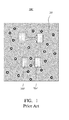
- a printed circuit board 100' of an electronic device such as a Digital Versatile Disc (DVD) player, includes a power switch circuit (not shown) used for repeatedly charging and discharging.
- a copper foil (shown as the shadow) 20' laid on the entire printed circuit board 100' is connected to a ground of the printed circuit board 100', to form a high current ground loop, which is capable of reducing the electromagnetic interference generated in the printed circuit board 100'.
- Most electronic components in the printed circuit board 100' such as a Power Management IC, include a ground pin to form a ground loop, and then connect to the high current ground loop formed by the copper foil 20' via the ground pin, thus eliminating or reducing the electromagnetic interference generated therein.
- an inductor used for repeatedly charging and discharging included in the power switch circuit and connected to the printed circuit board 100' by pads 303' and 304' does not include a ground pin. Thereby, the high-order harmonic distortion and noise generated by the inductor during the process of repeatedly charging and discharging can only be reduced or eliminated by the copper foil covered by the inductor.
- a printed circuit board includes an insulating layer, a conductive metal layer, two pads and an inductor.
- the conductive metal layer is attached on the insulating layer and is grounded, which is configured for providing grounding for electronic components mounted on the printed circuit board.
- the insulating layer includes an exposed portion free of the conductive metal layer thereon, and the two pads are formed on the exposed portion of the insulating layer and are insulated from each other.
- the inductor is mounted on the exposed portion and is electrically connected to the two pads. Thereby a spread path of electromagnetic interference generated by the inductor is cut off, and the interference of the electromagnetic interference to the other electronic components can be effectively reduced.
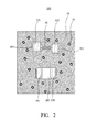
- FIG. 2 is a layout structure of a printed circuit board 100 capable of reducing electromagnetic interference employed in an electronic device (such as DVD player).
- the printed circuit board 100 includes an insulating layer, a conductive metal layer (shown as the shadow) 20, a number of pads, such as pads 301 ⁇ 304 for soldering connecting electronic components, and a number of printed conductors 40 for connecting electronic components.
- the printed board 100 in FIG. 2 only shows a portion of the layout structure of a power switch circuit of the electronic device.
- the conductive metal layer 20 is attached on the insulating layer, and is connected to an internal ground of the printed circuit board 100 for providing grounding for electronic components mounted on the printed circuit board 100.
- the conductive metal layer 20 is a grounded copper foil attached on the insulating layer and is for absorbing the electromagnetic interference generated in the printed circuit board 100.
- the insulating layer includes a number of exposed portions 601 ⁇ 603 free of the conductive metal layer thereon, and pads 301 ⁇ 304 and the printed conductors 40 are formed on the exposed portions of the insulating layer and are insulated from each other.
- the conductive metal layer 20 is separated from the pads 301 ⁇ 304 and the printed conductors 40 to avoid the case of short-circuit.
- a number of grounding holes 50 connected to the internal ground of the printed circuit board 100 are arranged in the conductive metal layer 20 for radiating heat energy and providing space for thermal expansion.
- the power switch circuit includes an inductor 70 for charging and discharging repeatedly.
- the inductor 70 is a chip inductor and is connected to the power switch circuit by being mounted on the exposed portion 603 and being electrically connected to the two pads 303 and 304.
- the two pads 303 and 304 are insulated from each other and no copper foil 20 covers a predetermined range of area between the two pads 303 and 304.
Landscapes
- Physics & Mathematics (AREA)
- Electromagnetism (AREA)
- Engineering & Computer Science (AREA)
- Microelectronics & Electronic Packaging (AREA)
- Structure Of Printed Boards (AREA)
- Shielding Devices Or Components To Electric Or Magnetic Fields (AREA)
- Parts Printed On Printed Circuit Boards (AREA)
Applications Claiming Priority (1)
| Application Number | Priority Date | Filing Date | Title |
|---|---|---|---|
| CN2012100713599A CN103327726A (zh) | 2012-03-19 | 2012-03-19 | 电子装置及其印刷电路板的布局结构 |
Publications (2)
| Publication Number | Publication Date |
|---|---|
| EP2642834A2 true EP2642834A2 (fr) | 2013-09-25 |
| EP2642834A3 EP2642834A3 (fr) | 2014-04-09 |
Family
ID=46025541
Family Applications (1)
| Application Number | Title | Priority Date | Filing Date |
|---|---|---|---|
| EP12165415.6A Withdrawn EP2642834A3 (fr) | 2012-03-19 | 2012-04-24 | Carte de circuit imprimé |
Country Status (5)
| Country | Link |
|---|---|
| US (1) | US20130242519A1 (fr) |
| EP (1) | EP2642834A3 (fr) |
| JP (1) | JP2013197592A (fr) |
| CN (1) | CN103327726A (fr) |
| TW (1) | TW201340791A (fr) |
Families Citing this family (7)
| Publication number | Priority date | Publication date | Assignee | Title |
|---|---|---|---|---|
| TW201503768A (zh) * | 2013-07-05 | 2015-01-16 | Phison Electronics Corp | 焊墊結構及應用其之印刷電路板與記憶體儲存裝置 |
| US10674611B2 (en) * | 2015-06-29 | 2020-06-02 | NagraID Security | Method of reducing the thickness of an electronic circuit |
| KR102150695B1 (ko) | 2015-08-13 | 2020-09-01 | 삼성전자주식회사 | 다중 대역 안테나를 포함하는 전자 장치 |
| TWI678712B (zh) | 2018-09-27 | 2019-12-01 | 創意電子股份有限公司 | 電路板結構以及其傳輸導線結構 |
| KR102937560B1 (ko) | 2022-11-29 | 2026-03-11 | 주식회사 엠디엠 | 패턴 플레이트 삽입형 다층 기판 |
| KR102787629B1 (ko) | 2022-12-15 | 2025-03-28 | 주식회사 엠디엠 | 양면 메탈 pcb |
| KR102766262B1 (ko) | 2022-12-15 | 2025-02-12 | 주식회사 엠디엠 | 다층 메탈 pcb |
Family Cites Families (48)
| Publication number | Priority date | Publication date | Assignee | Title |
|---|---|---|---|---|
| US5438305A (en) * | 1991-08-12 | 1995-08-01 | Hitachi, Ltd. | High frequency module including a flexible substrate |
| US5849355A (en) * | 1996-09-18 | 1998-12-15 | Alliedsignal Inc. | Electroless copper plating |
| US6175727B1 (en) * | 1998-01-09 | 2001-01-16 | Texas Instruments Israel Ltd. | Suspended printed inductor and LC-type filter constructed therefrom |
| JP3822390B2 (ja) * | 1998-09-30 | 2006-09-20 | 太陽誘電株式会社 | 混成集積回路装置 |
| US6426680B1 (en) * | 1999-05-26 | 2002-07-30 | Broadcom Corporation | System and method for narrow band PLL tuning |
| US6684065B2 (en) * | 1999-12-20 | 2004-01-27 | Broadcom Corporation | Variable gain amplifier for low voltage applications |
| CN1320778C (zh) * | 2000-11-01 | 2007-06-06 | 日立金属株式会社 | 高频开关模块 |
| JP2002368553A (ja) * | 2001-06-08 | 2002-12-20 | Mitsubishi Electric Corp | 高周波増幅器およびそれを用いた無線送信装置 |
| JP2003045978A (ja) * | 2001-07-30 | 2003-02-14 | Niigata Seimitsu Kk | 半導体装置 |
| WO2003090129A1 (fr) * | 2002-04-18 | 2003-10-30 | University Of South Florida | Systeme universel de modelisation d'un circuit equivalent pour des elements de circuit montes sur un substrat integrant des caracteristiques dependantes du substrat |
| US6987307B2 (en) * | 2002-06-26 | 2006-01-17 | Georgia Tech Research Corporation | Stand-alone organic-based passive devices |
| US7076216B2 (en) * | 2002-09-17 | 2006-07-11 | Hitachi Metals, Ltd. | High-frequency device, high-frequency module and communications device comprising them |
| US7269810B1 (en) * | 2003-04-18 | 2007-09-11 | University Of South Florida | Global equivalent circuit modeling system for substrate mounted circuit components incorporating substrate dependent characteristics |
| JP2005158770A (ja) * | 2003-11-20 | 2005-06-16 | Matsushita Electric Ind Co Ltd | 積層基板とその製造方法及び前記積層基板を用いたモジュールの製造方法とその製造装置 |
| JP2007514321A (ja) * | 2003-12-10 | 2007-05-31 | ザ、リージェンツ、オブ、ザ、ユニバーシティ、オブ、カリフォルニア | ミックスド・シグナル集積回路のための低クロストーク回路基板 |
| US7460604B2 (en) * | 2004-06-03 | 2008-12-02 | Silicon Laboratories Inc. | RF isolator for isolating voltage sensing and gate drivers |
| US7302247B2 (en) * | 2004-06-03 | 2007-11-27 | Silicon Laboratories Inc. | Spread spectrum isolator |
| US7376212B2 (en) * | 2004-06-03 | 2008-05-20 | Silicon Laboratories Inc. | RF isolator with differential input/output |
| US7577223B2 (en) * | 2004-06-03 | 2009-08-18 | Silicon Laboratories Inc. | Multiplexed RF isolator circuit |
| US8049573B2 (en) * | 2004-06-03 | 2011-11-01 | Silicon Laboratories Inc. | Bidirectional multiplexed RF isolator |
| US7738568B2 (en) * | 2004-06-03 | 2010-06-15 | Silicon Laboratories Inc. | Multiplexed RF isolator |
| EP1796276A4 (fr) * | 2004-06-07 | 2012-03-14 | Hitachi Metals Ltd | Module de commutation haute fréquence et procédé pour le contrôle de celui-ci |
| WO2006003959A1 (fr) * | 2004-06-30 | 2006-01-12 | Hitachi Metals, Ltd. | Circuit haute fréquence, composante haute fréquence, et appareil de communication multibande |
| US7350175B2 (en) * | 2004-09-29 | 2008-03-25 | Matsushita Electric Industrial Co., Ltd. | Circuit board design system, design data analysis method and recording medium with analysis program recorded thereon |
| US8350657B2 (en) * | 2005-06-30 | 2013-01-08 | Derochemont L Pierre | Power management module and method of manufacture |
| JP4701942B2 (ja) * | 2005-09-14 | 2011-06-15 | Tdk株式会社 | 半導体ic内蔵モジュール |
| US7626216B2 (en) * | 2005-10-21 | 2009-12-01 | Mckinzie Iii William E | Systems and methods for electromagnetic noise suppression using hybrid electromagnetic bandgap structures |
| WO2007049788A1 (fr) * | 2005-10-28 | 2007-05-03 | Hitachi Metals, Ltd. | Convertisseur cc/cc |
| CA2566283C (fr) * | 2005-11-02 | 2011-10-18 | Synergy Microwave Corporation | Oscillateur accordable a definition de l'utilisateur, cout peu eleve, faible saut de phase et spectre pur |
| KR101307285B1 (ko) * | 2005-12-16 | 2013-09-11 | 히타치 긴조쿠 가부시키가이샤 | 비가역 회로 소자 |
| WO2008018565A1 (fr) * | 2006-08-09 | 2008-02-14 | Hitachi Metals, Ltd. | Composant à haute fréquence et circuit à haute fréquence l'utilisant |
| EP2043149A1 (fr) * | 2007-09-27 | 2009-04-01 | Oticon A/S | Assemblage comprenant un composant monté en surface à blindage électromagnétique, sa méthode de fabrication et son utilisation |
| US8217748B2 (en) * | 2007-11-23 | 2012-07-10 | Alpha & Omega Semiconductor Inc. | Compact inductive power electronics package |
| US8169050B2 (en) * | 2008-06-26 | 2012-05-01 | International Business Machines Corporation | BEOL wiring structures that include an on-chip inductor and an on-chip capacitor, and design structures for a radiofrequency integrated circuit |
| US7811919B2 (en) * | 2008-06-26 | 2010-10-12 | International Business Machines Corporation | Methods of fabricating a BEOL wiring structure containing an on-chip inductor and an on-chip capacitor |
| US8276268B2 (en) * | 2008-11-03 | 2012-10-02 | General Electric Company | System and method of forming a patterned conformal structure |
| CN102204100B (zh) * | 2008-11-05 | 2013-12-25 | 日立金属株式会社 | 高频电路、高频部件及多频带通信装置 |
| JP5240215B2 (ja) * | 2010-02-17 | 2013-07-17 | 日立電線株式会社 | 回路基板及びそれを用いた電力変換装置 |
| JP4953034B2 (ja) * | 2010-03-26 | 2012-06-13 | Tdk株式会社 | 電圧変換器 |
| EP2393215B1 (fr) * | 2010-06-03 | 2015-10-21 | Nxp B.V. | Circuits de réception et d'émission radio, et procédés correspondants |
| US9071130B2 (en) * | 2010-06-28 | 2015-06-30 | Toshiba Lighting & Technology Corporation | Switching power supply device, switching power supply circuit, and electrical equipment |
| US9064712B2 (en) * | 2010-08-12 | 2015-06-23 | Freescale Semiconductor Inc. | Monolithic microwave integrated circuit |
| EP2609626B1 (fr) * | 2010-08-23 | 2024-04-03 | L. Pierre De Rochemont | Transistor à effet de champ de puissance ayant une grille de transistor résonante |
| US20120048703A1 (en) * | 2010-09-01 | 2012-03-01 | Michael Kotson | Printed circuit board and method for avoiding electromagnetic interference |
| JP5361951B2 (ja) * | 2011-06-17 | 2013-12-04 | 株式会社東芝 | 半導体電力増幅器 |
| US8558344B2 (en) * | 2011-09-06 | 2013-10-15 | Analog Devices, Inc. | Small size and fully integrated power converter with magnetics on chip |
| US20130120415A1 (en) * | 2011-11-14 | 2013-05-16 | Qualcomm Mems Technologies, Inc. | Combined resonators and passive circuit components on a shared substrate |
| US20130120081A1 (en) * | 2011-11-14 | 2013-05-16 | Qualcomm Mems Technologies, Inc. | Combined resonators and passive circuit components for filter passband flattening |
-
2012
- 2012-03-19 CN CN2012100713599A patent/CN103327726A/zh active Pending
- 2012-03-23 TW TW101110282A patent/TW201340791A/zh unknown
- 2012-04-23 US US13/454,027 patent/US20130242519A1/en not_active Abandoned
- 2012-04-24 EP EP12165415.6A patent/EP2642834A3/fr not_active Withdrawn
-
2013
- 2013-03-18 JP JP2013054722A patent/JP2013197592A/ja active Pending
Non-Patent Citations (1)
| Title |
|---|
| None |
Also Published As
| Publication number | Publication date |
|---|---|
| EP2642834A3 (fr) | 2014-04-09 |
| TW201340791A (zh) | 2013-10-01 |
| JP2013197592A (ja) | 2013-09-30 |
| CN103327726A (zh) | 2013-09-25 |
| US20130242519A1 (en) | 2013-09-19 |
Similar Documents
| Publication | Publication Date | Title |
|---|---|---|
| EP2642834A2 (fr) | Carte de circuit imprimé | |
| US11032953B2 (en) | Mutually shielded printed circuit board assembly | |
| US9030841B2 (en) | Low profile, space efficient circuit shields | |
| US10164417B2 (en) | Circuit assembly and electrical junction box | |
| CN203951671U (zh) | 一种具有良好电磁兼容性能的pcb结构 | |
| KR20150121244A (ko) | 무선 주파수 멀티-칩 집적 회로 패키지들을 위한 전자기 간섭 인클로저 | |
| JP6296391B2 (ja) | 受信装置及びシールドケース接続方法 | |
| US10779395B1 (en) | Electromagnetic interference shield with integrated decoupling | |
| US9899818B2 (en) | Circuit assembly and electrical junction box | |
| KR20160120496A (ko) | 실장 기판 모듈 | |
| EP2728976B1 (fr) | Circuit imprimé avec réduction d'émission de rayonnement électro-magnétique | |
| US20110013366A1 (en) | Electronic circuit board with a thermal capacitor | |
| JP7112301B2 (ja) | 電子制御装置 | |
| US20130284504A1 (en) | Printed circuit board with anti-static protection structure | |
| EP3080864B1 (fr) | Systeme comprenant un cable coaxial et un connecteur pour coupler le cable coaxial a une ligne ruban | |
| JP2007059803A (ja) | プリント基板、電子基板及び電子機器 | |
| KR20160036945A (ko) | 인쇄회로기판 및 이를 포함하는 전자부품 패키지 | |
| JP4958189B2 (ja) | 集積回路の搭載構造 | |
| JP2017121124A (ja) | インバータ | |
| JP2015154059A (ja) | アンテナモジュール | |
| CN202423253U (zh) | 具有金属屏蔽功能的模块集成电路封装结构 | |
| US20070075418A1 (en) | Emi shielding device for pcb | |
| US20130113089A1 (en) | Module ic package structure having a metal shielding function for preventing electrical malfunction induced by short-circuit | |
| CN102544689B (zh) | 电子装置 | |
| JP3185456U (ja) | 余剰はんだによる部品の実装不良を抑制するプリント配線板 |
Legal Events
| Date | Code | Title | Description |
|---|---|---|---|
| PUAI | Public reference made under article 153(3) epc to a published international application that has entered the european phase |
Free format text: ORIGINAL CODE: 0009012 |
|
| AK | Designated contracting states |
Kind code of ref document: A2 Designated state(s): AL AT BE BG CH CY CZ DE DK EE ES FI FR GB GR HR HU IE IS IT LI LT LU LV MC MK MT NL NO PL PT RO RS SE SI SK SM TR |
|
| AX | Request for extension of the european patent |
Extension state: BA ME |
|
| PUAL | Search report despatched |
Free format text: ORIGINAL CODE: 0009013 |
|
| AK | Designated contracting states |
Kind code of ref document: A3 Designated state(s): AL AT BE BG CH CY CZ DE DK EE ES FI FR GB GR HR HU IE IS IT LI LT LU LV MC MK MT NL NO PL PT RO RS SE SI SK SM TR |
|
| AX | Request for extension of the european patent |
Extension state: BA ME |
|
| RIC1 | Information provided on ipc code assigned before grant |
Ipc: H05K 1/18 20060101ALI20140228BHEP Ipc: H05K 1/02 20060101AFI20140228BHEP |
|
| STAA | Information on the status of an ep patent application or granted ep patent |
Free format text: STATUS: THE APPLICATION IS DEEMED TO BE WITHDRAWN |
|
| 18D | Application deemed to be withdrawn |
Effective date: 20141010 |