EP2643929B1 - Procédé et circuit de reconstitution d'horloge à partir d'un flux de données - Google Patents
Procédé et circuit de reconstitution d'horloge à partir d'un flux de données Download PDFInfo
- Publication number
- EP2643929B1 EP2643929B1 EP10807749.6A EP10807749A EP2643929B1 EP 2643929 B1 EP2643929 B1 EP 2643929B1 EP 10807749 A EP10807749 A EP 10807749A EP 2643929 B1 EP2643929 B1 EP 2643929B1
- Authority
- EP
- European Patent Office
- Prior art keywords
- signal
- data stream
- phase
- circuit
- sampled
- Prior art date
- Legal status (The legal status is an assumption and is not a legal conclusion. Google has not performed a legal analysis and makes no representation as to the accuracy of the status listed.)
- Not-in-force
Links
- 238000011084 recovery Methods 0.000 title claims description 26
- 238000000034 method Methods 0.000 title claims description 25
- 238000004891 communication Methods 0.000 claims description 60
- 230000005540 biological transmission Effects 0.000 claims description 36
- 238000005070 sampling Methods 0.000 claims description 31
- 230000010363 phase shift Effects 0.000 claims description 28
- 230000007704 transition Effects 0.000 claims description 22
- 238000004364 calculation method Methods 0.000 claims description 4
- 238000010586 diagram Methods 0.000 description 12
- 230000001360 synchronised effect Effects 0.000 description 3
- 238000012546 transfer Methods 0.000 description 3
- 238000013519 translation Methods 0.000 description 3
- 101100113692 Caenorhabditis elegans clk-2 gene Proteins 0.000 description 2
- 230000008901 benefit Effects 0.000 description 2
- 230000036039 immunity Effects 0.000 description 2
- 230000003287 optical effect Effects 0.000 description 2
- 230000004044 response Effects 0.000 description 2
- 239000003990 capacitor Substances 0.000 description 1
- 238000001914 filtration Methods 0.000 description 1
- 238000005259 measurement Methods 0.000 description 1
- 230000003071 parasitic effect Effects 0.000 description 1
- 230000008569 process Effects 0.000 description 1
- 238000012545 processing Methods 0.000 description 1
- 239000000126 substance Substances 0.000 description 1
Images


Classifications
-
- H—ELECTRICITY
- H04—ELECTRIC COMMUNICATION TECHNIQUE
- H04L—TRANSMISSION OF DIGITAL INFORMATION, e.g. TELEGRAPHIC COMMUNICATION
- H04L7/00—Arrangements for synchronising receiver with transmitter
- H04L7/02—Speed or phase control by the received code signals, the signals containing no special synchronisation information
- H04L7/033—Speed or phase control by the received code signals, the signals containing no special synchronisation information using the transitions of the received signal to control the phase of the synchronising-signal-generating means, e.g. using a phase-locked loop
- H04L7/0331—Speed or phase control by the received code signals, the signals containing no special synchronisation information using the transitions of the received signal to control the phase of the synchronising-signal-generating means, e.g. using a phase-locked loop with a digital phase-locked loop [PLL] processing binary samples, e.g. add/subtract logic for correction of receiver clock
-
- H—ELECTRICITY
- H04—ELECTRIC COMMUNICATION TECHNIQUE
- H04L—TRANSMISSION OF DIGITAL INFORMATION, e.g. TELEGRAPHIC COMMUNICATION
- H04L7/00—Arrangements for synchronising receiver with transmitter
- H04L7/02—Speed or phase control by the received code signals, the signals containing no special synchronisation information
- H04L7/033—Speed or phase control by the received code signals, the signals containing no special synchronisation information using the transitions of the received signal to control the phase of the synchronising-signal-generating means, e.g. using a phase-locked loop
- H04L7/0334—Processing of samples having at least three levels, e.g. soft decisions
-
- H—ELECTRICITY
- H03—ELECTRONIC CIRCUITRY
- H03L—AUTOMATIC CONTROL, STARTING, SYNCHRONISATION OR STABILISATION OF GENERATORS OF ELECTRONIC OSCILLATIONS OR PULSES
- H03L7/00—Automatic control of frequency or phase; Synchronisation
- H03L7/06—Automatic control of frequency or phase; Synchronisation using a reference signal applied to a frequency- or phase-locked loop
- H03L7/08—Details of the phase-locked loop
- H03L7/0807—Details of the phase-locked loop concerning mainly a recovery circuit for the reference signal
-
- H—ELECTRICITY
- H03—ELECTRONIC CIRCUITRY
- H03L—AUTOMATIC CONTROL, STARTING, SYNCHRONISATION OR STABILISATION OF GENERATORS OF ELECTRONIC OSCILLATIONS OR PULSES
- H03L7/00—Automatic control of frequency or phase; Synchronisation
- H03L7/06—Automatic control of frequency or phase; Synchronisation using a reference signal applied to a frequency- or phase-locked loop
- H03L7/08—Details of the phase-locked loop
- H03L7/085—Details of the phase-locked loop concerning mainly the frequency- or phase-detection arrangement including the filtering or amplification of its output signal
- H03L7/093—Details of the phase-locked loop concerning mainly the frequency- or phase-detection arrangement including the filtering or amplification of its output signal using special filtering or amplification characteristics in the loop
-
- H—ELECTRICITY
- H03—ELECTRONIC CIRCUITRY
- H03L—AUTOMATIC CONTROL, STARTING, SYNCHRONISATION OR STABILISATION OF GENERATORS OF ELECTRONIC OSCILLATIONS OR PULSES
- H03L2207/00—Indexing scheme relating to automatic control of frequency or phase and to synchronisation
- H03L2207/50—All digital phase-locked loop
Definitions
- the present invention relates to a method and a circuit for clock recovery and data recovery from a data stream, for example a data stream on a communication channel.
- the communication channel can be a bus, on which transmission takes place through electrical signals, an optical channel, on which transmission takes place by means of optical pulses, a radio channel, etc.
- Transmission takes place at high speed through a sequence of high and low values (0 and 1) according to a transmission protocol.
- Some transmission modes called “synchronous transmissions” require that the data bus is combined with an auxiliary communication line where the clock signal is transmitted. Devices connected to the transmission line use the line dedicated to the clock signal to synchronize their transmission and reception and to correctly interpret the main data stream. This technique is very robust, but has the intrinsic disadvantage of requiring an additional line for the clock, which in fact does not transmit important information.
- Other transmission modes called “asynchronous transmissions” do not require the presence of an auxiliary line for the clock signal. For these transmission modes, the clock signal must be recovered. Various techniques are adopted for clock recovery: the most common are based on high speed sampling of the signal on the bus and subsequent decimation.
- PLL Phase Lock Loop
- C.R. HOGGE "A self correcting clock recovery circuit", Jour. of lightwave Tech., 1 Dec. 1985, pages 1312-1314 .
- the invention relates to a clock recovery and data recovery method that is particularly efficient and that can also be implemented with limited resources in a digital environment.
- the object of a preferred embodiment of the invention is to provide a clock and data recovery method that is robust and has a high noise immunity.
- the object of preferred embodiments of the invention is to provide a method that can operate at a low frequency, thereby limiting computational burdens.
- the invention relates to a PLL circuit for clock and data recovery, which is low cost and can be implemented with devices also having low MIPS (Million Instructions Per Second), i.e. with low calculation capacity.
- MIPS Million Instructions Per Second
- the invention proposes a particularly efficient phase detector circuit suitable to be used in a clock and data recovery PLL circuit.
- the invention relates to a method for clock recovery and data recovery of a data stream on a communication channel according to claim 1.
- the method comprises the steps of:
- a sampling frequency is set as a function of the transmission frequency on the communication channel, and the data on the communication channel are sampled with a sample-and-hold circuit controlled by a clock signal with a phase that is locked to the phase of the data stream on the channel by means of a PLL.
- the data stream on the communication channel is sampled at a predetermined point of the clock signal, preferably at the raising edge of the clock signal.
- the method according to the present invention comprises an initial step of determining the data stream transmission frequency, to set the frequency of the clock signal to a value equal to or greater than the transmission frequency, typically to a frequency equal to the data transmission frequency on the communication channel.
- phase shift between the sampled signal and the data stream is determined by applying the sampled signal and the data stream to two inputs of a phase comparator that supplies an output phase shift signal.
- the phase comparator is obtained with a digital circuit, advantageously through logic gates, for example and preferably through an exclusive OR (X-OR) logic gate.
- X-OR exclusive OR
- the phase comparator can be obtained with a flip-flop circuit.
- the clock signal generated by an oscillator can advantageously be controlled so that the phase thereof is modified as a function of the phase shift signal obtained from the phase comparator.
- Time information can be obtained from the phase shift signal, i.e. a datum indicating the duration of the phase shift signal.
- This value which can be obtained, for example, with a free running timer, is preferably subjected to a translation operation and if necessary to a filtering operation and the translated and modified time signal constitutes the input of a compensator, typically, for example, a proportional-integral compensator.
- the output signal of the compensator constitutes the control value of the oscillator.
- the signal can converge toward a value equal to zero, when a recovered signal in phase with the signal on the bus is requested.
- the compensator can be set to make the phase shift between bus signal and recovered signal converge toward a value different from zero, typically equal to half of the clock signal period. In this way, sampling of the bus signal is performed in the middle of each bit transmitted, to the advantage of immunity to noise and electrical nonlinearities of the transmission channel.
- the invention relates to a phase detector circuit according to claim 12.
- the circuit comprises:
- the invention relates to a circuit for clock recovery and data recovery from a data stream on a communication channel, comprising a PLL circuit with a detector of the type defined above.
- phase detector circuit and of the PLL circuit according to the invention are defined in the appended claims and will be described below with reference to an embodiment.
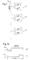
- Fig. 1 shows a diagram of a generic communication channel 1 on which devices D1, D2, ... Dn are connected.
- the communication channel can, for example, be a communication bus, on which there can be present a voltage that is subjected to a series of transitions between a high value (“Vbus") and a low value (“gnd") to generate information bits that are transmitted over the communication bus.
- Voltage modulation on the bus is determined by the transmission of data by the devices D1, D2, ... Dn according to a protocol, whose structure is not important in order to understand the present invention and can be any. The only thing that is important is that a data stream containing a plurality of transitions between the voltage values (in the example illustrated two values "Vbus", "gnd”) is present on the communication bus 1.
- Fig. 1A shows two symbols, defined as "1" and "0", which can be used to communicate information on the communication channel 1.
- Each symbol is formed by a sequence of a given number of bits.
- Each bit has a duration T com , while each symbol has a duration equal to a multiple of the duration of one bit.
- the duration T symbol of a symbol is 4T com , as each symbol is formed of four bits.
- the symbol defined as "1” is constituted by a first bit during which the voltage on the communication channel is equal to the low value “gnd” and three bits during which the voltage is at the high value "Vbus".
- the symbol “0” is encoded as sequence of four bits, the first three of which are at the low value "gnd” and the last at the high value "Vbus”. It must be understood that various other symbols can also be provided, defined by other sequences of bits and that other transmission protocols can also be provided, in which each symbol is constituted by a sequence of bits of a length other than the one shown.
- the single devices D1, D2, ... Dn must phase their internal clock to the data stream on the communication channel 1 to be able to dialog correctly on the communication channel 1.
- the clock frequency must be set as a function of the transmission frequency and the phase of the clock signal must allow the device to "lock" the phase of the data stream transmitted on the transmission channel to allow both data recovery, i.e. correct sampling and consequently correct interpretation of the data, and correct transmission of information from the device to the communication channel.
- the internal clock of a generic device D1 has a frequency substantially equal to the communication frequency or to a multiple of said frequency.
- a clock frequency equal to the value of the communication frequency is advantageously provided.
- This clock frequency is the lowest admissible for an operation of locking and recovery of the signal on the communication channel, to the advantage of limiting computational complexity.
- the phase of the clock signal must be locked to the phase of the data stream on the channel 1, i.e. each device D1, D2, ... Dn that must communicate through the channel 1 must have its own clock synchronized with the data stream on the channel.
- Synchronized is intended in general as a signal that has a desired phase shift with respect to the data stream, not necessarily a phase shift equal to zero.
- the device is provided with a phase detector circuit, shown schematically in Fig. 2 and indicated as a whole with 3, which supplies in the manner described below an input signal for a PLL.
- the phase detector circuit 3 comprises a sample-and-hold circuit 5 with an input 5A for the signal to be sampled.
- An input B of a phase comparator 7 is connected to the output of the sample-and-hold circuit 5.
- the phase comparator 7 comprise a further input A and an output Y.
- the data stream coming from the communication channel, indicated in Fig. 2 as "bus signal”, is applied to the input A of the phase comparator 7 and to the input 5A of the sample-and-hold circuit 5.
- the sample-and-hold circuit 5 is controlled by the clock signal CLK of the device, for example generated by a digital phase-controlled oscillator.
- the clock signal CLK has a frequency typically equal to the communication frequency on the communication channel 1. Therefore, a digital signal representing the recovery of the signal present on the communication bus 1 is present on the output of the sample-and-hold circuit 5.
- the phase shift between the bus signal and the recovered signal depends on the phase of the clock signal.
- the block 5, which represents the sample-and-hold circuit comprises in a manner known per se an electronic switch 11 (for example a MOSFET), whose closing and opening is controlled by the clock signal CLK. Closing of the electronic switch 11 places the input 5A of the sample-and-hold circuit in communication with a capacitor 13 and the noninverting input of an operational amplifier 15 whose inverting input is connected to the output of the amplifier.
- the amplifier 15 functions as an output buffer.
- the phase comparator is formed by an exclusive OR (X-OR) logic gate.
- X-OR exclusive OR
- the truth table of this logic gate is, as it is known, the following: A B Y L L L L H H H L H H H L L and H being two generic digitalized levels that the signals on the inputs A and B of the gate can take.
- the output of the gate is "H" only if the input signals are different from each other.
- L and H indicate the two levels that the signal on the communication bus 1 can take, for example L can be the low value ("gnd") and H the high value ("Vbus”) of the bus voltage.
- Fig. 3 shows the shape of the signal on the inputs A and B and on the output Y of the phase comparator 7, A being the signal coming from the communication bus 1, B the sampled signal, i.e. the signal recovered from the sample-and-hold circuit 5, Y the output signal of the phase comparator 7 and CLK the clock signal on the basis of which sampling is performed. Sampling takes place at each raising edge of the CLK signal.
- the output Y of the X-OR gate is low (L) and is maintained at this value until the subsequent raising edge of the signal on the bus (input A), at the instant t 1 .
- the output signal Y of the X-OR gate 7 goes to the high value (H) as the two inputs A and B are different from each other. This high value of the output Y is maintained until the subsequent sampling instant t 2 , which coincides with the raising edge of the clock signal CLK.
- the output signal Y returns to low, as the signal on the first input A (bus signal) and the signal on the second input B (sampled signal) have the same high value, resulting from the sample-and-hold operation.
- the subsequent raising edge of the output signal Y is obtained at the instant t 3 , when the bus signal on the input A goes to the low value, while the signal on the input B is maintained high by the sample-and-hold signal 5.
- the subsequent sampling instant is obtained at the instant t 4 , at the subsequent raising edge of the clock signal CLK, coinciding with which the signal Y has a falling edge, and so forth.
- the duration of the high part ("H") of the output signal Y corresponds to the delay, i.e. the phase shift between the signals A and B.
- the phase shift between the two signals equal to T_delay ( Fig. 3 ) is given by the time interval during which the output signal Y of the X-OR gate takes a high value (H).
- the output signal Y of the phase detector circuit is such that the duration of the high pulse (H) is equal to the phase shift between the bus signal (and therefore the data stream on the bus 1) and the digital signal recovered by the sample-and-hold circuit 5.
- the phase detector circuit 3 forms part of a PLL circuit, in which the output signal of the phase comparator 7 is used as phase error signal.
- the PLL circuit hereinafter described with reference to Figs 5 and 6 , is designed to make the phase error signal converge toward a desired phase shift value between the data stream and the signal sampled by the sample-and-hold circuit 5. This is obtained by acting on the phase of the clock signal generated by the oscillator of the PLL circuit.
- the phase detector circuit 3 has an important property that can be expressed as follows: a falling transition edge (i.e. from the high value to the low value) of the output signal Y of the phase detector signal 3 always coincides with a raising transition edge of the clock signal CLK.
- This property is important for the purposes of calculating the duration of the high pulse of the output signal Y. In fact, it allows the use of a time calculation mode called Gated Count Mode.
- the delay time i.e. the phase shift between the bus signal A and the sampled signal B, this delay being defined by the time interval during which the signal Y remains high.
- This duration is calculated through a block 20 defined as time interval extractor block, indicated as ⁇ T-extractor in the block diagram of Fig. 5 .
- it is a digital timer, whose function is that of extracting a time value from the input signal.
- a free running timer which is sampled by the control algorithm at a fixed frequency, can be used for this purpose. It can use, for example, a count mode called "Gated Count Mode" or a count mode called "Input Capture Mode". The first mode is preferred.
- the timer is started when the input signal makes a raising transition and the count is sampled at the falling transition of the signal Y.
- the timer can be controlled by software through the clock signal CLK. The aforesaid property allows resetting of the time measured at each raising edge of the clock signal also in the absence of synchronism.
- the Input Capture Mode counts the time between two edges of an input signal. This count mode can also be used, as it is the time between two consecutive edges (raising and falling respectively) of the output signal Y of the phase detector circuit 3 that must be measured.
- the output of the block 20, indicated with T_Delay in the block diagram of Fig. 5 is a digital measurement of the time duration of the interval during which the signal Y is at the high value, time that corresponds to the phase shift between the bus signal and the sampled signal.
- This time value is sent to a delay shifter block 30, called "time interval shifter” or ⁇ T-Shifter.
- the function of this block is as follows: if the value T_Delay calculated by the block 20 is comprised between 0 and T CLK /2 (where T CLK is the clock time) the delay T_Delay calculated by the block 20 remains unchanged. If the delay T_Delay is comprised between T CLK /2 and T CLK , its value is translated by T CLK .
- T_Delay Mod ⁇ T_Delay if 0 ⁇ T_Delay ⁇ T CLK 2 T_Delay - T CLK if T CLK 2 ⁇ T_Delay ⁇ T CLK
- the signal T_Delay Mod is filtered in a filter block LP (Loop Filter) indicated with 40, which will be described below, and the output signal from the filter, indicated with T_Delay Mod Avg is supplied to a proportional integral compensator PI, indicated with 50.
- This block is constituted by a digital proportional-integral compensator in the domain Z and supplies a DPCO (Digital Phase-Controlled Oscillator) 60 with a signal that represents a phase variation ( ⁇ phase) to obtain phase locking of the clock signal to the data stream on the communication channel 1.
- DPCO Digital Phase-Controlled Oscillator
- the proportional integral compensator 50 can have the structure represented by the block diagram of Fig. 6 .
- the PI compensator receives the input signal T_Delay Mod Avg and a desired phase shift value between the clock signal and the data stream. This desired phase shift is indicated as "Target Delay" and is supplied by a block 52.
- this desired delay can be 0 (i.e. the sampled signal is in phase with the data stream on the communication channel).
- the delay can typically be comprised between 0 and T CLK /2, for example can be equal to T CLK /3.
- Target_Delay[n] The difference between the Target_Delay value at the step n of the algorithm (Target_Delay[n]) and the value T_Delay Mod Avg at the step n (T_Delay Mod Avg [n]) is multiplied by a gain constant ⁇ and added to the value of the phase variation calculated at the preceding step (n-1) to obtain the value of the phase variation ( ⁇ phase[n-1]) at the current step [n] of the control algorithm. This value ( ⁇ phase[n]) is supplied to the control input of the oscillator 60.
- the value of the gain constant ⁇ is chosen on the basis of some considerations on the closed loop transfer function of the PLL.
- h LPF [n] represents the response of the filter 40 to the pulse and will be described subsequently and the symbol ⁇ indicates the convolution operation.
- the block 60 is a square wave generator that has two inputs and one output., The first input supplies the square wave frequency that must be generated, while the second input is a phase input and comes from the block 50.
- the output of the block 60 is the clock signal CLK that controls the sample-and-hold circuit 3.
- the frequency of the clock signal CLK is advantageously set equal to the value of the transmission frequency.
- a sampling delay is also applied, through the block 70, to the clock signal generated by the digital voltage controlled oscillator 60.
- T BUS max T RISE T FALL This time T BUS is added to the sampling signal generated by the PLL circuit, so that sampling is always carried out after the signal has completed the raising or falling edge.
- Figs 7 to 9 show the waveforms of the communication signal on the bus, of the recovered signal, of the clock signal and of the delay between the bus signal and the recovered signal in three different operating conditions.
- A indicates the bus signal, i.e. the data stream on the communication bus 1
- B indicates the signal recovered through the PLL circuit described above
- CLK indicates the clock signal
- ⁇ T indicates the delay between the signals A and B.
- the delay ⁇ T is equal to the desired delay (Target_Delay) set by the block 52.
- Fig. 8 shows the waveforms in the case of a set delay between the signals A and B equal to T CLK /4, i.e. to a quarter of the clock period, while Fig. 9 shows the same waveforms with a set delay equal to T CLK /3.
Landscapes
- Engineering & Computer Science (AREA)
- Computer Networks & Wireless Communication (AREA)
- Signal Processing (AREA)
- Synchronisation In Digital Transmission Systems (AREA)
- Stabilization Of Oscillater, Synchronisation, Frequency Synthesizers (AREA)
Claims (18)
- Un procédé de reconstitution d'horloge et reconstitution de données à partir d'un flux de données sur un canal de communication (1), comprenant les étapes consistant à :- échantillonner un flux de données sur ledit canal de communication (1) et à une fréquence d'échantillonnage déterminée par un signal d'horloge (CLK) et générer un signal échantillonné ;- déterminer un décalage de phase entre un flux de données de communication et le signal échantillonné en appliquant le signal échantillonné et le flux de données à deux entrées d'un comparateur de phases (7) qui fournit un signal de décalage de phase de sortie (Y), caractérisé par les étapes consistant à :- appliquer ledit signal de décalage de phase à un bloc de calcul d'un temps de retard (20) entre deux bords du signal de décalage de phase, pour fournir un signal qui est fonction dudit temps de retard ;- appliquer un signal qui est fonction du délai de retard à un compensateur (50), dont la sortie modifie la phase dudit signal d'horloge (CLK) sur la base dudit décalage de phase, afin d'obtenir une différence de phase souhaitée entre ledit signal échantillonné et ledit flux de données.
- Procédé selon la revendication 1, dans lequel ledit flux de données est échantillonné à un point prédéterminé du signal d'horloge.
- Procédé selon la revendication 1 ou 2, dans lequel ledit flux de données est échantillonné à travers un circuit échantillonneur-bloqueur (5).
- Procédé selon une ou plusieurs des revendications précédentes, dans lequel ledit flux de données est échantillonné aux bords croissants dudit signal d'horloge (CLK).
- Procédé selon une ou plusieurs des revendications précédentes, comprenant l'étape d'estimation d'une fréquence de transmission du flux de données et dans lequel la fréquence du signal d'horloge (CLK) est fixée en fonction de la fréquence de transmission du flux de données.
- Procédé selon une ou plusieurs des revendications précédentes, dans lequel ledit signal de décalage de phase (Y) est généré en appliquant le flux de données et le signal échantillonné aux entrées (A,B) d'une porte logique OU exclusif (7), et dans lequel le signal de décalage de phase (Y) est déterminé par le signal de sortie de ladite porte logique (7).
- Procédé selon une ou plusieurs des revendications précédentes, dans lequel ledit signal d'horloge (CLK) est modifié en fonction dudit signal de décalage de phase.
- Procédé selon une ou plusieurs des revendications précédentes, dans lequel ledit compensateur (50) est un compensateur proportionnel-intégral.
- Procédé selon une ou plusieurs des revendications précédentes, dans lequel la sortie dudit compensateur (50) est appliquée à un général de signal d'horloge (60).
- Procédé selon la revendication 9, dans lequel un signal indiquant ladite différence souhaitée de phase entre le signal échantillonné et le flux de données est appliqué audit générateur de signal d'horloge (60).
- Procédé selon la revendication 9 ou 10, dans lequel la sortie dudit générateur de signal d'horloge (60) est appliquée à un bloc de retard d'échantillonnage (70) et la sortie du bloc de retard (70) est utilisée pour commander l'échantillonnage du flux de données.
- Un circuit de reconstitution d'horloge et de reconstitution de données à partir d'un flux de données sur un canal de communication, comprenant un circuit PLL (boucle de verrouillage de phase) comprenant :- un oscillateur qui génère un signal d'horloge à une fréquence d'horloge ;- un circuit de détection de phase comprenant :a. une entrée (5A) pour ledit flux de données à une fréquence de communication ;b. un circuit échantillonneur-bloqueur (5) commandé par un signal d'échantillonnage à une fréquence d' échantillonnage ;c. un comparateur de phases (7) avec une première entrée (A) à laquelle le flux de données est appliqué et une seconde entrée (B) à laquelle un signal échantillonné par ledit circuit échantillonneur-bloqueur (5) est appliqué, la sortie (Y) dudit comparateur de phase (7) étant un signal de phase qui est fonction de la différence de phase entre ledit flux de données et ledit signal échantillonné ;- un bloc extracteur d'intervalle de temps (20) pour déterminer la durée dudit signal de phase (Y), à une entrée duquel ledit signal de phase est appliqué ;- un compensateur (50) dont l'entrée reçoit un signal qui est fonction du signal de phase et dont la sortie fournit un signal de variation de phase agissant comme signal de commande pour ledit oscillateur (60), lequel modifie la phase du signal d'horloge dudit oscillateur de manière à faire converger la différence de phase entre le signal échantillonné et le flux de données vers une différence de phase souhaitée.
- Circuit selon la revendication 12, dans lequel ladite fréquence d'échantillonnage est fonction d'une fréquence de communication.
- Circuit selon la revendication 12 ou 13, dans lequel un bloc de décalage d'intervalle de temps (30) est associé avec ledit block extracteur d'intervalle de temps (20).
- Circuit selon une ou plusieurs des revendications 12 à 14, dans lequel ladite fréquence d'échantillonnage est fonction de la fréquence de communication.
- Circuit selon une ou plusieurs des revendications 12 à 15, dans lequel ledit comparateur de phase comprend une porte logique OU exclusif (7).
- Circuit selon une ou plusieurs des revendications 12 à 16, dans lequel ledit compensateur (50) est un compensateur proportionnel-intégral.
- Circuit selon la revendication 17, comprenant un bloc de retard d'échantillonnage (70) qui impose un retard au signal d'échantillonnage en fonction du temps de transition de niveau maximal du flux de données.
Applications Claiming Priority (1)
| Application Number | Priority Date | Filing Date | Title |
|---|---|---|---|
| PCT/IT2010/000468 WO2012070073A1 (fr) | 2010-11-23 | 2010-11-23 | Procédé et circuit de reconstitution d'horloge à partir d'une description de flux de données |
Publications (2)
| Publication Number | Publication Date |
|---|---|
| EP2643929A1 EP2643929A1 (fr) | 2013-10-02 |
| EP2643929B1 true EP2643929B1 (fr) | 2015-08-12 |
Family
ID=44477679
Family Applications (1)
| Application Number | Title | Priority Date | Filing Date |
|---|---|---|---|
| EP10807749.6A Not-in-force EP2643929B1 (fr) | 2010-11-23 | 2010-11-23 | Procédé et circuit de reconstitution d'horloge à partir d'un flux de données |
Country Status (4)
| Country | Link |
|---|---|
| US (1) | US9031182B2 (fr) |
| EP (1) | EP2643929B1 (fr) |
| ES (1) | ES2551583T3 (fr) |
| WO (1) | WO2012070073A1 (fr) |
Families Citing this family (9)
| Publication number | Priority date | Publication date | Assignee | Title |
|---|---|---|---|---|
| US11507310B2 (en) * | 2019-09-02 | 2022-11-22 | SK Hynix Inc. | Memory controller and operating method thereof |
| KR20210061174A (ko) | 2019-11-19 | 2021-05-27 | 에스케이하이닉스 주식회사 | 메모리 컨트롤러 및 그 동작 방법 |
| US11501808B2 (en) | 2019-09-02 | 2022-11-15 | SK Hynix Inc. | Memory controller and operating method thereof |
| KR102713219B1 (ko) | 2019-09-02 | 2024-10-07 | 에스케이하이닉스 주식회사 | 메모리 컨트롤러 및 그 동작 방법 |
| KR20210097938A (ko) | 2020-01-31 | 2021-08-10 | 에스케이하이닉스 주식회사 | 클록변조를 통해 리드 데이터의 신뢰성을 검증하는 메모리 장치 및 메모리 장치를 포함하는 메모리 시스템 |
| US12051470B2 (en) | 2019-09-02 | 2024-07-30 | SK Hynix Inc. | Memory controller and operating method thereof |
| US11184008B2 (en) * | 2019-11-08 | 2021-11-23 | Nvidia Corp. | Data recovery technique for time interleaved receiver in presence of transmitter pulse width distortion |
| CN116318516B (zh) * | 2023-05-25 | 2023-08-15 | 芯动微电子科技(珠海)有限公司 | 基于dp协议的再生流时钟动态精准实现方法及设备 |
| CN116743158B (zh) * | 2023-08-15 | 2023-11-07 | 慷智集成电路(上海)有限公司 | 提取输入信号频率相位的方法及数字信号传输系统 |
Family Cites Families (10)
| Publication number | Priority date | Publication date | Assignee | Title |
|---|---|---|---|---|
| GB2138227B (en) * | 1983-04-12 | 1987-02-04 | Sony Corp | Digital video tape recorder apparatus |
| US5850422A (en) * | 1995-07-21 | 1998-12-15 | Symbios, Inc. | Apparatus and method for recovering a clock signal which is embedded in an incoming data stream |
| DE60231266D1 (de) * | 2001-03-07 | 2009-04-09 | Nippon Telegraph & Telephone | Schaltung zur Daten-und Taktrückgewinnung |
| US6930628B2 (en) * | 2001-05-03 | 2005-08-16 | Coreoptics, Inc. | Amplitude detection for controlling the decision instant for sampling as a data flow |
| GB2397956B (en) | 2003-01-29 | 2005-11-30 | Phyworks Ltd | Phase detector |
| US20040218705A1 (en) * | 2003-01-30 | 2004-11-04 | International Business Machines Corporation | Phase rotator, phase rotation method and clock and data recovery receiver incorporating said phase rotator |
| US20050058235A1 (en) * | 2003-09-17 | 2005-03-17 | Beeson David A. | Clock and data recovery system for a wide range of bit rates |
| KR100711095B1 (ko) * | 2005-08-11 | 2007-04-24 | 삼성전자주식회사 | 클럭 및 데이터 복원회로, 및 클럭 및 데이터 복원 방법 |
| US7764759B2 (en) * | 2006-06-13 | 2010-07-27 | Gennum Corporation | Linear sample and hold phase detector for clocking circuits |
| US8249207B1 (en) * | 2008-02-29 | 2012-08-21 | Pmc-Sierra, Inc. | Clock and data recovery sampler calibration |
-
2010
- 2010-11-23 WO PCT/IT2010/000468 patent/WO2012070073A1/fr not_active Ceased
- 2010-11-23 ES ES10807749.6T patent/ES2551583T3/es active Active
- 2010-11-23 EP EP10807749.6A patent/EP2643929B1/fr not_active Not-in-force
-
2013
- 2013-05-20 US US13/897,731 patent/US9031182B2/en not_active Expired - Fee Related
Also Published As
| Publication number | Publication date |
|---|---|
| US9031182B2 (en) | 2015-05-12 |
| ES2551583T3 (es) | 2015-11-20 |
| EP2643929A1 (fr) | 2013-10-02 |
| US20140023169A1 (en) | 2014-01-23 |
| WO2012070073A1 (fr) | 2012-05-31 |
Similar Documents
| Publication | Publication Date | Title |
|---|---|---|
| US9031182B2 (en) | Method and circuit for clock recovery of a data stream description | |
| CN102752097B (zh) | 符号时钟恢复电路 | |
| JPH01161936A (ja) | デジタルpllによるクロック回復装置 | |
| US20100241918A1 (en) | Clock and data recovery for differential quadrature phase shift keying | |
| JP2010056989A (ja) | 信号再生回路向け位相比較回路及び信号再生回路向け位相比較回路を備える光通信装置 | |
| KR101733660B1 (ko) | 10gbase―t 시스템에서 데이터 보조 타이밍 복원을 위한 방법 및 장치 | |
| CN107222219A (zh) | 具备帧对齐功能的高速串并转换电路 | |
| US10116433B2 (en) | Circuit arrangement and method for clock and data recovery | |
| JP2010183452A (ja) | クロック生成回路 | |
| WO2008044407A1 (fr) | Dispositif de récupération de données d'horloge | |
| CN119356481B (zh) | 一种波形同步方法、装置和同步波形产生设备 | |
| EP2985610A1 (fr) | Procédé pour déterminer une forme d'onde corrélée sur un oscilloscope en temps réel | |
| US8824615B2 (en) | Frequency tracing circuit and method thereof | |
| JP4340390B2 (ja) | ディジタル形式の信号のサンプリング中にクロック再生する方法 | |
| EP3160077A1 (fr) | Appareil de récupération d'horloge et procédé de récupération d'horloge | |
| US6791420B2 (en) | Phase locked loop for recovering a clock signal from a data signal | |
| TWI332763B (en) | Usb device, frequency auto-locking device and frequency auto-locking method | |
| US6680991B1 (en) | Detection of frequency differences between signals | |
| CN103378823B (zh) | 运用脉波辨识的频率产生方法与系统 | |
| CN117349093B (zh) | 眼图监测电路、芯片及电子设备 | |
| CN115176509A (zh) | 根据tdma协议在主设备与至少一个从设备之间进行通信的方法 | |
| JP3994545B2 (ja) | データ受信装置 | |
| CN114696597B (zh) | 一种充电泵电路、鉴频鉴相器和改进型锁相环电路 | |
| US8774325B2 (en) | Clock and data recovery circuits | |
| JP2000124801A (ja) | Pll回路 |
Legal Events
| Date | Code | Title | Description |
|---|---|---|---|
| PUAI | Public reference made under article 153(3) epc to a published international application that has entered the european phase |
Free format text: ORIGINAL CODE: 0009012 |
|
| 17P | Request for examination filed |
Effective date: 20130605 |
|
| AK | Designated contracting states |
Kind code of ref document: A1 Designated state(s): AL AT BE BG CH CY CZ DE DK EE ES FI FR GB GR HR HU IE IS IT LI LT LU LV MC MK MT NL NO PL PT RO RS SE SI SK SM TR |
|
| DAX | Request for extension of the european patent (deleted) | ||
| RAP1 | Party data changed (applicant data changed or rights of an application transferred) |
Owner name: ABB TECHNOLOGY AG |
|
| GRAP | Despatch of communication of intention to grant a patent |
Free format text: ORIGINAL CODE: EPIDOSNIGR1 |
|
| INTG | Intention to grant announced |
Effective date: 20150303 |
|
| GRAS | Grant fee paid |
Free format text: ORIGINAL CODE: EPIDOSNIGR3 |
|
| GRAA | (expected) grant |
Free format text: ORIGINAL CODE: 0009210 |
|
| AK | Designated contracting states |
Kind code of ref document: B1 Designated state(s): AL AT BE BG CH CY CZ DE DK EE ES FI FR GB GR HR HU IE IS IT LI LT LU LV MC MK MT NL NO PL PT RO RS SE SI SK SM TR |
|
| REG | Reference to a national code |
Ref country code: GB Ref legal event code: FG4D |
|
| REG | Reference to a national code |
Ref country code: CH Ref legal event code: EP |
|
| REG | Reference to a national code |
Ref country code: AT Ref legal event code: REF Ref document number: 742923 Country of ref document: AT Kind code of ref document: T Effective date: 20150815 |
|
| REG | Reference to a national code |
Ref country code: IE Ref legal event code: FG4D |
|
| REG | Reference to a national code |
Ref country code: DE Ref legal event code: R096 Ref document number: 602010026689 Country of ref document: DE |
|
| REG | Reference to a national code |
Ref country code: ES Ref legal event code: FG2A Ref document number: 2551583 Country of ref document: ES Kind code of ref document: T3 Effective date: 20151120 |
|
| REG | Reference to a national code |
Ref country code: FR Ref legal event code: PLFP Year of fee payment: 6 |
|
| REG | Reference to a national code |
Ref country code: LT Ref legal event code: MG4D |
|
| REG | Reference to a national code |
Ref country code: AT Ref legal event code: MK05 Ref document number: 742923 Country of ref document: AT Kind code of ref document: T Effective date: 20150812 |
|
| REG | Reference to a national code |
Ref country code: NL Ref legal event code: MP Effective date: 20150812 |
|
| PG25 | Lapsed in a contracting state [announced via postgrant information from national office to epo] |
Ref country code: GR Free format text: LAPSE BECAUSE OF FAILURE TO SUBMIT A TRANSLATION OF THE DESCRIPTION OR TO PAY THE FEE WITHIN THE PRESCRIBED TIME-LIMIT Effective date: 20151113 Ref country code: NO Free format text: LAPSE BECAUSE OF FAILURE TO SUBMIT A TRANSLATION OF THE DESCRIPTION OR TO PAY THE FEE WITHIN THE PRESCRIBED TIME-LIMIT Effective date: 20151112 Ref country code: LT Free format text: LAPSE BECAUSE OF FAILURE TO SUBMIT A TRANSLATION OF THE DESCRIPTION OR TO PAY THE FEE WITHIN THE PRESCRIBED TIME-LIMIT Effective date: 20150812 Ref country code: LV Free format text: LAPSE BECAUSE OF FAILURE TO SUBMIT A TRANSLATION OF THE DESCRIPTION OR TO PAY THE FEE WITHIN THE PRESCRIBED TIME-LIMIT Effective date: 20150812 Ref country code: FI Free format text: LAPSE BECAUSE OF FAILURE TO SUBMIT A TRANSLATION OF THE DESCRIPTION OR TO PAY THE FEE WITHIN THE PRESCRIBED TIME-LIMIT Effective date: 20150812 |
|
| PG25 | Lapsed in a contracting state [announced via postgrant information from national office to epo] |
Ref country code: SE Free format text: LAPSE BECAUSE OF FAILURE TO SUBMIT A TRANSLATION OF THE DESCRIPTION OR TO PAY THE FEE WITHIN THE PRESCRIBED TIME-LIMIT Effective date: 20150812 Ref country code: RS Free format text: LAPSE BECAUSE OF FAILURE TO SUBMIT A TRANSLATION OF THE DESCRIPTION OR TO PAY THE FEE WITHIN THE PRESCRIBED TIME-LIMIT Effective date: 20150812 Ref country code: PT Free format text: LAPSE BECAUSE OF FAILURE TO SUBMIT A TRANSLATION OF THE DESCRIPTION OR TO PAY THE FEE WITHIN THE PRESCRIBED TIME-LIMIT Effective date: 20151214 Ref country code: PL Free format text: LAPSE BECAUSE OF FAILURE TO SUBMIT A TRANSLATION OF THE DESCRIPTION OR TO PAY THE FEE WITHIN THE PRESCRIBED TIME-LIMIT Effective date: 20150812 Ref country code: HR Free format text: LAPSE BECAUSE OF FAILURE TO SUBMIT A TRANSLATION OF THE DESCRIPTION OR TO PAY THE FEE WITHIN THE PRESCRIBED TIME-LIMIT Effective date: 20150812 Ref country code: IS Free format text: LAPSE BECAUSE OF FAILURE TO SUBMIT A TRANSLATION OF THE DESCRIPTION OR TO PAY THE FEE WITHIN THE PRESCRIBED TIME-LIMIT Effective date: 20151212 Ref country code: AT Free format text: LAPSE BECAUSE OF FAILURE TO SUBMIT A TRANSLATION OF THE DESCRIPTION OR TO PAY THE FEE WITHIN THE PRESCRIBED TIME-LIMIT Effective date: 20150812 |
|
| PG25 | Lapsed in a contracting state [announced via postgrant information from national office to epo] |
Ref country code: NL Free format text: LAPSE BECAUSE OF FAILURE TO SUBMIT A TRANSLATION OF THE DESCRIPTION OR TO PAY THE FEE WITHIN THE PRESCRIBED TIME-LIMIT Effective date: 20150812 |
|
| PG25 | Lapsed in a contracting state [announced via postgrant information from national office to epo] |
Ref country code: EE Free format text: LAPSE BECAUSE OF FAILURE TO SUBMIT A TRANSLATION OF THE DESCRIPTION OR TO PAY THE FEE WITHIN THE PRESCRIBED TIME-LIMIT Effective date: 20150812 Ref country code: DK Free format text: LAPSE BECAUSE OF FAILURE TO SUBMIT A TRANSLATION OF THE DESCRIPTION OR TO PAY THE FEE WITHIN THE PRESCRIBED TIME-LIMIT Effective date: 20150812 Ref country code: SK Free format text: LAPSE BECAUSE OF FAILURE TO SUBMIT A TRANSLATION OF THE DESCRIPTION OR TO PAY THE FEE WITHIN THE PRESCRIBED TIME-LIMIT Effective date: 20150812 Ref country code: CZ Free format text: LAPSE BECAUSE OF FAILURE TO SUBMIT A TRANSLATION OF THE DESCRIPTION OR TO PAY THE FEE WITHIN THE PRESCRIBED TIME-LIMIT Effective date: 20150812 |
|
| REG | Reference to a national code |
Ref country code: DE Ref legal event code: R097 Ref document number: 602010026689 Country of ref document: DE |
|
| PG25 | Lapsed in a contracting state [announced via postgrant information from national office to epo] |
Ref country code: RO Free format text: LAPSE BECAUSE OF FAILURE TO SUBMIT A TRANSLATION OF THE DESCRIPTION OR TO PAY THE FEE WITHIN THE PRESCRIBED TIME-LIMIT Effective date: 20150812 |
|
| REG | Reference to a national code |
Ref country code: CH Ref legal event code: NV Representative=s name: ISLER AND PEDRAZZINI AG, CH |
|
| PLBE | No opposition filed within time limit |
Free format text: ORIGINAL CODE: 0009261 |
|
| STAA | Information on the status of an ep patent application or granted ep patent |
Free format text: STATUS: NO OPPOSITION FILED WITHIN TIME LIMIT |
|
| PG25 | Lapsed in a contracting state [announced via postgrant information from national office to epo] |
Ref country code: LU Free format text: LAPSE BECAUSE OF FAILURE TO SUBMIT A TRANSLATION OF THE DESCRIPTION OR TO PAY THE FEE WITHIN THE PRESCRIBED TIME-LIMIT Effective date: 20151123 Ref country code: MC Free format text: LAPSE BECAUSE OF FAILURE TO SUBMIT A TRANSLATION OF THE DESCRIPTION OR TO PAY THE FEE WITHIN THE PRESCRIBED TIME-LIMIT Effective date: 20150812 |
|
| 26N | No opposition filed |
Effective date: 20160513 |
|
| REG | Reference to a national code |
Ref country code: IE Ref legal event code: MM4A |
|
| PG25 | Lapsed in a contracting state [announced via postgrant information from national office to epo] |
Ref country code: SI Free format text: LAPSE BECAUSE OF FAILURE TO SUBMIT A TRANSLATION OF THE DESCRIPTION OR TO PAY THE FEE WITHIN THE PRESCRIBED TIME-LIMIT Effective date: 20150812 |
|
| PG25 | Lapsed in a contracting state [announced via postgrant information from national office to epo] |
Ref country code: IE Free format text: LAPSE BECAUSE OF NON-PAYMENT OF DUE FEES Effective date: 20151123 |
|
| REG | Reference to a national code |
Ref country code: FR Ref legal event code: PLFP Year of fee payment: 7 |
|
| PG25 | Lapsed in a contracting state [announced via postgrant information from national office to epo] |
Ref country code: BE Free format text: LAPSE BECAUSE OF FAILURE TO SUBMIT A TRANSLATION OF THE DESCRIPTION OR TO PAY THE FEE WITHIN THE PRESCRIBED TIME-LIMIT Effective date: 20150812 |
|
| REG | Reference to a national code |
Ref country code: DE Ref legal event code: R082 Ref document number: 602010026689 Country of ref document: DE Representative=s name: GLAWE DELFS MOLL PARTNERSCHAFT MBB VON PATENT-, DE Ref country code: DE Ref legal event code: R081 Ref document number: 602010026689 Country of ref document: DE Owner name: ABB SCHWEIZ AG, CH Free format text: FORMER OWNER: ABB TECHNOLOGY AG, ZUERICH, CH Ref country code: DE Ref legal event code: R081 Ref document number: 602010026689 Country of ref document: DE Owner name: MARICI HOLDINGS THE NETHERLANDS B.V., NL Free format text: FORMER OWNER: ABB TECHNOLOGY AG, ZUERICH, CH |
|
| PG25 | Lapsed in a contracting state [announced via postgrant information from national office to epo] |
Ref country code: SM Free format text: LAPSE BECAUSE OF FAILURE TO SUBMIT A TRANSLATION OF THE DESCRIPTION OR TO PAY THE FEE WITHIN THE PRESCRIBED TIME-LIMIT Effective date: 20150812 Ref country code: HU Free format text: LAPSE BECAUSE OF FAILURE TO SUBMIT A TRANSLATION OF THE DESCRIPTION OR TO PAY THE FEE WITHIN THE PRESCRIBED TIME-LIMIT; INVALID AB INITIO Effective date: 20101123 Ref country code: BG Free format text: LAPSE BECAUSE OF FAILURE TO SUBMIT A TRANSLATION OF THE DESCRIPTION OR TO PAY THE FEE WITHIN THE PRESCRIBED TIME-LIMIT Effective date: 20150812 |
|
| PG25 | Lapsed in a contracting state [announced via postgrant information from national office to epo] |
Ref country code: CY Free format text: LAPSE BECAUSE OF FAILURE TO SUBMIT A TRANSLATION OF THE DESCRIPTION OR TO PAY THE FEE WITHIN THE PRESCRIBED TIME-LIMIT Effective date: 20150812 |
|
| PG25 | Lapsed in a contracting state [announced via postgrant information from national office to epo] |
Ref country code: MT Free format text: LAPSE BECAUSE OF FAILURE TO SUBMIT A TRANSLATION OF THE DESCRIPTION OR TO PAY THE FEE WITHIN THE PRESCRIBED TIME-LIMIT Effective date: 20150812 |
|
| REG | Reference to a national code |
Ref country code: FR Ref legal event code: PLFP Year of fee payment: 8 |
|
| REG | Reference to a national code |
Ref country code: ES Ref legal event code: PC2A Owner name: ABB SCHWEIZ AG Effective date: 20171213 |
|
| REG | Reference to a national code |
Ref country code: CH Ref legal event code: PFUS Owner name: ABB SCHWEIZ AG, CH Free format text: FORMER OWNER: ABB TECHNOLOGY AG, CH |
|
| REG | Reference to a national code |
Ref country code: GB Ref legal event code: 732E Free format text: REGISTERED BETWEEN 20180426 AND 20180502 |
|
| PG25 | Lapsed in a contracting state [announced via postgrant information from national office to epo] |
Ref country code: MK Free format text: LAPSE BECAUSE OF FAILURE TO SUBMIT A TRANSLATION OF THE DESCRIPTION OR TO PAY THE FEE WITHIN THE PRESCRIBED TIME-LIMIT Effective date: 20150812 Ref country code: TR Free format text: LAPSE BECAUSE OF FAILURE TO SUBMIT A TRANSLATION OF THE DESCRIPTION OR TO PAY THE FEE WITHIN THE PRESCRIBED TIME-LIMIT Effective date: 20150812 |
|
| REG | Reference to a national code |
Ref country code: FR Ref legal event code: TP Owner name: ABB SCHWEIZ AG, CH Effective date: 20180912 |
|
| PG25 | Lapsed in a contracting state [announced via postgrant information from national office to epo] |
Ref country code: AL Free format text: LAPSE BECAUSE OF FAILURE TO SUBMIT A TRANSLATION OF THE DESCRIPTION OR TO PAY THE FEE WITHIN THE PRESCRIBED TIME-LIMIT Effective date: 20150812 |
|
| PGFP | Annual fee paid to national office [announced via postgrant information from national office to epo] |
Ref country code: FR Payment date: 20191120 Year of fee payment: 10 |
|
| PGFP | Annual fee paid to national office [announced via postgrant information from national office to epo] |
Ref country code: CH Payment date: 20191121 Year of fee payment: 10 |
|
| PGFP | Annual fee paid to national office [announced via postgrant information from national office to epo] |
Ref country code: GB Payment date: 20191120 Year of fee payment: 10 |
|
| REG | Reference to a national code |
Ref country code: DE Ref legal event code: R082 Ref document number: 602010026689 Country of ref document: DE Representative=s name: GLAWE DELFS MOLL PARTNERSCHAFT MBB VON PATENT-, DE Ref country code: DE Ref legal event code: R081 Ref document number: 602010026689 Country of ref document: DE Owner name: MARICI HOLDINGS THE NETHERLANDS B.V., NL Free format text: FORMER OWNER: ABB SCHWEIZ AG, BADEN, CH |
|
| REG | Reference to a national code |
Ref country code: ES Ref legal event code: PC2A Owner name: MARICI HOLDINGS THE NETHERLANDS B.V. Effective date: 20201030 |
|
| REG | Reference to a national code |
Ref country code: CH Ref legal event code: PL |
|
| GBPC | Gb: european patent ceased through non-payment of renewal fee |
Effective date: 20201123 |
|
| PG25 | Lapsed in a contracting state [announced via postgrant information from national office to epo] |
Ref country code: CH Free format text: LAPSE BECAUSE OF NON-PAYMENT OF DUE FEES Effective date: 20201130 Ref country code: LI Free format text: LAPSE BECAUSE OF NON-PAYMENT OF DUE FEES Effective date: 20201130 |
|
| PG25 | Lapsed in a contracting state [announced via postgrant information from national office to epo] |
Ref country code: FR Free format text: LAPSE BECAUSE OF NON-PAYMENT OF DUE FEES Effective date: 20201130 |
|
| PG25 | Lapsed in a contracting state [announced via postgrant information from national office to epo] |
Ref country code: GB Free format text: LAPSE BECAUSE OF NON-PAYMENT OF DUE FEES Effective date: 20201123 |
|
| PGFP | Annual fee paid to national office [announced via postgrant information from national office to epo] |
Ref country code: DE Payment date: 20211118 Year of fee payment: 12 |
|
| PGFP | Annual fee paid to national office [announced via postgrant information from national office to epo] |
Ref country code: IT Payment date: 20211119 Year of fee payment: 12 |
|
| PGFP | Annual fee paid to national office [announced via postgrant information from national office to epo] |
Ref country code: ES Payment date: 20220121 Year of fee payment: 12 |
|
| REG | Reference to a national code |
Ref country code: DE Ref legal event code: R119 Ref document number: 602010026689 Country of ref document: DE |
|
| PG25 | Lapsed in a contracting state [announced via postgrant information from national office to epo] |
Ref country code: IT Free format text: LAPSE BECAUSE OF NON-PAYMENT OF DUE FEES Effective date: 20221123 Ref country code: DE Free format text: LAPSE BECAUSE OF NON-PAYMENT OF DUE FEES Effective date: 20230601 |
|
| REG | Reference to a national code |
Ref country code: ES Ref legal event code: FD2A Effective date: 20240102 |
|
| PG25 | Lapsed in a contracting state [announced via postgrant information from national office to epo] |
Ref country code: ES Free format text: LAPSE BECAUSE OF NON-PAYMENT OF DUE FEES Effective date: 20221124 |
|
| PG25 | Lapsed in a contracting state [announced via postgrant information from national office to epo] |
Ref country code: ES Free format text: LAPSE BECAUSE OF NON-PAYMENT OF DUE FEES Effective date: 20221124 |