EP2645136B1 - Optisches Element mit texturierter Struktur und Verfahren zu dessen Herstellung - Google Patents
Optisches Element mit texturierter Struktur und Verfahren zu dessen Herstellung Download PDFInfo
- Publication number
- EP2645136B1 EP2645136B1 EP13001164.6A EP13001164A EP2645136B1 EP 2645136 B1 EP2645136 B1 EP 2645136B1 EP 13001164 A EP13001164 A EP 13001164A EP 2645136 B1 EP2645136 B1 EP 2645136B1
- Authority
- EP
- European Patent Office
- Prior art keywords
- refractive index
- layer
- aluminum oxide
- carboxylic acid
- coating
- Prior art date
- Legal status (The legal status is an assumption and is not a legal conclusion. Google has not performed a legal analysis and makes no representation as to the accuracy of the status listed.)
- Not-in-force
Links
Images


Classifications
-
- G—PHYSICS
- G02—OPTICS
- G02B—OPTICAL ELEMENTS, SYSTEMS OR APPARATUS
- G02B1/00—Optical elements characterised by the material of which they are made; Optical coatings for optical elements
- G02B1/10—Optical coatings produced by application to, or surface treatment of, optical elements
- G02B1/11—Anti-reflection coatings
- G02B1/113—Anti-reflection coatings using inorganic layer materials only
- G02B1/115—Multilayers
-
- G—PHYSICS
- G02—OPTICS
- G02B—OPTICAL ELEMENTS, SYSTEMS OR APPARATUS
- G02B1/00—Optical elements characterised by the material of which they are made; Optical coatings for optical elements
- G02B1/02—Optical elements characterised by the material of which they are made; Optical coatings for optical elements made of crystals, e.g. rock-salt, semi-conductors
-
- C—CHEMISTRY; METALLURGY
- C03—GLASS; MINERAL OR SLAG WOOL
- C03C—CHEMICAL COMPOSITION OF GLASSES, GLAZES OR VITREOUS ENAMELS; SURFACE TREATMENT OF GLASS; SURFACE TREATMENT OF FIBRES OR FILAMENTS MADE FROM GLASS, MINERALS OR SLAGS; JOINING GLASS TO GLASS OR OTHER MATERIALS
- C03C17/00—Surface treatment of glass, not in the form of fibres or filaments, by coating
- C03C17/34—Surface treatment of glass, not in the form of fibres or filaments, by coating with at least two coatings having different compositions
- C03C17/42—Surface treatment of glass, not in the form of fibres or filaments, by coating with at least two coatings having different compositions at least one coating of an organic material and at least one non-metal coating
-
- C—CHEMISTRY; METALLURGY
- C23—COATING METALLIC MATERIAL; COATING MATERIAL WITH METALLIC MATERIAL; CHEMICAL SURFACE TREATMENT; DIFFUSION TREATMENT OF METALLIC MATERIAL; COATING BY VACUUM EVAPORATION, BY SPUTTERING, BY ION IMPLANTATION OR BY CHEMICAL VAPOUR DEPOSITION, IN GENERAL; INHIBITING CORROSION OF METALLIC MATERIAL OR INCRUSTATION IN GENERAL
- C23C—COATING METALLIC MATERIAL; COATING MATERIAL WITH METALLIC MATERIAL; SURFACE TREATMENT OF METALLIC MATERIAL BY DIFFUSION INTO THE SURFACE, BY CHEMICAL CONVERSION OR SUBSTITUTION; COATING BY VACUUM EVAPORATION, BY SPUTTERING, BY ION IMPLANTATION OR BY CHEMICAL VAPOUR DEPOSITION, IN GENERAL
- C23C18/00—Chemical coating by decomposition of either liquid compounds or solutions of the coating forming compounds, without leaving reaction products of surface material in the coating; Contact plating
- C23C18/02—Chemical coating by decomposition of either liquid compounds or solutions of the coating forming compounds, without leaving reaction products of surface material in the coating; Contact plating by thermal decomposition
- C23C18/12—Chemical coating by decomposition of either liquid compounds or solutions of the coating forming compounds, without leaving reaction products of surface material in the coating; Contact plating by thermal decomposition characterised by the deposition of inorganic material other than metallic material
- C23C18/1204—Chemical coating by decomposition of either liquid compounds or solutions of the coating forming compounds, without leaving reaction products of surface material in the coating; Contact plating by thermal decomposition characterised by the deposition of inorganic material other than metallic material inorganic material, e.g. non-oxide and non-metallic such as sulfides, nitrides based compounds
- C23C18/1208—Oxides, e.g. ceramics
- C23C18/1216—Metal oxides
-
- C—CHEMISTRY; METALLURGY
- C23—COATING METALLIC MATERIAL; COATING MATERIAL WITH METALLIC MATERIAL; CHEMICAL SURFACE TREATMENT; DIFFUSION TREATMENT OF METALLIC MATERIAL; COATING BY VACUUM EVAPORATION, BY SPUTTERING, BY ION IMPLANTATION OR BY CHEMICAL VAPOUR DEPOSITION, IN GENERAL; INHIBITING CORROSION OF METALLIC MATERIAL OR INCRUSTATION IN GENERAL
- C23C—COATING METALLIC MATERIAL; COATING MATERIAL WITH METALLIC MATERIAL; SURFACE TREATMENT OF METALLIC MATERIAL BY DIFFUSION INTO THE SURFACE, BY CHEMICAL CONVERSION OR SUBSTITUTION; COATING BY VACUUM EVAPORATION, BY SPUTTERING, BY ION IMPLANTATION OR BY CHEMICAL VAPOUR DEPOSITION, IN GENERAL
- C23C18/00—Chemical coating by decomposition of either liquid compounds or solutions of the coating forming compounds, without leaving reaction products of surface material in the coating; Contact plating
- C23C18/02—Chemical coating by decomposition of either liquid compounds or solutions of the coating forming compounds, without leaving reaction products of surface material in the coating; Contact plating by thermal decomposition
- C23C18/12—Chemical coating by decomposition of either liquid compounds or solutions of the coating forming compounds, without leaving reaction products of surface material in the coating; Contact plating by thermal decomposition characterised by the deposition of inorganic material other than metallic material
- C23C18/125—Process of deposition of the inorganic material
- C23C18/1295—Process of deposition of the inorganic material with after-treatment of the deposited inorganic material
-
- G—PHYSICS
- G02—OPTICS
- G02B—OPTICAL ELEMENTS, SYSTEMS OR APPARATUS
- G02B1/00—Optical elements characterised by the material of which they are made; Optical coatings for optical elements
- G02B1/10—Optical coatings produced by application to, or surface treatment of, optical elements
- G02B1/11—Anti-reflection coatings
- G02B1/111—Anti-reflection coatings using layers comprising organic materials
-
- G—PHYSICS
- G02—OPTICS
- G02B—OPTICAL ELEMENTS, SYSTEMS OR APPARATUS
- G02B1/00—Optical elements characterised by the material of which they are made; Optical coatings for optical elements
- G02B1/10—Optical coatings produced by application to, or surface treatment of, optical elements
- G02B1/11—Anti-reflection coatings
- G02B1/118—Anti-reflection coatings having sub-optical wavelength surface structures designed to provide an enhanced transmittance, e.g. moth-eye structures
-
- C—CHEMISTRY; METALLURGY
- C03—GLASS; MINERAL OR SLAG WOOL
- C03C—CHEMICAL COMPOSITION OF GLASSES, GLAZES OR VITREOUS ENAMELS; SURFACE TREATMENT OF GLASS; SURFACE TREATMENT OF FIBRES OR FILAMENTS MADE FROM GLASS, MINERALS OR SLAGS; JOINING GLASS TO GLASS OR OTHER MATERIALS
- C03C2217/00—Coatings on glass
- C03C2217/70—Properties of coatings
- C03C2217/73—Anti-reflective coatings with specific characteristics
- C03C2217/734—Anti-reflective coatings with specific characteristics comprising an alternation of high and low refractive indexes
-
- C—CHEMISTRY; METALLURGY
- C03—GLASS; MINERAL OR SLAG WOOL
- C03C—CHEMICAL COMPOSITION OF GLASSES, GLAZES OR VITREOUS ENAMELS; SURFACE TREATMENT OF GLASS; SURFACE TREATMENT OF FIBRES OR FILAMENTS MADE FROM GLASS, MINERALS OR SLAGS; JOINING GLASS TO GLASS OR OTHER MATERIALS
- C03C2218/00—Methods for coating glass
- C03C2218/30—Aspects of methods for coating glass not covered above
- C03C2218/32—After-treatment
-
- Y—GENERAL TAGGING OF NEW TECHNOLOGICAL DEVELOPMENTS; GENERAL TAGGING OF CROSS-SECTIONAL TECHNOLOGIES SPANNING OVER SEVERAL SECTIONS OF THE IPC; TECHNICAL SUBJECTS COVERED BY FORMER USPC CROSS-REFERENCE ART COLLECTIONS [XRACs] AND DIGESTS
- Y10—TECHNICAL SUBJECTS COVERED BY FORMER USPC
- Y10T—TECHNICAL SUBJECTS COVERED BY FORMER US CLASSIFICATION
- Y10T428/00—Stock material or miscellaneous articles
- Y10T428/24—Structurally defined web or sheet [e.g., overall dimension, etc.]
- Y10T428/24355—Continuous and nonuniform or irregular surface on layer or component [e.g., roofing, etc.]
- Y10T428/24364—Continuous and nonuniform or irregular surface on layer or component [e.g., roofing, etc.] with transparent or protective coating
Definitions
- the present invention relates to an optical member and a method of producing the optical member. More specifically, the present invention relates to an optical member that can exhibit satisfactory optical characteristics over a wide wavelength region and can maintain the satisfactory optical characteristics under various operating environments and a method of producing the optical member.
- an antireflection structure having a fine structure of not larger than the visible light wavelength shows excellent antireflection performance in a wide wavelength region when the fine structure has an appropriate pitch and height.
- boehmite an aluminum oxide hydroxide, grown on a substrate exhibits a high antireflection effect.
- an antireflection coating is formed by subjecting an aluminum oxide (alumina) coating formed by vacuum deposition or liquid phase process (sol-gel process) to steam treatment or hot-water immersion treatment to form a fine structure on the surface layer through growth of boehmite.
- an antireflection coating utilizing a fine structure of boehmite the reflectances in normal incidence and oblique incidence are significantly low, and thus give an excellent antireflection performance (Japanese Patent Laid-Open No. 2005-275372 ).
- Japanese Patent Laid-Open Nos. 2006-259711 , 2008-203827 , and 2008-233880 describe optimization of the refractive index structure, provision of a refractive index ni layer for preventing influence of any glass material, and addition of a phosphate compound to an aluminum oxide layer.
- WO 2011/140018 A1 discloses antireflective films comprising a high refractive index layer and a low refractive index layer disposed on the high refractive index layer.
- Embodiments of the present invention are directed to an optical member having a low reflectance in a wide wavelength region and also showing satisfactory optical characteristics under operating environments; and a method of producing the optical member.
- the present invention discloses an optical member having a configuration described below and a method of producing the optical member.
- the present invention in its first aspect discloses an optical member as specified in claims 1 to 4.
- the present invention in its second aspect discloses a method of producing an optical member as specified in claims 5 and 6.
- the present invention discloses an optical member having a low reflectance in a wide wavelength region and also showing satisfactory optical characteristics under operating environments and discloses a method of producing the optical member.
- the optical member of the present invention has an antireflection coating on a substrate.
- the outermost layer of the antireflection coating is a crystalline layer having a textured structure containing aluminum oxide crystals.
- the surface of the crystalline layer has a textured structure (protrusion structure), and part or the entire of the crystalline layer contains a carboxylic acid compound.
- the aluminum oxide crystals are mainly composed of aluminum oxide and include an oxide or hydroxide of aluminum or a hydrate thereof at 50 wt% or more.
- the textured structure containing the aluminum oxide crystals consists of spaces and structures (protrusions) containing aluminum oxide crystals at 50 wt% or more.
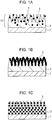
- Figs. 1A to 1C are schematic diagrams illustrating optical members according to an embodiment of the present invention.
- the optical member of the present invention includes an antireflection coating 10 disposed on a substrate 1.
- a crystalline layer 2 having a textured structure containing aluminum oxide crystals is disposed on a substrate 1.
- the textured structure has a large number of protrusions 6 (structure containing aluminum oxide crystals at 50 wt% or more).
- the crystalline layer 2 having a textured structure contains a carboxylic acid compound 3.
- the antireflection coating 10 is constituted of the crystalline layer 2.
- the crystalline layer 2 having a textured structure contains a carboxylic acid compound, which means that part of the crystalline layer 2 having a textured structure contains the carboxylic acid compound or that the entire of the crystalline layer 2 having a textured structure contains the carboxylic acid compound.
- the carboxylic acid compound is scattered on part of the surface of the crystalline layer 2 and/or is present in part of the crystalline layer 2 from the surface toward the substrate 1.
- the carboxylic acid compound may be contained in the entire of the crystalline layer 2 having a textured structure.
- the carboxylic acid compound covers the whole surface layer of the crystalline layer 2 or, as shown in Fig. 1C , the carboxylic acid compound is present in the crystalline layer 2 from the surface toward the substrate 1 to reach the substrate 1.
- the crystalline layer 2 having a textured structure can reduce light reflection occurring on the substrate 1, and the crystalline layer 2 having a textured structure containing a carboxylic acid compound 3 can have characteristics showing a low reflection in a wider wavelength region.
- the crystalline layer having a textured structure used in the present invention is an antireflection coating having a nano structure of a certain material and having an apparent refractive index that is lower than the inherent refractive index of the material and varies in the thickness direction of the coating.
- the material can be aluminum oxide.
- the low reflection characteristics are realized by a fine structure having a smaller size than the wavelength used in an optical component to which the antireflection coating is applied.
- the fine structure includes a plurality of closed spaces closed from the outside atmosphere or a plurality of open spaces opened to the outside atmosphere.
- the refractive index (the inherent refractive index) of the material constituting the antireflection coating and the refractive index of the medium such as the air occupying (filling) the spaces are averaged.
- the antireflection coating has a refractive index lower than the refractive index (inherent refractive index) of the material constituting the antireflection coating.
- the apparent refractive index of the antireflection coating can be reduced.
- the inherent refractive index of a material is the refractive index of a non-porous thin coating or balk of the material
- the apparent refractive index is the refractive index reduced by means of the spaces formed in a coating having a fine structure.
- the apparent refractive index can be changed by varying the occupancy rate of the spaces or the occupancy rate of the solid portions in the coating in the thickness direction.
- Fig. 7 is a diagram schematically illustrating a cross section of an antireflection coating used in the present invention.
- the antireflection coating includes solid portions (protrusions) 6 and spaces 11.
- the apparent refractive index can be intermittently or continuously increased from the incidence side of light along the light travelling direction (direction of the arrow A). Alternatively, the apparent refractive index can be intermittently or continuously decreased from the incidence side of light along the light travelling direction (direction of the arrow B).
- the antireflection coating can have optical characteristics such that the outermost surface being in contact with the outer atmosphere of the antireflection coating has a refractive index of approximately 1 and that the refractive index gradually increases along the depth from the outermost surface in the coating thickness direction of the antireflection coating so as to approximate the inherent refractive index (e.g., 1.4 to 3.0) of the material constituting the antireflection coating.
- the inherent refractive index e.g., 1.4 to 3.0
- the antireflection coating may have a structure formed by stacking at least two layers having fine structures of which occupancy rates of the spaces or solid portions are different from each other or may have a structure having a space or solid portion distribution such that the occupancy rate thereof varies.
- the spaces communicate with the outside atmosphere to provide an unsmooth fine textured structure.
- the height (h) of the convex portion (protrusion) is smaller than the wavelength used and specifically is in a nano-order size.
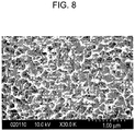
- Such a fine textured structure is expressed as a moth eye structure, sub-wavelength structure (SWS), sponge-like structure, petaloid structure, fabric structure, spiny structure, or beard-like structure (see Figs. 7 and 8 and Japanese Patent Laid-Open Nos. 09-202649 , 2005-275372 , and 2006-259711 ).
- Fig. 8 is an electron micrograph of the surface of an optical member according to an embodiment of the present invention.
- Examples of the material used in the solid portion include metal oxides such as silicon oxide, zinc oxide, titanium oxide, magnesium oxide, zirconium oxide, and aluminum oxide; metal fluorides such as magnesium fluoride; metal compounds such as metal fluoride oxides and metal hydroxides; and those containing them.
- the metal element is not limited to one type, and a metal compound of multi-element system, i.e., a binary or ternary compound system, can also be used.
- these solid materials may contain, for example, phosphorus or boron.
- the crystalline structure of the solid portion is not particularly limited and may be amorphous, fine crystalline, polycrystalline, or monocrystalline or an amorphous structure containing these crystals.
- the antireflection coating is produced by forming a solid coating by vacuum deposition, sputtering, a gas phase method represented by CVD, or a liquid phase method such as a sol-gel method, a coating method, or spraying and subjecting the solid coating to a surface treatment such as heat treatment or hot-water treatment to form a fine textured structure (protrusions) on the surface.
- an amorphous aluminum oxide coating is formed on a substrate by a sol-gel method, and the coating is brought into contact with hot water or water vapor.
- plate crystals of aluminum oxide which is also called boehmite, aluminum hydroxide, or a hydrate thereof grow to provide a petaloid fine textured structure (protrusions).
- an intermediate layer may be disposed between the antireflection coating having the fine textured structure (protrusions) and the substrate.
- the intermediate layer can be a solid coating having a median refractive index between the apparent refractive index of the antireflection coating and the refractive index of the substrate.
- Specific examples of the material for the intermediate layer include inorganic materials such as metal compounds mentioned as the materials for the antireflection coating and organic materials such as resins represented by polyimide.
- the aluminum oxide crystals constituting the crystalline layer 2 having a textured structure are formed of an oxide or hydroxide of aluminum or a hydrate thereof.
- the crystals can be boehmite.
- These crystals arranged in the crystalline layer 2 form fine protrusions with their edges. Accordingly, the crystals are selectively arranged at a specific angle with respect to the substrate surface for increasing the heights of the protrusions and narrowing the distances between the protrusions.
- Figs. 2A and 2B are schematic diagrams explaining a relationship between a textured structure containing aluminum oxide crystals of the present invention and a substrate.
- the substrate has a flat surface such as a plate, film, or sheet, as shown in Fig. 2A
- the protrusions 6 are arranged with respect to the substrate such that the average of angles ⁇ 1 between the tilt directions 7 of the protrusions 6 and the substrate surface 8 is 45° or more and 90° or less, such as 60° or more and 90° or less.
- the protrusions 6 are arranged with respect to the substrate such that an average of angles ⁇ 2 between the tilt directions 7 of the protrusions 6 and a tangent 9 to any point on the substrate surface is equal to or greater than 45° and equal to or less than 90°.
- the average of angles ⁇ 2 between the tilt directions 7 of the protrusions 6 and the tangent 9 to any point on the substrate may be between 60° and 90° including both 60° and 90°.
- the angles ⁇ 1 and ⁇ 2 may exceed 90° depending on the tilt of a protrusion 6. In such a case, the angle measured so as to be 90° or less is used.
- the thickness of the crystalline layer 2 having a textured structure can be 20 nm or more and 1000 nm or less.
- the thickness may be range between 50 nm and 1000 nm.
- the antireflection performance by the textured structure is effective, the protrusions do not have a risk of impairing their mechanical strength, and such a thickness is advantageous for the manufacturing cost of the textured structure.
- a thickness of 50 nm or more and 1000 nm or less can further enhance the antireflection performance.
- the surface density of the textured structure is also important, and the average surface roughness Ra' value, which corresponds to the surface density and is obtained by planar extension of the center line average roughness, can be 5 nm or more, such as 10 nm or more, and particularly 15 nm or more and 100 nm or less.
- the surface area ratio S r is 1.1 or more, such as 1.15 or more, and particularly 1.2 or more and 3.5 or less.
- the textured structure When the surface density of a textured structure has an Ra' of 5 nm or more and an Sr of 1.1 or more, the textured structure can exhibit an antireflection effect.
- the antireflection effect In the case of an Ra' of 10 nm or more and an S r of 1.15 or more, the antireflection effect is higher than that of the former, and in the case of an Ra' of 15 nm or more and an S r of 1.2 or more, the antireflection performance becomes a level that can be actually used.
- the scattering effect by the textured structure is higher than the antireflection effect thereof, resulting in insufficient antireflection performance.
- the carboxylic acid compound 3 of the present invention can have a high affinity to aluminum oxide constituting the crystalline layer 2 having a textured structure or can be present in the state where its carboxyl groups of the carboxylic acid compound are conjugated.
- the carboxylic acid compound can be present as a carboxylate with aluminum oxide constituting the crystalline layer 2 having a textured structure and/or in a state of carboxylic acid compound molecules coupled with each other and/or as a free carboxylic acid compound without coupling with other molecules.
- the carboxylic acid compound 3 present in the above-mentioned states in the crystalline layer 2 having a textured structure causes a slight change in the electronic state of the crystalline layer 2 having a textured structure. This is believed to slightly change the refractive index structure of the crystalline layer 2 having a textured structure and thereby decrease the reflectance in a wide wavelength region compared with the case where the crystalline layer 2 having a textured structure does not contain the carboxylic acid compound 3.
- the crystalline layer 2 having a textured structure is constituted of crystals mainly composed of an oxide or hydroxide of aluminum or a hydrate thereof. Accordingly, it is believed that the carboxylic acid acts on the hydroxyl group or the hydrate binding to aluminum to form a metastable state such as an ionic bond or a coordinate bond. That is, it is believed that carboxylates are formed between part or the entire of the crystalline layer 2 having a textured structure and part or the entire of the carboxylic acid compound 3 to enhance the chemical stability of the crystalline layer 2 having a textured structure. This is believed to be caused by that contamination materials are prevented from adsorbing to the textured structure constituted of boehmite formed on the surface layer of aluminum oxide. As a result, an effect of preventing a change over time in refractive index, which is caused by partial deterioration of the fine structure or adsorption of other types of compounds, can be further expressed.
- the free carboxylic acid compound present in part or the entire of the crystalline layer 2 having a textured structure is similarly expected to be formed into a metastable carboxylate against the instability of the aluminum oxide due to a change in environment.
- carboxylic acid compound examples include monovalent to multivalent linear saturated or unsaturated hydrocarbon carboxylic acid compounds, monovalent to multivalent cyclic saturated or unsaturated hydrocarbon carboxylic acid compounds, and monovalent to multivalent aromatic carboxylic acid compounds.
- carboxylic acid compound examples include oxalic acid, malonic acid, succinic acid, glutaric acid, adipic acid, pimelic acid, suberic acid, azelaic acid, sebacic acid, phthalic acid, isophthalic acid, terephthalic acid, polyacrylic acid, meso-2,3-dimercaptosuccinic acid, meso-butane-1,2,3,4-tetracarboxylic acid, tetrahydrofuran-2,3,4,5-tetracarboxylic acid, 1,2,3,4-cyclopentanetetracarboxylic acid, tetrafluorosuccinic acid and fumaric acid.
- carboxylic acid compounds those soluble in water or a solvent miscible with water can be particularly used.
- the use of a carboxylic acid compound having two or more carboxyl groups in one molecule can provide the following three effects: an increase in probability of reaction with an oxide or hydroxide of aluminum or a hydrate thereof mainly constituting the crystalline layer 2 having a textured structure in the production process; an increase in apparent molecular size by hydrogen bonds between carboxylic acid molecules to cause a larger change in the electronic state, which changes the refractive index structure determining reflectance; and an increase in affinity of the carboxylic acid compound to aluminum oxide mainly constituting the crystalline layer 2 having a textured structure when the carboxylic acid compound is added to the crystalline layer 2.
- the carboxylic acid compound can have at least one hydroxyl group in its molecule.
- Examples of the carboxylic acid compound having at least one hydroxyl group include malic acid, tartaric and citric acid.
- the hydroxyl group is believed to further effectively acts in the effects described in the compound having two or more carboxyl groups in the molecule.
- These carboxylic acid compounds may be used in combination of two or more thereof from the viewpoints of changes in reflectance and shape in the production process and changes in optical characteristics under various environments.
- the method of producing the optical member according to the present invention produces an optical member having an antireflection coating disposed on a substrate and includes the following four steps of:
- the aluminum oxide layer containing aluminum oxide can be mainly composed of aluminum oxide, such as an aluminum oxide layer containing aluminum oxide at 50 wt% or more.
- Figs. 3A to 3C are process diagrams showing a method of producing the optical member according to an embodiment of the present invention.
- aluminum oxide crystals refers to crystals precipitating and growing on the surface of a coating containing aluminum oxide through, for example, peptization of the surface layer of the aluminum oxide coating by bringing the coating into contact with hot water or water vapor.
- the crystals are in the form of a fine textured structure.
- crystals having a variety of sizes are randomly arranged, and their top edges form protrusions. Therefore, in order to vary the heights, sizes, and angles of the protrusions and the distance between protrusions, the precipitation and growth of the crystals should be controlled.
- Fig. 3A shows the step (a) of forming an aluminum oxide layer containing aluminum oxide on a substrate. That is, Fig. 3A shows the state where an aluminum oxide layer 5, i.e., a source of the crystalline layer having a fine textured structure constituted of aluminum oxide crystals in the present invention, is disposed on a substrate 1.
- an aluminum oxide layer 5 i.e., a source of the crystalline layer having a fine textured structure constituted of aluminum oxide crystals in the present invention
- the aluminum oxide layer 5 may be formed by applying a coating liquid containing aluminum oxide prepared by, for example, a sol-gel method onto a substrate by spin coating, dip coating, spray coating, etc.
- the aluminum oxide layer 5 may be formed by sputtering or vapor deposition.
- application of a sol-gel coating liquid containing aluminum oxide can be performed.
- drying by heating in an oven with internal air circulation, muffle furnace, or IH furnace or heating with an IR lump may be appropriately performed.
- the aluminum oxide layer may contain an oxide such as TiO 2 , ZrO 2 , SiO 2 , ZnO, or MgO as a different kind of component in the coating containing aluminum oxide.
- Fig. 3B shows the step (b) of forming a crystalline layer having a textured structure by bringing the aluminum oxide layer into contact with hot water or water vapor.
- Aluminum oxide crystals are formed by bringing the surface of the aluminum oxide coating into contact with hot water.
- the temperature of the hot water is in the range of 60°C or more and 100°C or less, and the coating is immersed in hot water for 5 minutes to 24 hours and is then dried.
- an amorphous aluminum oxide layer may remain under the crystalline layer 2 having a textured structure.
- a plate crystal layer having a textured structure containing aluminum oxide crystals on the surface by bringing an amorphous coating containing aluminum oxide into contact with hot water or water vapor can be performed by the process described in, for example, Japanese Patent Laid-Open No. 2006-259711 or 2005-275372 .
- Fig. 3C shows the step (c) of applying a coating liquid containing a carboxylic acid compound and a solvent onto the crystalline layer and the step (d) of removing the solvent of the coating liquid, i.e., the state where a carboxylic acid compound 3 in the present invention is disposed on part of the crystalline layer 2 having a textured structure.
- the coating liquid containing the carboxylic acid compound is prepared by dissolving the above-mentioned carboxylic acid compound in a solvent in a concentration of 0.001 to 10 wt% or of 0.1 mM to 10 M.
- the amount of the carboxylic acid compound is determined in light of the desired reflectance or changes under various environments. A too large amount prevents realization of functions as an antireflection coating, and a too small amount cannot inhibit changes under a high-temperature and high humidity environment.
- the solvent can be water.
- the solvent may be a highly hydrophilic solvent or an alcohol, diol, glycol, or ether solvent. These solvents may be used in combination from the viewpoints of coating properties and easiness in removal of the solvent described below.
- the coating liquid containing carboxylic acid is applied onto the crystalline layer 2 having a textured structure by a method such as spin coating, dip coating, or spray coating. Subsequently, the solvent contained in the coating liquid is removed. Examples of the method of removing the solvent include a method of heating in an oven with internal air circulation, muffle furnace, or IH furnace or heating with an IR lump.
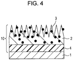
- the optical member of the present invention may have a refractive index ni layer 4 between the substrate 1 and the crystalline layer 2 having a textured structure containing aluminum oxide crystals.
- the refractive index difference between the substrate 1 and the crystalline layer 2 having a textured structure can be adjusted by providing the refractive index ni layer 4.
- the method of producing the optical member of the present invention may include a step of forming a refractive index layer before the formation of the aluminum oxide layer.
- Fig. 4 shows an example of the optical member having a refractive index ni layer 4 between the substrate 1 and the crystalline layer 2 having a textured structure containing aluminum oxide crystals.
- the antireflection coating 10 on the substrate 1 is constituted of a refractive index ni layer 4 and a crystalline layer 2.
- the refractive index nb of the substrate, the refractive index ni of the refractive index ni layer, and the refractive index ns of the crystalline layer having a textured structure containing aluminum oxide crystals can satisfy a relationship of nb > ni > ns.
- the refractive index ni layer 4 can be a transparent coating made of an inorganic material or an organic material.
- Examples of the inorganic material include metal oxides such as SiO 2 , TiO 2 , ZrO 2 , ZnO, and Ta 2 O 5 .
- Examples of the method of forming the refractive index ni layer 4 from an inorganic material include vacuum deposition such as vapor deposition and sputtering and a sol-gel method by application of a metal oxide precursor sol.
- organic material examples include acrylic resins, epoxy resins, oxetane resins, maleimide resins, melamine resins, benzoguanamine resins, phenol resins, resol resins, and polymers such as polycarbonate, polyester, polyacrylate, polyether, polyurea, polyurethane, polyamide, polyamide imide, polyimide, polyketone, polysulfone, polyphenylene, polyxylene, and polycycloolefin.
- acrylic resins epoxy resins, oxetane resins, maleimide resins, melamine resins, benzoguanamine resins, phenol resins, resol resins
- polymers such as polycarbonate, polyester, polyacrylate, polyether, polyurea, polyurethane, polyamide, polyamide imide, polyimide, polyketone, polysulfone, polyphenylene, polyxylene, and polycycloolefin.
- Formation of the refractive index ni layer 4 from an organic material is mainly performed by, for example, wet coating by application of a solution containing the organic material.
- a drying step may be appropriately performed.
- Examples of the substrate used in the present invention include glass, plastic substrates, glass mirrors, and plastic mirrors.
- the glass include alkali-containing glass, alkali-free glass, aluminosilicate glass, borosilicate glass, barium based glass, and lanthanum based glass.
- plastic substrate examples include films and molded products of thermoplastic resins such as polyester, triacetyl cellulose, cellulose acetate, polyethylene terephthalate, polypropylene, polystyrene, polycarbonate, polymethyl methacrylate, ABS resins, polyphenylene oxide, polyurethane, polyethylene, and polyvinyl chloride; and cross-linking films and crosslinked molded products prepared from various thermoplastic resins such as unsaturated polyester resins, phenol resins, cross-linking polyurethane, cross-linking acrylic resins, and cross-linking saturated polyester resins.
- thermoplastic resins such as polyester, triacetyl cellulose, cellulose acetate, polyethylene terephthalate, polypropylene, polystyrene, polycarbonate, polymethyl methacrylate, ABS resins, polyphenylene oxide, polyurethane, polyethylene, and polyvinyl chloride
- cross-linking films and crosslinked molded products prepared from various thermoplastic resins such as unsaturated
- the substrate may have any shape as long as a shape according to the purpose of use can be eventually provided, and a flat plate, film, or a sheet is used as the substrate.
- the substrate may have a two-dimensional or three-dimensional curved surface.
- Each of a series of flat circular substrates made of a glass base material having a diameter of about 30 mm and a thickness of about 2 mm was polished on one side, ultrasonic washed with an alkali detergent and IPA, and then dried in an oven.
- a solution of 0.01 M diluted hydrochloric acid in a solvent mixture of 2-ethylbutanol and 1-ethoxy-2-propanol was slowly added to the aluminum-sec-butoxide solution prepared above in an amount of 1.5 molar equivalents based on the amount of the aluminum-sec-butoxide, followed by stirring for a while.
- the amounts of the solvents were adjusted such that the final amount of the aluminum-sec-butoxide was 18.7 wt% and the mixture ratio of 2-ethylbutanol to 1-ethoxy-2-propanol was 7/3.
- the resulting solution was used as a precursor sol liquid for forming an aluminum oxide layer.
- the solution was stirred at room temperature for 15 hours for polymerization.
- the resulting solution was diluted with DMAc to 8 wt%, and 7.4 g of pyridine and 3.8 g of acetic anhydride were added thereto, followed by stirring at room temperature for 1 hour and then in an oil bath with heating at 70°C for 4 hours.
- the resulting polymer solution was reprecipitated in methanol to extract the polymer.
- the polymer was washed in methanol several times and was then dried in vacuum at 100°C to yield 5.9 g of polyimide as a light yellow powder.
- the remaining quantity of carboxyl groups was determined from the 1 H-NMR spectrum to confirm an imidization ratio of 99%.
- Aqueous carboxylic acid solutions containing carboxylic acid compounds at concentrations shown in Table 1 were prepared using deionized water.
- Reflectance was measured at an incident angle of 0° of light in the wavelength range of 400 to 700 nm with an absolute reflectance measurement apparatus (USPM-RU, manufactured by Olympus Corp.). The average of reflectances in the wavelength range of 400 to 700 nm was defined as an average reflectance.
- Coating thicknesses and refractive indices were measured in the wavelength range of 380 to 800 nm with a spectroscopic ellipsometer (VASE, manufactured by J. A. Woollam Japan, Co., Inc.).
- the substrate surface was treated with Pd/Pt, and the surface was observed at an accelerating voltage of 2 kV using a field emission scanning electron microscope (FE-SEM) (S-4800, manufactured by Hitachi High-Technologies Corp.).
- FE-SEM field emission scanning electron microscope
- a high-temperature high-humidity accelerated test was performed by leaving test samples in a small size environmental tester (SH-241, manufactured by Espec Corporation) under environments of a temperature of 75°C and a humidity of 90% for 12 hours.
- SH-241 manufactured by Espec Corporation
- a crystalline layer 2 having a textured structure was produced on a Si wafer substrate. Subsequently, the crystalline layer 2 was treated so as to contain a carboxylic acid compound.
- the substrate was subjected to Fourier transform infrared spectroscopy (hereinafter, referred to as FT-IR, FTS7000e manufactured by Varian, Inc., USA) in the wavenumber of 450 to 4000 cm -1 to confirm the peak of the carboxylic acid.
- FT-IR Fourier transform infrared spectroscopy
- This substrate was dried at 200°C for 60 minutes to provide a substrate having a refractive index ni layer 4.
- the thickness and the refractive index of the resulting refractive index ni layer 4 were measured with a spectroscopic ellipsometer.
- the thickness was 48 nm, and the refractive index n was 1.62.
- An appropriate amount of the aluminum oxide precursor sol was dropped onto the surface of the refractive index ni layer 4, followed by spin coating at 4000 rpm for 20 seconds and then baking in an oven with internal air circulation at 200°C for 120 minutes.
- the refractive index ni layer 4 was covered with an amorphous aluminum oxide coating.
- the thickness and the refractive index of the resulting amorphous aluminum oxide coating were measured with an ellipsometer.
- the thickness was 150 nm, and the refractive index n was 1.50.
- the substrate was immersed in hot water of 75°C for 20 minutes and was then dried at 60°C for 15 minutes.
- the absolute reflectance of the antireflection coating on the glass A was measured.
- the surfaces of a part of the produced samples were investigated with an FE-SEM, and textured structures of crystals mainly composed of aluminum oxide formed randomly and intricately were observed.
- the absolute reflectance of the antireflection coating on the glass A was measured. It was confirmed that the glass substrate provided with an antireflection coating having an absolute reflectance of 0.1% or less in the wavelength range of 400 to 700 nm was prepared.
- the reflectance after production of the crystalline layer 2 having a textured structure was compared with the reflectance after spin coating of the aqueous carboxylic acid compound solution and baking. As shown in Table 2, it was recognized that the reflectance was reduced in the wavelength range of 400 to 700 nm, in particular, significantly reduced on the shorter wavelength side.
- Fig. 5A is a graph showing absolute reflectances in the wavelength range of 400 to 700 nm of an antireflection coating formed on glass A in Example 5.
- the short dashed line shows the reflectance after immersion in hot water and drying but before carboxylic acid compound treatment, and the solid line shows the reflectance after carboxylic acid compound treatment.
- the optical coating on the glass A was subjected to a high-temperature high-humidity accelerated test.
- the results are shown in Table 3.
- the amounts of variation of the reflectance at wavelengths of 400, 550, and 700 nm were small.
- the long dashed line in Fig. 5A shows the actual measurement data of reflectance after the high-temperature high-humidity accelerated test in Example 5.
- a high-temperature high-humidity accelerated test was performed as in Examples 1 to 5 to confirm the amounts of variation of the reflectance at wavelengths of 400, 550, and 700 nm. The results are shown in Table 3. The amount of variation of the reflectance highly varied to show insufficient antireflection performance.
- Fig. 5B shows the actual measurement data of reflectance in Comparative Example 1. The solid line shows the reflectance after immersion in hot water and drying but before the high-temperature high-humidity accelerated test, and the long dashed line shows the reflectance after the high-temperature high-humidity accelerated test.
- Table 1 Aqueous carboxylic acid solution Carboxylic acid compound Manufacturer Concentration aqueous carboxylic acid solution 1 meso-butane-1,2,3,4-tetracarboxylic acid Tokyo Chemical Industry Co., Ltd. 0.075 wt% aqueous carboxylic acid solution 2 tetrahydrofuran-2,3,4,5-tetracarboxylic acid Tokyo Chemical Industry Co., Ltd. 0.075 wt% aqueous carboxylic acid solution 3 1,2,3,4-cyclopentanetetracarboxylic acid Tokyo Chemical Industry Co., Ltd. 0.075 wt% aqueous carboxylic acid solution 4 phthalic acid Tokyo Chemical Industry Co., Ltd.
- Example 6 aqueous carboxylic acid compound solution 5 was used, and the same process as that in Examples 1 to 5 was conducted except that the step of forming the refractive index ni layer 4 was omitted.
- the reflectance after the treatment with aqueous carboxylic acid compound solution 5 decreased in the wavelength range of 400 to 700 nm.
- the results are shown in Table 2 and Fig. 6A .
- the short dashed line shows the reflectance after immersion in hot water and drying but before carboxylic acid compound treatment, and the solid line shows the reflectance after carboxylic acid compound treatment.
- Example 6 The same process as that in Example 6 was conducted except that application of the aqueous carboxylic acid compound solution 5 and baking were omitted.
- a high-temperature high-humidity accelerated test was performed.
- the amounts of variation of the reflectance at wavelengths of 400, 550, and 700 nm were large to show insufficient antireflection performance.
- Fig. 6B shows the actual measurement data of reflectance in Comparative Example 4.
- the solid line shows the reflectance after immersion in hot water and drying but before the high-temperature high-humidity accelerated test, and the long dashed line shows the reflectance after the high-temperature high-humidity accelerated test.
- the optical member of the present invention has high antireflection performance and therefore can be utilized in an image pickup optical system used in a photographing lens such as a camera, a projection optical system used in, for example, a projector, or an observation optical system used in, for example, binoculars.
Landscapes
- Chemical & Material Sciences (AREA)
- Physics & Mathematics (AREA)
- Engineering & Computer Science (AREA)
- General Physics & Mathematics (AREA)
- Optics & Photonics (AREA)
- Chemical Kinetics & Catalysis (AREA)
- Organic Chemistry (AREA)
- Materials Engineering (AREA)
- General Chemical & Material Sciences (AREA)
- Inorganic Chemistry (AREA)
- Thermal Sciences (AREA)
- Mechanical Engineering (AREA)
- Metallurgy (AREA)
- Life Sciences & Earth Sciences (AREA)
- Geochemistry & Mineralogy (AREA)
- Crystallography & Structural Chemistry (AREA)
- Ceramic Engineering (AREA)
- Surface Treatment Of Optical Elements (AREA)
- Laminated Bodies (AREA)
Claims (6)
- Optisches Element umfassend eine auf einem Substrat (1) angeordnete Antireflexionsbeschichtung (10), wobeidie Antireflexionsbeschichtung (10) eine äußerste Schicht aufweist, welche eine kristalline Schicht (2) mit einer Aluminiumoxidkristalle beinhaltenden texturierten Struktur ist, wobei die texturierte Struktur eine Nanostruktur mit einem offenbaren Brechungsindex ist, welcher niedriger ist als der inhärente Brechungsindex des Materials der Nanostruktur und welcher in der Dickenrichtung der Beschichtung variiert,dadurch gekennzeichnet, dassdie kristalline Schicht (2) weiterhin eine Carbonsäureverbindung (3) beinhaltet, welche zwei oder mehr Carboxygruppen in einem Molekül aufweist.
- Optisches Element nach Anspruch 1, wobei die Carbonsäureverbindung (3) zusätzlich zu den Carboxygruppen zumindest eine Hydroxylgruppe im Molekül aufweist.
- Optisches Element nach Anspruch 1 oder 2, weiter umfassend eine Brechungsindexschicht (4) zwischen dem Substrat (1) und der kristallinen Schicht (2), wobeider Brechungsindex nb des Substrats (1), der Brechungsindex ni der Brechungsindexschicht (4) und der Brechungsindex ns der kristallinen Schicht (2) mit der Aluminiumoxidkristalle beinhaltenden texturierten Struktur eine Beziehung nb > ni > ns erfüllen.
- Optisches Element nach Anspruch 1, wobei die Carbonsäureverbindung (3) Meso-Butan-1,2,3,4-Tetracarbonsäure, Tetrahydrofuran-2,3,4,5-Tetracarbonsäure, 1,2,3,4-Cyclopentantetracarbonsäure, Phthalsäure oder Zitronensäure ist.
- Verfahren zum Herstellen eines optischen Elements mit einer Antireflexionsbeschichtung (10) auf einem Substrat (1), wobei das Verfahren umfasst:(a) Bilden einer Aluminiumoxid beinhaltenden Aluminiumoxidschicht (5) auf einem Substrat (1); und(b) Bilden einer kristallinen Schicht (2) mit einer texturierten Struktur durch In-Kontakt-Bringen der Aluminiumoxidschicht mit heißem Wasser von 60°C oder mehr und 100°C oder weniger, wobei die texturierte Struktur eine Nanostruktur mit einem offenbaren Brechungsindex ist, welcher niedriger ist als der inhärente Brechungsindex des Materials der Nanostruktur und welcher in der Dickenrichtung der Beschichtung variiert,gekennzeichnet durch weiter umfassend:(c) Aufbringen einer Beschichtungsflüssigkeit, die eine Carbonsäureverbindung (3) beinhaltet, welche zwei oder mehr Carboxygruppen in einem Molekül aufweist, sowie eines Lösungsmittels auf die kristalline Schicht (2); und(d) Entfernen des Lösungsmittels der Beschichtungsflüssigkeit.
- Verfahren zum Herstellen eines optischen Elements nach Anspruch 5, weiter umfassend das Bilden einer Brechungsindexschicht (4) auf dem Substrat (1), wobeidie Aluminiumoxid beinhaltende Aluminiumoxidschicht (5) auf der Brechungsindexschicht (4) gebildet wird.
Applications Claiming Priority (1)
| Application Number | Priority Date | Filing Date | Title |
|---|---|---|---|
| JP2012077502 | 2012-03-29 |
Publications (2)
| Publication Number | Publication Date |
|---|---|
| EP2645136A1 EP2645136A1 (de) | 2013-10-02 |
| EP2645136B1 true EP2645136B1 (de) | 2017-01-18 |
Family
ID=47996965
Family Applications (1)
| Application Number | Title | Priority Date | Filing Date |
|---|---|---|---|
| EP13001164.6A Not-in-force EP2645136B1 (de) | 2012-03-29 | 2013-03-08 | Optisches Element mit texturierter Struktur und Verfahren zu dessen Herstellung |
Country Status (4)
| Country | Link |
|---|---|
| US (1) | US20130260096A1 (de) |
| EP (1) | EP2645136B1 (de) |
| JP (1) | JP6207199B2 (de) |
| CN (1) | CN103364848B (de) |
Families Citing this family (23)
| Publication number | Priority date | Publication date | Assignee | Title |
|---|---|---|---|---|
| US20140252619A1 (en) * | 2013-03-08 | 2014-09-11 | Taiwan Semiconductor Manufacturing Company, Ltd. | Interconnect structure that avoids insulating layer damage and methods of making the same |
| JP6502021B2 (ja) * | 2013-04-10 | 2019-04-17 | デクセリアルズ株式会社 | 位相差補償素子及び投射型画像投影装置 |
| WO2015080030A1 (en) * | 2013-11-27 | 2015-06-04 | Canon Kabushiki Kaisha | Optical member and method for manufacturing the same |
| JP2015114381A (ja) * | 2013-12-09 | 2015-06-22 | 東京エレクトロン株式会社 | 反射防止機能を有する部材およびその製造方法 |
| JP2015184404A (ja) * | 2014-03-24 | 2015-10-22 | 富士フイルム株式会社 | 接触検知センサおよび接触検知方法 |
| JP6362105B2 (ja) * | 2014-08-27 | 2018-07-25 | キヤノン株式会社 | 反射防止膜を有する光学素子、光学系、光学機器 |
| CN106062585A (zh) * | 2014-09-25 | 2016-10-26 | 松下知识产权经营株式会社 | 光学构件、该光学构件的制造方法以及摄像装置 |
| EP3026469B1 (de) * | 2014-11-27 | 2023-01-11 | Canon Kabushiki Kaisha | Optisches element und verfahren zur herstellung des optischen elements |
| CN107092044A (zh) * | 2016-09-14 | 2017-08-25 | 上海天臣防伪技术股份有限公司 | 减反射薄膜及其制备方法、其模具的制备方法 |
| JP7119317B2 (ja) | 2016-11-28 | 2022-08-17 | 株式会社リコー | 情報処理装置、撮像装置、機器制御システム、移動体、情報処理方法、及び、情報処理プログラム |
| MY199830A (en) * | 2016-11-28 | 2023-11-23 | Ricoh Co Ltd | Information processing apparatus, imaging apparatus, apparatus control system, movable object, information processing method, and information processing program |
| US20180363125A1 (en) * | 2017-06-20 | 2018-12-20 | Board Of Trustees Of The University Of Arkansas | Method of forming high surface area metal oxide nanostructures and applications of same |
| EP3459353B1 (de) * | 2017-09-26 | 2022-04-20 | Sharp Kabushiki Kaisha | Synthetischer polymerfilm dessen oberfläche eine mikrobizide wirkung aufweist, lichthärtbare harzzusammensetzung, herstellungsverfahren eines synthetischen polymerfilms, und sterilisationsverfahren durch verwendung einer oberfläche eines synthetischen polymerfilms |
| US11105960B2 (en) * | 2017-12-19 | 2021-08-31 | Canon Kabushiki Kaisha | Optical element and method of producing the element, and optical instrument |
| JP7378924B2 (ja) * | 2017-12-19 | 2023-11-14 | キヤノン株式会社 | 光学素子、その製造方法、撮像装置、および光学機器 |
| US12411307B2 (en) | 2020-12-23 | 2025-09-09 | Largan Precision Co., Ltd. | Optical lens assembly, imaging apparatus and electronic device |
| US12235409B2 (en) | 2020-12-23 | 2025-02-25 | Largan Precision Co., Ltd. | Optical lens assembly, imaging apparatus and electronic device |
| US12379524B2 (en) | 2021-09-01 | 2025-08-05 | Largan Precision Co., Ltd. | Optical imaging lens assembly comprising a gradient refractive coating having a plurality of holes, imaging apparatus and electronic device |
| TWI821864B (zh) * | 2021-12-29 | 2023-11-11 | 大立光電股份有限公司 | 成像鏡頭、遮光片及電子裝置 |
| TWI831649B (zh) | 2023-03-03 | 2024-02-01 | 大立光電股份有限公司 | 成像鏡頭、相機模組與電子裝置 |
| FI20235855A1 (en) * | 2023-08-01 | 2025-02-02 | Teknologian Tutkimuskeskus Vtt Oy | Anti-reflective treated surface and method for manufacturing it |
| FI20245571A1 (en) * | 2024-05-08 | 2025-11-09 | Beneq Oy | An anti-reflective coating on a surface of a substrate |
| WO2025258409A1 (ja) * | 2024-06-14 | 2025-12-18 | Agc株式会社 | 光学フィルタ及び撮像装置 |
Citations (2)
| Publication number | Priority date | Publication date | Assignee | Title |
|---|---|---|---|---|
| GB2112301A (en) * | 1981-12-24 | 1983-07-20 | Nhk Spring Co Ltd | Reflector and method for manufacturing the same |
| US5624604A (en) * | 1994-05-09 | 1997-04-29 | Yasrebi; Mehrdad | Method for stabilizing ceramic suspensions |
Family Cites Families (10)
| Publication number | Priority date | Publication date | Assignee | Title |
|---|---|---|---|---|
| JPH09202649A (ja) | 1996-01-24 | 1997-08-05 | Central Glass Co Ltd | 花弁状透明アルミナ膜及びその形成法 |
| JP4182236B2 (ja) | 2004-02-23 | 2008-11-19 | キヤノン株式会社 | 光学部材および光学部材の製造方法 |
| JP4520418B2 (ja) | 2005-02-18 | 2010-08-04 | キヤノン株式会社 | 光学用透明部材及びそれを用いた光学系 |
| JP4857290B2 (ja) | 2007-01-22 | 2012-01-18 | キヤノン株式会社 | 光学部材及び光学部材の製造方法 |
| JP4639241B2 (ja) * | 2007-02-20 | 2011-02-23 | キヤノン株式会社 | 光学用部材、それを用いた光学系及び光学用部材の製造方法 |
| JP5814512B2 (ja) * | 2009-03-31 | 2015-11-17 | キヤノン株式会社 | 光学用部材、その製造方法及び光学系 |
| RU2519411C1 (ru) * | 2010-03-08 | 2014-06-10 | Шарп Кабусики Кайся | Способ обработки смазкой для пресс-формы, пресс-форма, способ изготовления антиотражающей пленки, устройство для обработки смазкой для пресс-формы и устройство для промывки/просушки пресс-формы |
| WO2011140018A1 (en) * | 2010-05-07 | 2011-11-10 | 3M Innovative Properties Company | Antireflective films comprising microstructured surface |
| US9045651B2 (en) * | 2010-06-22 | 2015-06-02 | University Of Florida Research Foundation, Inc. | Antifouling surfaces, methods of manufacture thereof and articles comprising the same |
| JP2012073590A (ja) * | 2010-08-31 | 2012-04-12 | Canon Inc | 光学部材、その製造方法及び光学系 |
-
2013
- 2013-03-08 EP EP13001164.6A patent/EP2645136B1/de not_active Not-in-force
- 2013-03-13 US US13/799,954 patent/US20130260096A1/en not_active Abandoned
- 2013-03-28 JP JP2013070537A patent/JP6207199B2/ja not_active Expired - Fee Related
- 2013-03-29 CN CN201310106302.2A patent/CN103364848B/zh not_active Expired - Fee Related
Patent Citations (2)
| Publication number | Priority date | Publication date | Assignee | Title |
|---|---|---|---|---|
| GB2112301A (en) * | 1981-12-24 | 1983-07-20 | Nhk Spring Co Ltd | Reflector and method for manufacturing the same |
| US5624604A (en) * | 1994-05-09 | 1997-04-29 | Yasrebi; Mehrdad | Method for stabilizing ceramic suspensions |
Also Published As
| Publication number | Publication date |
|---|---|
| CN103364848A (zh) | 2013-10-23 |
| JP6207199B2 (ja) | 2017-10-04 |
| US20130260096A1 (en) | 2013-10-03 |
| JP2013228728A (ja) | 2013-11-07 |
| CN103364848B (zh) | 2015-08-05 |
| EP2645136A1 (de) | 2013-10-02 |
Similar Documents
| Publication | Publication Date | Title |
|---|---|---|
| EP2645136B1 (de) | Optisches Element mit texturierter Struktur und Verfahren zu dessen Herstellung | |
| JP4182236B2 (ja) | 光学部材および光学部材の製造方法 | |
| US10459125B2 (en) | Optical member, method for manufacturing optical member, and optical film of optical member | |
| JP4520418B2 (ja) | 光学用透明部材及びそれを用いた光学系 | |
| US8084082B2 (en) | Optical member, optical system using the optical member, and method of manufacturing an optical member | |
| US10983253B2 (en) | Optical member and method for manufacturing optical member | |
| US8980401B2 (en) | Optical member and method of producing the same | |
| CN100595608C (zh) | 光学透明部件和使用该光学透明部件的光学系统 | |
| JP6433110B2 (ja) | 光学用部材及びその製造方法 | |
| CN101889218B (zh) | 氧化物膜、用于形成氧化物膜的涂布溶液、使用该氧化物膜的光学部件和该光学部件的制备方法 | |
| JP5535052B2 (ja) | 光学用部材、それを用いた光学系 |
Legal Events
| Date | Code | Title | Description |
|---|---|---|---|
| PUAI | Public reference made under article 153(3) epc to a published international application that has entered the european phase |
Free format text: ORIGINAL CODE: 0009012 |
|
| AK | Designated contracting states |
Kind code of ref document: A1 Designated state(s): AL AT BE BG CH CY CZ DE DK EE ES FI FR GB GR HR HU IE IS IT LI LT LU LV MC MK MT NL NO PL PT RO RS SE SI SK SM TR |
|
| AX | Request for extension of the european patent |
Extension state: BA ME |
|
| 17P | Request for examination filed |
Effective date: 20140318 |
|
| RBV | Designated contracting states (corrected) |
Designated state(s): AL AT BE BG CH CY CZ DE DK EE ES FI FR GB GR HR HU IE IS IT LI LT LU LV MC MK MT NL NO PL PT RO RS SE SI SK SM TR |
|
| 17Q | First examination report despatched |
Effective date: 20150421 |
|
| REG | Reference to a national code |
Ref country code: DE Ref legal event code: R079 Ref document number: 602013016636 Country of ref document: DE Free format text: PREVIOUS MAIN CLASS: G02B0001110000 Ipc: G02B0001118000 |
|
| GRAP | Despatch of communication of intention to grant a patent |
Free format text: ORIGINAL CODE: EPIDOSNIGR1 |
|
| RIC1 | Information provided on ipc code assigned before grant |
Ipc: G02B 1/111 20150101ALI20160713BHEP Ipc: G02B 1/02 20060101ALI20160713BHEP Ipc: G02B 1/118 20150101AFI20160713BHEP Ipc: C03C 17/42 20060101ALI20160713BHEP |
|
| INTG | Intention to grant announced |
Effective date: 20160805 |
|
| GRAS | Grant fee paid |
Free format text: ORIGINAL CODE: EPIDOSNIGR3 |
|
| GRAA | (expected) grant |
Free format text: ORIGINAL CODE: 0009210 |
|
| AK | Designated contracting states |
Kind code of ref document: B1 Designated state(s): AL AT BE BG CH CY CZ DE DK EE ES FI FR GB GR HR HU IE IS IT LI LT LU LV MC MK MT NL NO PL PT RO RS SE SI SK SM TR |
|
| RAP1 | Party data changed (applicant data changed or rights of an application transferred) |
Owner name: CANON KABUSHIKI KAISHA |
|
| REG | Reference to a national code |
Ref country code: GB Ref legal event code: FG4D |
|
| REG | Reference to a national code |
Ref country code: CH Ref legal event code: EP |
|
| REG | Reference to a national code |
Ref country code: AT Ref legal event code: REF Ref document number: 863224 Country of ref document: AT Kind code of ref document: T Effective date: 20170215 |
|
| REG | Reference to a national code |
Ref country code: IE Ref legal event code: FG4D |
|
| REG | Reference to a national code |
Ref country code: DE Ref legal event code: R096 Ref document number: 602013016636 Country of ref document: DE |
|
| REG | Reference to a national code |
Ref country code: NL Ref legal event code: MP Effective date: 20170118 |
|
| REG | Reference to a national code |
Ref country code: LT Ref legal event code: MG4D |
|
| REG | Reference to a national code |
Ref country code: AT Ref legal event code: MK05 Ref document number: 863224 Country of ref document: AT Kind code of ref document: T Effective date: 20170118 |
|
| PG25 | Lapsed in a contracting state [announced via postgrant information from national office to epo] |
Ref country code: NL Free format text: LAPSE BECAUSE OF FAILURE TO SUBMIT A TRANSLATION OF THE DESCRIPTION OR TO PAY THE FEE WITHIN THE PRESCRIBED TIME-LIMIT Effective date: 20170118 |
|
| PG25 | Lapsed in a contracting state [announced via postgrant information from national office to epo] |
Ref country code: FI Free format text: LAPSE BECAUSE OF FAILURE TO SUBMIT A TRANSLATION OF THE DESCRIPTION OR TO PAY THE FEE WITHIN THE PRESCRIBED TIME-LIMIT Effective date: 20170118 Ref country code: NO Free format text: LAPSE BECAUSE OF FAILURE TO SUBMIT A TRANSLATION OF THE DESCRIPTION OR TO PAY THE FEE WITHIN THE PRESCRIBED TIME-LIMIT Effective date: 20170418 Ref country code: IS Free format text: LAPSE BECAUSE OF FAILURE TO SUBMIT A TRANSLATION OF THE DESCRIPTION OR TO PAY THE FEE WITHIN THE PRESCRIBED TIME-LIMIT Effective date: 20170518 Ref country code: HR Free format text: LAPSE BECAUSE OF FAILURE TO SUBMIT A TRANSLATION OF THE DESCRIPTION OR TO PAY THE FEE WITHIN THE PRESCRIBED TIME-LIMIT Effective date: 20170118 Ref country code: GR Free format text: LAPSE BECAUSE OF FAILURE TO SUBMIT A TRANSLATION OF THE DESCRIPTION OR TO PAY THE FEE WITHIN THE PRESCRIBED TIME-LIMIT Effective date: 20170419 Ref country code: LT Free format text: LAPSE BECAUSE OF FAILURE TO SUBMIT A TRANSLATION OF THE DESCRIPTION OR TO PAY THE FEE WITHIN THE PRESCRIBED TIME-LIMIT Effective date: 20170118 |
|
| PG25 | Lapsed in a contracting state [announced via postgrant information from national office to epo] |
Ref country code: PT Free format text: LAPSE BECAUSE OF FAILURE TO SUBMIT A TRANSLATION OF THE DESCRIPTION OR TO PAY THE FEE WITHIN THE PRESCRIBED TIME-LIMIT Effective date: 20170518 Ref country code: PL Free format text: LAPSE BECAUSE OF FAILURE TO SUBMIT A TRANSLATION OF THE DESCRIPTION OR TO PAY THE FEE WITHIN THE PRESCRIBED TIME-LIMIT Effective date: 20170118 Ref country code: BG Free format text: LAPSE BECAUSE OF FAILURE TO SUBMIT A TRANSLATION OF THE DESCRIPTION OR TO PAY THE FEE WITHIN THE PRESCRIBED TIME-LIMIT Effective date: 20170418 Ref country code: SE Free format text: LAPSE BECAUSE OF FAILURE TO SUBMIT A TRANSLATION OF THE DESCRIPTION OR TO PAY THE FEE WITHIN THE PRESCRIBED TIME-LIMIT Effective date: 20170118 Ref country code: ES Free format text: LAPSE BECAUSE OF FAILURE TO SUBMIT A TRANSLATION OF THE DESCRIPTION OR TO PAY THE FEE WITHIN THE PRESCRIBED TIME-LIMIT Effective date: 20170118 Ref country code: RS Free format text: LAPSE BECAUSE OF FAILURE TO SUBMIT A TRANSLATION OF THE DESCRIPTION OR TO PAY THE FEE WITHIN THE PRESCRIBED TIME-LIMIT Effective date: 20170118 Ref country code: LV Free format text: LAPSE BECAUSE OF FAILURE TO SUBMIT A TRANSLATION OF THE DESCRIPTION OR TO PAY THE FEE WITHIN THE PRESCRIBED TIME-LIMIT Effective date: 20170118 Ref country code: AT Free format text: LAPSE BECAUSE OF FAILURE TO SUBMIT A TRANSLATION OF THE DESCRIPTION OR TO PAY THE FEE WITHIN THE PRESCRIBED TIME-LIMIT Effective date: 20170118 |
|
| REG | Reference to a national code |
Ref country code: DE Ref legal event code: R097 Ref document number: 602013016636 Country of ref document: DE |
|
| PG25 | Lapsed in a contracting state [announced via postgrant information from national office to epo] |
Ref country code: CZ Free format text: LAPSE BECAUSE OF FAILURE TO SUBMIT A TRANSLATION OF THE DESCRIPTION OR TO PAY THE FEE WITHIN THE PRESCRIBED TIME-LIMIT Effective date: 20170118 Ref country code: SK Free format text: LAPSE BECAUSE OF FAILURE TO SUBMIT A TRANSLATION OF THE DESCRIPTION OR TO PAY THE FEE WITHIN THE PRESCRIBED TIME-LIMIT Effective date: 20170118 Ref country code: RO Free format text: LAPSE BECAUSE OF FAILURE TO SUBMIT A TRANSLATION OF THE DESCRIPTION OR TO PAY THE FEE WITHIN THE PRESCRIBED TIME-LIMIT Effective date: 20170118 Ref country code: IT Free format text: LAPSE BECAUSE OF FAILURE TO SUBMIT A TRANSLATION OF THE DESCRIPTION OR TO PAY THE FEE WITHIN THE PRESCRIBED TIME-LIMIT Effective date: 20170118 Ref country code: EE Free format text: LAPSE BECAUSE OF FAILURE TO SUBMIT A TRANSLATION OF THE DESCRIPTION OR TO PAY THE FEE WITHIN THE PRESCRIBED TIME-LIMIT Effective date: 20170118 |
|
| REG | Reference to a national code |
Ref country code: CH Ref legal event code: PL |
|
| PLBE | No opposition filed within time limit |
Free format text: ORIGINAL CODE: 0009261 |
|
| STAA | Information on the status of an ep patent application or granted ep patent |
Free format text: STATUS: NO OPPOSITION FILED WITHIN TIME LIMIT |
|
| PG25 | Lapsed in a contracting state [announced via postgrant information from national office to epo] |
Ref country code: DK Free format text: LAPSE BECAUSE OF FAILURE TO SUBMIT A TRANSLATION OF THE DESCRIPTION OR TO PAY THE FEE WITHIN THE PRESCRIBED TIME-LIMIT Effective date: 20170118 Ref country code: SM Free format text: LAPSE BECAUSE OF FAILURE TO SUBMIT A TRANSLATION OF THE DESCRIPTION OR TO PAY THE FEE WITHIN THE PRESCRIBED TIME-LIMIT Effective date: 20170118 Ref country code: MC Free format text: LAPSE BECAUSE OF FAILURE TO SUBMIT A TRANSLATION OF THE DESCRIPTION OR TO PAY THE FEE WITHIN THE PRESCRIBED TIME-LIMIT Effective date: 20170118 |
|
| 26N | No opposition filed |
Effective date: 20171019 |
|
| GBPC | Gb: european patent ceased through non-payment of renewal fee |
Effective date: 20170418 |
|
| REG | Reference to a national code |
Ref country code: IE Ref legal event code: MM4A |
|
| REG | Reference to a national code |
Ref country code: FR Ref legal event code: ST Effective date: 20171130 |
|
| PG25 | Lapsed in a contracting state [announced via postgrant information from national office to epo] |
Ref country code: LU Free format text: LAPSE BECAUSE OF NON-PAYMENT OF DUE FEES Effective date: 20170308 Ref country code: FR Free format text: LAPSE BECAUSE OF NON-PAYMENT OF DUE FEES Effective date: 20170331 |
|
| PG25 | Lapsed in a contracting state [announced via postgrant information from national office to epo] |
Ref country code: GB Free format text: LAPSE BECAUSE OF NON-PAYMENT OF DUE FEES Effective date: 20170418 Ref country code: IE Free format text: LAPSE BECAUSE OF NON-PAYMENT OF DUE FEES Effective date: 20170308 Ref country code: SI Free format text: LAPSE BECAUSE OF FAILURE TO SUBMIT A TRANSLATION OF THE DESCRIPTION OR TO PAY THE FEE WITHIN THE PRESCRIBED TIME-LIMIT Effective date: 20170118 Ref country code: CH Free format text: LAPSE BECAUSE OF NON-PAYMENT OF DUE FEES Effective date: 20170331 Ref country code: LI Free format text: LAPSE BECAUSE OF NON-PAYMENT OF DUE FEES Effective date: 20170331 |
|
| REG | Reference to a national code |
Ref country code: BE Ref legal event code: MM Effective date: 20170331 |
|
| PG25 | Lapsed in a contracting state [announced via postgrant information from national office to epo] |
Ref country code: BE Free format text: LAPSE BECAUSE OF NON-PAYMENT OF DUE FEES Effective date: 20170331 |
|
| PG25 | Lapsed in a contracting state [announced via postgrant information from national office to epo] |
Ref country code: MT Free format text: LAPSE BECAUSE OF NON-PAYMENT OF DUE FEES Effective date: 20170308 |
|
| PG25 | Lapsed in a contracting state [announced via postgrant information from national office to epo] |
Ref country code: HU Free format text: LAPSE BECAUSE OF FAILURE TO SUBMIT A TRANSLATION OF THE DESCRIPTION OR TO PAY THE FEE WITHIN THE PRESCRIBED TIME-LIMIT; INVALID AB INITIO Effective date: 20130308 |
|
| PG25 | Lapsed in a contracting state [announced via postgrant information from national office to epo] |
Ref country code: CY Free format text: LAPSE BECAUSE OF NON-PAYMENT OF DUE FEES Effective date: 20170118 |
|
| PG25 | Lapsed in a contracting state [announced via postgrant information from national office to epo] |
Ref country code: MK Free format text: LAPSE BECAUSE OF FAILURE TO SUBMIT A TRANSLATION OF THE DESCRIPTION OR TO PAY THE FEE WITHIN THE PRESCRIBED TIME-LIMIT Effective date: 20170118 |
|
| PG25 | Lapsed in a contracting state [announced via postgrant information from national office to epo] |
Ref country code: TR Free format text: LAPSE BECAUSE OF FAILURE TO SUBMIT A TRANSLATION OF THE DESCRIPTION OR TO PAY THE FEE WITHIN THE PRESCRIBED TIME-LIMIT Effective date: 20170118 |
|
| PG25 | Lapsed in a contracting state [announced via postgrant information from national office to epo] |
Ref country code: AL Free format text: LAPSE BECAUSE OF FAILURE TO SUBMIT A TRANSLATION OF THE DESCRIPTION OR TO PAY THE FEE WITHIN THE PRESCRIBED TIME-LIMIT Effective date: 20170118 |
|
| PGFP | Annual fee paid to national office [announced via postgrant information from national office to epo] |
Ref country code: DE Payment date: 20220217 Year of fee payment: 10 |
|
| REG | Reference to a national code |
Ref country code: DE Ref legal event code: R119 Ref document number: 602013016636 Country of ref document: DE |
|
| PG25 | Lapsed in a contracting state [announced via postgrant information from national office to epo] |
Ref country code: DE Free format text: LAPSE BECAUSE OF NON-PAYMENT OF DUE FEES Effective date: 20231003 |