EP2645210A2 - Procédé, appareil tactile et support d'enregistrement lisible par ordinateur pour minimiser le bruit sur l'écran tactile - Google Patents
Procédé, appareil tactile et support d'enregistrement lisible par ordinateur pour minimiser le bruit sur l'écran tactile Download PDFInfo
- Publication number
- EP2645210A2 EP2645210A2 EP13159102.6A EP13159102A EP2645210A2 EP 2645210 A2 EP2645210 A2 EP 2645210A2 EP 13159102 A EP13159102 A EP 13159102A EP 2645210 A2 EP2645210 A2 EP 2645210A2
- Authority
- EP
- European Patent Office
- Prior art keywords
- frequency
- dummy scan
- signal
- magnitude
- driving signal
- Prior art date
- Legal status (The legal status is an assumption and is not a legal conclusion. Google has not performed a legal analysis and makes no representation as to the accuracy of the status listed.)
- Granted
Links
Images


Classifications
-
- G—PHYSICS
- G06—COMPUTING OR CALCULATING; COUNTING
- G06F—ELECTRIC DIGITAL DATA PROCESSING
- G06F3/00—Input arrangements for transferring data to be processed into a form capable of being handled by the computer; Output arrangements for transferring data from processing unit to output unit, e.g. interface arrangements
- G06F3/01—Input arrangements or combined input and output arrangements for interaction between user and computer
- G06F3/03—Arrangements for converting the position or the displacement of a member into a coded form
- G06F3/041—Digitisers, e.g. for touch screens or touch pads, characterised by the transducing means
- G06F3/0416—Control or interface arrangements specially adapted for digitisers
- G06F3/0418—Control or interface arrangements specially adapted for digitisers for error correction or compensation, e.g. based on parallax, calibration or alignment
-
- G—PHYSICS
- G02—OPTICS
- G02F—OPTICAL DEVICES OR ARRANGEMENTS FOR THE CONTROL OF LIGHT BY MODIFICATION OF THE OPTICAL PROPERTIES OF THE MEDIA OF THE ELEMENTS INVOLVED THEREIN; NON-LINEAR OPTICS; FREQUENCY-CHANGING OF LIGHT; OPTICAL LOGIC ELEMENTS; OPTICAL ANALOGUE/DIGITAL CONVERTERS
- G02F1/00—Devices or arrangements for the control of the intensity, colour, phase, polarisation or direction of light arriving from an independent light source, e.g. switching, gating or modulating; Non-linear optics
- G02F1/01—Devices or arrangements for the control of the intensity, colour, phase, polarisation or direction of light arriving from an independent light source, e.g. switching, gating or modulating; Non-linear optics for the control of the intensity, phase, polarisation or colour
- G02F1/13—Devices or arrangements for the control of the intensity, colour, phase, polarisation or direction of light arriving from an independent light source, e.g. switching, gating or modulating; Non-linear optics for the control of the intensity, phase, polarisation or colour based on liquid crystals, e.g. single liquid crystal display cells
- G02F1/133—Constructional arrangements; Operation of liquid crystal cells; Circuit arrangements
- G02F1/1333—Constructional arrangements; Manufacturing methods
- G02F1/13338—Input devices, e.g. touch panels
-
- G—PHYSICS
- G06—COMPUTING OR CALCULATING; COUNTING
- G06F—ELECTRIC DIGITAL DATA PROCESSING
- G06F3/00—Input arrangements for transferring data to be processed into a form capable of being handled by the computer; Output arrangements for transferring data from processing unit to output unit, e.g. interface arrangements
- G06F3/01—Input arrangements or combined input and output arrangements for interaction between user and computer
- G06F3/03—Arrangements for converting the position or the displacement of a member into a coded form
- G06F3/041—Digitisers, e.g. for touch screens or touch pads, characterised by the transducing means
-
- G—PHYSICS
- G06—COMPUTING OR CALCULATING; COUNTING
- G06F—ELECTRIC DIGITAL DATA PROCESSING
- G06F3/00—Input arrangements for transferring data to be processed into a form capable of being handled by the computer; Output arrangements for transferring data from processing unit to output unit, e.g. interface arrangements
- G06F3/01—Input arrangements or combined input and output arrangements for interaction between user and computer
- G06F3/03—Arrangements for converting the position or the displacement of a member into a coded form
- G06F3/041—Digitisers, e.g. for touch screens or touch pads, characterised by the transducing means
- G06F3/0416—Control or interface arrangements specially adapted for digitisers
- G06F3/04166—Details of scanning methods, e.g. sampling time, grouping of sub areas or time sharing with display driving
-
- G—PHYSICS
- G06—COMPUTING OR CALCULATING; COUNTING
- G06F—ELECTRIC DIGITAL DATA PROCESSING
- G06F3/00—Input arrangements for transferring data to be processed into a form capable of being handled by the computer; Output arrangements for transferring data from processing unit to output unit, e.g. interface arrangements
- G06F3/01—Input arrangements or combined input and output arrangements for interaction between user and computer
- G06F3/03—Arrangements for converting the position or the displacement of a member into a coded form
- G06F3/041—Digitisers, e.g. for touch screens or touch pads, characterised by the transducing means
- G06F3/044—Digitisers, e.g. for touch screens or touch pads, characterised by the transducing means by capacitive means
-
- H—ELECTRICITY
- H04—ELECTRIC COMMUNICATION TECHNIQUE
- H04M—TELEPHONIC COMMUNICATION
- H04M1/00—Substation equipment, e.g. for use by subscribers
- H04M1/02—Constructional features of telephone sets
- H04M1/0202—Portable telephone sets, e.g. cordless phones, mobile phones or bar type handsets
- H04M1/026—Details of the structure or mounting of specific components
- H04M1/0266—Details of the structure or mounting of specific components for a display module assembly
-
- H—ELECTRICITY
- H04—ELECTRIC COMMUNICATION TECHNIQUE
- H04M—TELEPHONIC COMMUNICATION
- H04M2250/00—Details of telephonic subscriber devices
- H04M2250/22—Details of telephonic subscriber devices including a touch pad, a touch sensor or a touch detector
Definitions
- the present invention relates to a method, a touch sensing apparatus and a computer-readable recording medium for minimizing noise on a touch panel.
- the input device has been developed from a data processing by using the input device such as the keyboard or keypad to a touch panel functioning as both an input device and an output device.
- the touch panel has a concept which commonly designates an input device allowing a user to input data by using no separate input equipments.
- data is inputted by directly touching a display panel. The touch panel data input is performed in a simply way and has less malfunction.
- GUI graphic user interface
- the touch sensor panel may be formed in the form of a matrix comprised of row wirings and column wirings.
- a sensor or pixel is located at a point where the row wirings and column wirings cross each other.
- Each row wiring can be driven by a sensing signal. Because electric charges injected into the column wiring by the sensing signal is proportional to the amount of touching, the location of the touch can be recognized.
- a driving signal having a specific frequency is inputted to the row wirings respectively, a signal of the specific frequency is sensed through each column wiring, so that the presence and location of the touch are recognized.
- the frequency of the driving signal that is, the frequency used to sense the touch is required to be changed.
- One embodiment is a method for minimizing noise on a touch panel including a plurality of drive lines and a plurality of sensing lines.
- the drive lines and the sensing lines cross each other.
- the method includes: performing a dummy scan to sense a signal from the sensing line in a state where a driving signal is not applied to the drive line; and comparing a threshold with a magnitude of a signal obtained through the dummy scan, and estimating noise in a first frequency band, i.e., a frequency of the driving signal.
- a touch sensing apparatus which minimizes noise and includes a touch panel including a plurality of drive lines and a plurality of sensing lines.
- the drive lines and the sensing lines cross each other.
- the touch sensing apparatus includes: a signal sensor which performs a dummy scan to sense a signal from the sensing line in a state where a driving signal is not applied to the drive line; and a frequency hopper which compares a threshold with a magnitude of a signal obtained through the dummy scan, and estimates noise in a first frequency band, i.e., a frequency of the driving signal.
- a thickness or a size of each layer may be magnified, omitted or schematically shown for the purpose of convenience and clearness of description.
- the size of each component may not necessarily mean its actual size.
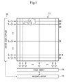
- Fig. 1 is a view for describing a schematic configuration of a touch sensing apparatus according to an embodiment of the present invention.
- the touch sensing apparatus of the present invention includes a touch sensor panel 110 comprised of a plurality of row wirings and a plurality of column wirings, a driving signal supplier 120 which inputs a driving signal to the touch sensor panel 110, a signal sensor 130 which senses a signal outputted from the column wiring, and a frequency hopper 140.
- the driving signal supplier 120, the signal sensor 130 and the frequency hopper 140 may be modules which are controlled by a predetermined signal.
- These parts include routines, subroutines, programs, objects, components, data structures and the like, all of which perform specific operations to be described below or specific algorithms. However, these parts are not limited to this.
- the driving signal supplier 120, the signal sensor 130 and the frequency hopper 140 will be described as separate parts, this is only for convenience of description. At least two of them may be formed in the form of one module.
- the signal sensor 130 and the frequency hopper 140 may be formed in the form of one part capable of performing their respective functions.
- the touch sensor panel 110 is formed in the form of a matrix comprised of row wirings and column wirings.
- the row wiring and the column wiring are separated from each other by a dielectric material.
- a sensor or pixel is located at a point where the row wirings and column wirings cross each other.
- Each row wiring can be driven by a stimulation signal. Therefore, it can be said that the row wiring is a drive line.
- a sensing signal outputted from the column wiring corresponding to a point where the touch has occurred by the driving signal injected into the row wiring becomes different from a signal outputted from another column wiring, so that the location of the touch can be recognized by the signal. Therefore, it can be said that the column wiring is a sensing line.
- a touch sensing panel having an orthogonal array consisting of the row and column will be described as an example, the embodiment of the present invention is not limited to this.
- the embodiment of the present invention can be applied to another touch sensing panel having an array of arbitrary dimension, for example, a diagonal array, a concentric array, a 3-dimensional random array, etc., and an array obtained by the application of them.
- the drive line and the sensing line may be formed of a transparent conductive material (e.g., Indium Tin Oxide (ITO), Antimony Tin Oxide (ATO) or the like).
- a transparent conductive material e.g., Indium Tin Oxide (ITO), Antimony Tin Oxide (ATO) or the like.
- the drive line and the sensing line may be also formed of another transparent material or an opaque conductive material including copper and the like.
- a signal with a specific frequency may be inputted through each drive line.
- the signal may be generated by a driving signal supplier 120.
- the driving signal supplier 120 may input serially the sensing signal to each drive line. For example, on the basis of a clock signal, etc., the driving signal supplier 120 inputs the driving signal to a first drive line D0 during a first interval and inputs the driving signal to a second drive line D1 during a second interval, so that the same driving signal is controlled not to be parallelly inputted to the two or more sensing lines. This is because, when the same driving signal is parallelly inputted to a plurality of the sensing lines, it is impossible to recognize which location of the drive line the touch has occurred on, even though the touch is sensed through a particular sensing line. Therefore, the driving signals must be supplied to the drive lines at mutually different points of time.
- a sensing line passing through the particular location When the touch occurs on a particular location of the touch screen, a sensing line passing through the particular location outputs a signal different from signals outputted from other sensing lines.
- the signal sensor 130 receives the signal outputted from each sensing line and determines which location of the sensing line the touch has occurred on.
- the signal sensor 130 is able to sense a signal having a frequency the same as that of the driving signal supplied by the driving signal supplier 120.
- the signal outputted from the sensing line passing through a point where the touch has occurred may have an amplitude lower than that of a steady-state signal outputted from another sensing line.
- the point where the touch has occurred can be recognized by determining the amplitude difference.
- the signal outputted from each sensing line may be observed parallelly or serially.
- the magnitude of the signal received by the signal sensor 130 may be changed due to the noise.
- noise having the same frequency as that of a current sensing signal, the characteristics of the signal sensed by the signal sensor 130 may be changed.
- the frequency hopper 140 estimate the noise at a current driving signal frequency, finds a frequency having a minimized noise, and thus allows the frequency of the driving signal to be changed into the frequency having a minimized noise.
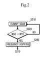
- Fig. 2 is a view for describing a method for minimizing noise in a touch panel according to a first embodiment of the present invention.
- a dummy scan is performed by the signal sensor 130 (S210).
- the dummy scan of the present specification means a process of sensing the signal from the respective sensing lines in a state where the driving signal is not inputted to the drive line. That is, through the dummy scan, the signal from the sensing line may be sensed only one time or at least twice in a state where the driving signal is not applied.
- a driving signal having a specific frequency is inputted to the drive line, and then a signal outputted from the sensing line is sensed.
- the dummy scan may be performed periodically or non-periodically. For example, at every point of time when one cycle ends, during which the touch is sensed by serially inputting the driving signal to the drive lines D0 to Dn respectively, the dummy scan can be performed at least one time in a state where the driving signal is not inputted to all of the drive lines D0 to Dn.
- the frequency hopper 140 compares a threshold NTO with a magnitude NS0 of the signal sensed by the signal sensor 130 through the dummy scan (S220).
- the magnitude NS0 of the signal sensed by the signal sensor 130 may be the average value, the maximum value or the sum of the signals outputted from the sensing lines respectively. However, any variable will be used so long as it can discover even the characteristics of the signal outputted from the sensing line at the presence of the noise. If the magnitude NS0 of the signal sensed by the signal sensor 130 through the dummy scan is less than the threshold NTO, this means that the noise is acceptable in a band of the current driving signal frequency (or the frequency of the signal sensed by the signal sensor 130).
- the driving signal having the frequency same as the current driving signal frequency can be continuously used.
- a single dummy scan can be continuously performed (for example, at every point of time when one cycle ends, during which the touch is sensed by serially inputting the driving signal to all of the drive lines D0 to Dn).
- the frequency hopper 140 changes the frequency of the signal sensed by the signal sensor 130 (S230). This is referred to as "frequency hopping". After the frequency hopping is performed, the single dummy scan may be repetitively performed in the corresponding frequency (S210).
- the frequency hopping S230 may be performed by the following process.
- the dummy scan is performed in a frequency band different from that of the current driving signal (S231).
- the signal sensor 130 senses a signal corresponding to a first frequency band
- the first frequency band is changed into a second frequency band
- the dummy scan is performed.
- a magnitude NS0' of the sensed signal through the dummy scan is compared with the threshold NTO (S232). If the magnitude NS0' of the sensed signal through the dummy scan is less than the threshold NTO, the frequency of the driving signal is changed into the corresponding frequency (S233).
- the frequency band of the signal is changed into a third frequency band, and then the dummy scan is performed again (S231).
- the frequency hopping S230 can be performed in various manners other than the embodiment shown in Fig. 3 .
- the magnitude NS0' of the signal through the dummy scan performed in the frequency changed in step S232 may be compared with the magnitude NS0 of the signal through the dummy scan performed in the frequency before being changed.
- the dummy scan is performed in all the various frequency candidates, and then a frequency having a smallest magnitude may be selected and changed.
- step S230 When the frequency hopping S230 is completed, the corresponding process may be repeated from step S210.
- Fig. 4 is a view for describing a method for minimizing noise in a touch panel according to a second embodiment of the present invention.
- a first dummy scan is performed by the signal sensor 130 (S410).
- the dummy scan means a process of sensing the signal from the respective sensing lines in a state where the driving signal is not inputted to the drive line.
- the first dummy scan in step S410 means that the dummy scan is performed at least one time.
- the magnitude NS0 of the sensed signal is compared with the threshold NTO (S420).
- the magnitude NS0 of the sensed signal may be the average value, the maximum value or the sum of the signals outputted from the sensing lines respectively.
- the driving signal having the frequency same as the current driving signal frequency can be continuously used.
- the first dummy scan can be continuously performed (for example, at every point of time when one cycle ends, during which the touch is sensed by serially inputting the driving signal to all of the drive lines D0 to Dn).
- the magnitude NS0 of the signal sensed by the signal sensor 130 through the dummy scan is greater than the first threshold NTO, this may mean that the noise having the same frequency as that of the current driving signal is not acceptable.
- the frequency hopper 140 performs a second dummy scan (S430).
- the second dummy scan may mean that the dummy scan is performed again at least one time. That is, the signal from the sensing line is sensed at least one time in a state where the driving signal is not applied to the drive line.
- the number of repetition times of the signal sensing may be equal to or not equal to the number of repetition times of the dummy scan in step S410.
- the number of repetition times of the dummy scan in the second dummy scan step S430 may be greater than the number of repetition times of the dummy scan in the first dummy scan step S410.
- a magnitude NS1 of a signal obtained through the second dummy scan is compared with a second threshold NT1 (S440).
- the threshold NT1 may be different from the threshold NTO used in step S420.
- the threshold NT1 used in step S440 may be greater than the threshold NTO used in step S420.
- the magnitude NS1 of the signal obtained through the second dummy scan may be at least one of the average value, the maximum value or the sum of the magnitudes of the signals obtained through the respective dummy scans. However, the magnitude NS1 is not limited to this. If, as a result of the comparison in step S440, the magnitude NS1 of the signal obtained through the second dummy scan is less than the second threshold NT1, the single dummy scan S410 is performed again at the same frequency.
- step S450 and step S460 may be performed. Every time step S410 is performed after step S440, "the number of trials" is increased by 1 (S450). When "the number of trials" is equal to a predetermined repetition threshold value MAX_TRY, step S410 is not performed and a frequency hopping step S470 may be performed. However, the steps S450 and S460 can be omitted.
- step S470 either when the magnitude NS1 of the signal obtained through the second dummy scan is greater than the second threshold NT1 or when the number of repetition times of the steps S410 to S440 is greater than a predetermined number, the frequency hopping is performed (S470).
- the frequency hopping means that the frequency of the signal sensed by the signal sensor 130 is changed.
- the frequency hopping S470 may be performed according to the following process.
- the dummy scan is performed in a frequency band different from the frequency band of the current driving signal (S471).
- the signal sensor 130 senses a signal corresponding to the first frequency band
- the first frequency is changed into the second frequency band, and then the dummy scan is performed at least one time.
- a magnitude NS2 of the signal obtained by performing the dummy scan in the second frequency band is compared with the magnitude NS1 of the signal obtained by performing the dummy scan in the first frequency band (S472). While Fig.
- the magnitude NS1 of the signal obtained by performing the dummy scan in the first frequency band corresponds to the magnitude NS1 of the signal obtained through the second dummy scan in step S430 (see Fig. 4 )
- the magnitude NS1 of the signal obtained by performing the dummy scan in the first frequency band may be replaced by the magnitude NS0 of the signal obtained through the first dummy scan in step S410.
- step S472 If, as a result of the comparison in step S472, the magnitude NS2 of the signal obtained by performing the dummy scan in the second frequency band is less than the magnitude NS1 of the signal obtained by performing the dummy scan in the first frequency band, the frequency of the driving signal is changed into the corresponding frequency (S473). However, if not, the frequency of the driving signal is changed into the third frequency, and then the dummy scan is performed again (S471).
- the frequency hopping S470 may be performed according to the following process.
- the dummy scan is performed in a frequency band different from the frequency band of the current driving signal (S474).
- the signal sensor 130 senses a signal corresponding to the first frequency band
- the first frequency is changed into the second frequency band, and then the dummy scan is performed at least one time.
- the magnitude NS2 of the signal obtained by performing the single dummy scan in the second frequency band is compared with the threshold NTO (S475).
- this threshold NT0 may be equal to the threshold NTO which is a target to be compared with the magnitude NS0 of the signal obtained through the first dummy scan in step S420 (see Fig.
- this threshold NTO may be equal to the threshold NT1 which is a target to be compared with the magnitude NS1 of the signal obtained through the second dummy scan in step S440 or may be another third threshold.
- the magnitude NS2 of the signal obtained by performing the dummy scan in the second frequency band is less than the threshold NTO, the frequency of the driving signal is changed into the corresponding frequency (S476). However, if not, the frequency of the driving signal is changed into the third frequency, and then the dummy scan is performed again (S474).
- the frequency hopping S470 can be performed in various manners other than the embodiments shown in Figs. 5 and 6 .
- a modified example of the above-described method shown in Fig. 5 will be provided.
- the magnitude NS2 of the signal obtained through the dummy scan in the second frequency band may be compared with the threshold NT1 used in step S440 (see Fig. 4 ).
- the dummy scan is performed in all the various frequency candidates, and then a frequency having a smallest magnitude may be selected and changed.
- the corresponding process may be repeated from step S410 or step 430. That is, after the frequency hopping is completed, it is possible that the first dummy scan is performed in the changed frequency band (S410) and then the noise is estimated, or the second dummy scan is performed with the omission of the first dummy scan (S430) and then the noise is estimated.
- any reference in this specification to "one embodiment,” “an embodiment,” “example embodiment,” etc. means that a particular feature, structure, or characteristic described in connection with the embodiment is included in at least one embodiment of the invention.
- the appearances of such phrases in various places in the specification are not necessarily all referring to the same embodiment.
Landscapes
- Engineering & Computer Science (AREA)
- General Engineering & Computer Science (AREA)
- Theoretical Computer Science (AREA)
- Physics & Mathematics (AREA)
- General Physics & Mathematics (AREA)
- Human Computer Interaction (AREA)
- Nonlinear Science (AREA)
- Mathematical Physics (AREA)
- Chemical & Material Sciences (AREA)
- Crystallography & Structural Chemistry (AREA)
- Optics & Photonics (AREA)
- Position Input By Displaying (AREA)
Applications Claiming Priority (1)
| Application Number | Priority Date | Filing Date | Title |
|---|---|---|---|
| KR1020120031638A KR101378511B1 (ko) | 2012-03-28 | 2012-03-28 | 터치 패널에서 노이즈를 최소화하기 위한 방법, 터치 감지 장치 및 컴퓨터 판독 가능한 기록 매체 |
Publications (3)
| Publication Number | Publication Date |
|---|---|
| EP2645210A2 true EP2645210A2 (fr) | 2013-10-02 |
| EP2645210A3 EP2645210A3 (fr) | 2016-06-01 |
| EP2645210B1 EP2645210B1 (fr) | 2018-12-05 |
Family
ID=47900784
Family Applications (1)
| Application Number | Title | Priority Date | Filing Date |
|---|---|---|---|
| EP13159102.6A Active EP2645210B1 (fr) | 2012-03-28 | 2013-03-14 | Procédé et appareil tactile pour minimiser le bruit sur l'écran tactile |
Country Status (4)
| Country | Link |
|---|---|
| US (1) | US9223437B2 (fr) |
| EP (1) | EP2645210B1 (fr) |
| JP (1) | JP2013206463A (fr) |
| KR (1) | KR101378511B1 (fr) |
Families Citing this family (16)
| Publication number | Priority date | Publication date | Assignee | Title |
|---|---|---|---|---|
| CN102830837B (zh) * | 2012-07-19 | 2016-01-27 | 深圳市汇顶科技股份有限公司 | 一种用于触摸检测的噪声抑制方法、系统及触摸终端 |
| KR102132865B1 (ko) * | 2013-12-23 | 2020-07-10 | 엘지디스플레이 주식회사 | 표시장치 및 그 구동방법 |
| KR102295877B1 (ko) | 2014-12-03 | 2021-08-31 | 엘지디스플레이 주식회사 | 액정표시패널 및 이를 이용한 액정표시장치 |
| KR102276911B1 (ko) * | 2015-01-14 | 2021-07-13 | 삼성전자주식회사 | 터치 컨트롤러, 터치 센싱 장치 및 터치 센싱 방법 |
| EP3159777B1 (fr) | 2015-10-20 | 2024-05-29 | LG Display Co., Ltd. | Procédé et circuit pour l'entraînement de capteurs tactiles et dispositif d'affichage utilisant ceux-ci |
| KR102489286B1 (ko) * | 2015-10-20 | 2023-01-18 | 엘지디스플레이 주식회사 | 표시패널의 구동 회로 및 이를 포함한 표시장치 |
| WO2020050634A1 (fr) * | 2018-09-06 | 2020-03-12 | 주식회사 하이딥 | Procédé d'attaque de panneau tactile et dispositif d'entrée tactile |
| KR102159067B1 (ko) * | 2018-09-06 | 2020-09-23 | 주식회사 하이딥 | 터치센서패널 구동방법 및 터치입력장치 |
| WO2020049781A1 (fr) * | 2018-09-07 | 2020-03-12 | アルプスアルパイン株式会社 | Dispositif capteur et procédé de commande et programme associés |
| KR102804945B1 (ko) * | 2019-12-24 | 2025-05-09 | 주식회사 엘엑스세미콘 | 노이즈를 회피하는 터치센싱장치 및 이를 포함하는 표시장치 |
| KR102349856B1 (ko) * | 2020-04-28 | 2022-01-11 | 주식회사 하이딥 | 터치 입력 장치 |
| US11550434B2 (en) * | 2020-10-19 | 2023-01-10 | Synaptics Incorporated | Short-term noise suppression |
| CN113760129A (zh) * | 2021-09-06 | 2021-12-07 | 合肥松豪电子科技有限公司 | 一种检测tp芯片噪声的方法 |
| WO2024112168A1 (fr) * | 2022-11-25 | 2024-05-30 | 주식회사 엘엑스세미콘 | Dispositif de commande tactile et dispositif d'affichage |
| KR20250093671A (ko) | 2023-12-15 | 2025-06-25 | 삼성디스플레이 주식회사 | 입력 센싱부 및 그것의 노이즈 감소 방법 |
| US12443311B1 (en) * | 2024-07-18 | 2025-10-14 | Stmicroelectronics International N.V. | Touch screen display and method of operating the same |
Family Cites Families (26)
| Publication number | Priority date | Publication date | Assignee | Title |
|---|---|---|---|---|
| US5565658A (en) | 1992-07-13 | 1996-10-15 | Cirque Corporation | Capacitance-based proximity with interference rejection apparatus and methods |
| JP3270544B2 (ja) * | 1992-11-19 | 2002-04-02 | キヤノン株式会社 | 座標入力装置 |
| JP3249862B2 (ja) * | 1993-09-27 | 2002-01-21 | 株式会社ワコム | 位置検出装置 |
| JP3436637B2 (ja) * | 1996-06-04 | 2003-08-11 | アルプス電気株式会社 | 座標入力装置 |
| KR100659048B1 (ko) * | 2000-09-06 | 2006-12-18 | 삼성에스디아이 주식회사 | 외부 노이즈를 차단할 수 있는 더미전극을 구비한 터치패널 |
| US7031886B1 (en) * | 2004-12-14 | 2006-04-18 | Synaptics Incorporated | Methods and systems for detecting noise in a position sensor using minor shifts in sensing frequency |
| US8279180B2 (en) * | 2006-05-02 | 2012-10-02 | Apple Inc. | Multipoint touch surface controller |
| KR101297387B1 (ko) * | 2006-11-09 | 2013-08-19 | 삼성디스플레이 주식회사 | 터치 패널 일체형 액정 표시 장치 |
| US7643011B2 (en) * | 2007-01-03 | 2010-01-05 | Apple Inc. | Noise detection in multi-touch sensors |
| US7986193B2 (en) * | 2007-01-03 | 2011-07-26 | Apple Inc. | Noise reduction within an electronic device using automatic frequency modulation |
| US7876311B2 (en) * | 2007-06-13 | 2011-01-25 | Apple Inc. | Detection of low noise frequencies for multiple frequency sensor panel stimulation |
| US8493331B2 (en) * | 2007-06-13 | 2013-07-23 | Apple Inc. | Touch detection using multiple simultaneous frequencies |
| US8054090B2 (en) * | 2008-10-22 | 2011-11-08 | Atmel Corporation | Noise handling in capacitive touch sensors |
| US9036650B2 (en) * | 2009-09-11 | 2015-05-19 | Apple Inc. | Automatic low noise frequency selection |
| TWI421820B (zh) * | 2009-10-16 | 2014-01-01 | Ind Tech Res Inst | 顯示裝置、電子系統以及控制方法 |
| US8836666B2 (en) * | 2010-10-31 | 2014-09-16 | Pixart Imaging Inc. | Method and device for reducing noise interference in a capacitive touchscreen system |
| US8860432B2 (en) * | 2011-02-25 | 2014-10-14 | Maxim Integrated Products, Inc. | Background noise measurement and frequency selection in touch panel sensor systems |
| US9092098B2 (en) * | 2011-04-19 | 2015-07-28 | Cypress Semiconductor Corporation | Method and apparatus to improve noise immunity of a touch sense array |
| US20130069894A1 (en) * | 2011-09-16 | 2013-03-21 | Htc Corporation | Electronic device and method for driving a touch sensor thereof |
| KR101124713B1 (ko) | 2011-09-28 | 2012-03-12 | (주)이미지스테크놀로지 | 정전용량 방식 터치 패널에서의 스캔 방향 스위칭에 의한 노이즈 제거 방법 |
| KR101328228B1 (ko) * | 2011-11-21 | 2013-11-14 | 삼성전기주식회사 | 접촉 감지 장치 및 접촉 감지 방법 |
| US9372581B2 (en) * | 2012-01-09 | 2016-06-21 | Broadcom Corporation | Interference estimation and adaptive reconfiguration of a capacitive touch controller |
| US8970547B2 (en) * | 2012-02-01 | 2015-03-03 | Synaptics Incorporated | Noise-adapting touch sensing window |
| US8294687B1 (en) * | 2012-02-23 | 2012-10-23 | Cypress Semiconductor Corporation | False touch filtering for capacitance sensing systems |
| US9164635B2 (en) * | 2012-05-07 | 2015-10-20 | Melfas Inc. | Touch sensor chip, touch sensing apparatus including the same, and method of controlling noise of touch panel |
| US8874396B1 (en) * | 2013-06-28 | 2014-10-28 | Cypress Semiconductor Corporation | Injected touch noise analysis |
-
2012
- 2012-03-28 KR KR1020120031638A patent/KR101378511B1/ko active Active
-
2013
- 2013-03-12 US US13/797,202 patent/US9223437B2/en active Active
- 2013-03-14 EP EP13159102.6A patent/EP2645210B1/fr active Active
- 2013-03-18 JP JP2013054593A patent/JP2013206463A/ja active Pending
Also Published As
| Publication number | Publication date |
|---|---|
| EP2645210A3 (fr) | 2016-06-01 |
| KR101378511B1 (ko) | 2014-03-27 |
| EP2645210B1 (fr) | 2018-12-05 |
| KR20130109691A (ko) | 2013-10-08 |
| JP2013206463A (ja) | 2013-10-07 |
| US9223437B2 (en) | 2015-12-29 |
| US20130257765A1 (en) | 2013-10-03 |
Similar Documents
| Publication | Publication Date | Title |
|---|---|---|
| EP2645210A2 (fr) | Procédé, appareil tactile et support d'enregistrement lisible par ordinateur pour minimiser le bruit sur l'écran tactile | |
| KR102692409B1 (ko) | 구동 방법, 터치 센싱 회로, 표시패널 및 터치 표시 장치 | |
| CN104252070B (zh) | 显示设备及其驱动方法 | |
| KR101338285B1 (ko) | 터치 패널에서 터치를 감지하기 위한 방법, 장치 및 컴퓨터 판독 가능 기록 매체 | |
| CN112925448B (zh) | 一种触控显示面板及其检测方法、触控显示装置 | |
| US9886115B2 (en) | Touch display substrate | |
| US9063606B2 (en) | Control device for a touch panel | |
| US20140198053A1 (en) | Method, device and computer-readable recording medium for sensing touch on touch panel | |
| US20150220170A1 (en) | Touch-sensing apparatus and method | |
| WO2020107435A1 (fr) | Circuit de balayage, circuit de dispositif d'attaque, panneau d'affichage tactile, circuit de commutation de récepteur et procédé d'attaque | |
| US8604798B2 (en) | Short-circuit detection for touch panels | |
| US20120098786A1 (en) | Control Device for a Touch Panel | |
| EP3260962A1 (fr) | Écran tactile en cellule et dispositif d'affichage | |
| US10423252B2 (en) | Array substrate, touch display panel, and touch display device | |
| US8743085B2 (en) | Touch input device for switching driving signals | |
| US20210397285A1 (en) | Method and apparatus for determining a touch point | |
| US9582099B2 (en) | Serrated input sensing intervals | |
| KR20140105299A (ko) | 터치패널 입력장치 및 그의 터치패널 입력검출방법 | |
| US20160202828A1 (en) | Touch panel and method for detecting the same | |
| CN111045549A (zh) | 显示面板及其驱动方法和显示装置 | |
| KR101748568B1 (ko) | 단층 감지 패턴을 이용한 터치 패널 및 상기 터치 패널을 포함하는 터치 감지 장치 | |
| US10545606B2 (en) | Scanning circuit for touch screen, touch screen and touch control method | |
| KR102020280B1 (ko) | 터치 패널 장치와 이의 구동 방법 | |
| US20210223932A1 (en) | Method for controlling a flexible capacitive touch display panel and touch display apparatus | |
| US10055045B2 (en) | Current feedback digital charge accumulator |
Legal Events
| Date | Code | Title | Description |
|---|---|---|---|
| PUAI | Public reference made under article 153(3) epc to a published international application that has entered the european phase |
Free format text: ORIGINAL CODE: 0009012 |
|
| 17P | Request for examination filed |
Effective date: 20130408 |
|
| AK | Designated contracting states |
Kind code of ref document: A2 Designated state(s): AL AT BE BG CH CY CZ DE DK EE ES FI FR GB GR HR HU IE IS IT LI LT LU LV MC MK MT NL NO PL PT RO RS SE SI SK SM TR |
|
| AX | Request for extension of the european patent |
Extension state: BA ME |
|
| PUAL | Search report despatched |
Free format text: ORIGINAL CODE: 0009013 |
|
| AK | Designated contracting states |
Kind code of ref document: A3 Designated state(s): AL AT BE BG CH CY CZ DE DK EE ES FI FR GB GR HR HU IE IS IT LI LT LU LV MC MK MT NL NO PL PT RO RS SE SI SK SM TR |
|
| AX | Request for extension of the european patent |
Extension state: BA ME |
|
| RIC1 | Information provided on ipc code assigned before grant |
Ipc: H04B 15/04 20060101ALI20160428BHEP Ipc: G06F 3/041 20060101AFI20160428BHEP Ipc: G06F 3/044 20060101ALI20160428BHEP |
|
| RBV | Designated contracting states (corrected) |
Designated state(s): AL AT BE BG CH CY CZ DE DK EE ES FI FR GB GR HR HU IE IS IT LI LT LU LV MC MK MT NL NO PL PT RO RS SE SI SK SM TR |
|
| STAA | Information on the status of an ep patent application or granted ep patent |
Free format text: STATUS: EXAMINATION IS IN PROGRESS |
|
| 17Q | First examination report despatched |
Effective date: 20170817 |
|
| GRAP | Despatch of communication of intention to grant a patent |
Free format text: ORIGINAL CODE: EPIDOSNIGR1 |
|
| STAA | Information on the status of an ep patent application or granted ep patent |
Free format text: STATUS: GRANT OF PATENT IS INTENDED |
|
| RIC1 | Information provided on ipc code assigned before grant |
Ipc: H04M 1/02 20060101ALI20180706BHEP Ipc: G06F 3/041 20060101AFI20180706BHEP |
|
| INTG | Intention to grant announced |
Effective date: 20180725 |
|
| RIN1 | Information on inventor provided before grant (corrected) |
Inventor name: LEE, HWANHEE Inventor name: YOON, SANGSIC |
|
| GRAS | Grant fee paid |
Free format text: ORIGINAL CODE: EPIDOSNIGR3 |
|
| GRAJ | Information related to disapproval of communication of intention to grant by the applicant or resumption of examination proceedings by the epo deleted |
Free format text: ORIGINAL CODE: EPIDOSDIGR1 |
|
| GRAL | Information related to payment of fee for publishing/printing deleted |
Free format text: ORIGINAL CODE: EPIDOSDIGR3 |
|
| STAA | Information on the status of an ep patent application or granted ep patent |
Free format text: STATUS: EXAMINATION IS IN PROGRESS |
|
| GRAJ | Information related to disapproval of communication of intention to grant by the applicant or resumption of examination proceedings by the epo deleted |
Free format text: ORIGINAL CODE: EPIDOSDIGR1 |
|
| GRAP | Despatch of communication of intention to grant a patent |
Free format text: ORIGINAL CODE: EPIDOSNIGR1 |
|
| GRAP | Despatch of communication of intention to grant a patent |
Free format text: ORIGINAL CODE: EPIDOSNIGR1 |
|
| STAA | Information on the status of an ep patent application or granted ep patent |
Free format text: STATUS: GRANT OF PATENT IS INTENDED |
|
| INTC | Intention to grant announced (deleted) | ||
| GRAA | (expected) grant |
Free format text: ORIGINAL CODE: 0009210 |
|
| INTG | Intention to grant announced |
Effective date: 20181012 |
|
| GRAA | (expected) grant |
Free format text: ORIGINAL CODE: 0009210 |
|
| STAA | Information on the status of an ep patent application or granted ep patent |
Free format text: STATUS: THE PATENT HAS BEEN GRANTED |
|
| AK | Designated contracting states |
Kind code of ref document: B1 Designated state(s): AL AT BE BG CH CY CZ DE DK EE ES FI FR GB GR HR HU IE IS IT LI LT LU LV MC MK MT NL NO PL PT RO RS SE SI SK SM TR |
|
| REG | Reference to a national code |
Ref country code: GB Ref legal event code: FG4D |
|
| REG | Reference to a national code |
Ref country code: CH Ref legal event code: EP |
|
| REG | Reference to a national code |
Ref country code: AT Ref legal event code: REF Ref document number: 1073875 Country of ref document: AT Kind code of ref document: T Effective date: 20181215 |
|
| REG | Reference to a national code |
Ref country code: DE Ref legal event code: R096 Ref document number: 602013047675 Country of ref document: DE |
|
| REG | Reference to a national code |
Ref country code: IE Ref legal event code: FG4D |
|
| REG | Reference to a national code |
Ref country code: NL Ref legal event code: MP Effective date: 20181205 |
|
| REG | Reference to a national code |
Ref country code: AT Ref legal event code: MK05 Ref document number: 1073875 Country of ref document: AT Kind code of ref document: T Effective date: 20181205 |
|
| REG | Reference to a national code |
Ref country code: LT Ref legal event code: MG4D |
|
| PG25 | Lapsed in a contracting state [announced via postgrant information from national office to epo] |
Ref country code: BG Free format text: LAPSE BECAUSE OF FAILURE TO SUBMIT A TRANSLATION OF THE DESCRIPTION OR TO PAY THE FEE WITHIN THE PRESCRIBED TIME-LIMIT Effective date: 20190305 Ref country code: NO Free format text: LAPSE BECAUSE OF FAILURE TO SUBMIT A TRANSLATION OF THE DESCRIPTION OR TO PAY THE FEE WITHIN THE PRESCRIBED TIME-LIMIT Effective date: 20190305 Ref country code: HR Free format text: LAPSE BECAUSE OF FAILURE TO SUBMIT A TRANSLATION OF THE DESCRIPTION OR TO PAY THE FEE WITHIN THE PRESCRIBED TIME-LIMIT Effective date: 20181205 Ref country code: LT Free format text: LAPSE BECAUSE OF FAILURE TO SUBMIT A TRANSLATION OF THE DESCRIPTION OR TO PAY THE FEE WITHIN THE PRESCRIBED TIME-LIMIT Effective date: 20181205 Ref country code: ES Free format text: LAPSE BECAUSE OF FAILURE TO SUBMIT A TRANSLATION OF THE DESCRIPTION OR TO PAY THE FEE WITHIN THE PRESCRIBED TIME-LIMIT Effective date: 20181205 Ref country code: LV Free format text: LAPSE BECAUSE OF FAILURE TO SUBMIT A TRANSLATION OF THE DESCRIPTION OR TO PAY THE FEE WITHIN THE PRESCRIBED TIME-LIMIT Effective date: 20181205 Ref country code: AT Free format text: LAPSE BECAUSE OF FAILURE TO SUBMIT A TRANSLATION OF THE DESCRIPTION OR TO PAY THE FEE WITHIN THE PRESCRIBED TIME-LIMIT Effective date: 20181205 Ref country code: FI Free format text: LAPSE BECAUSE OF FAILURE TO SUBMIT A TRANSLATION OF THE DESCRIPTION OR TO PAY THE FEE WITHIN THE PRESCRIBED TIME-LIMIT Effective date: 20181205 |
|
| PG25 | Lapsed in a contracting state [announced via postgrant information from national office to epo] |
Ref country code: AL Free format text: LAPSE BECAUSE OF FAILURE TO SUBMIT A TRANSLATION OF THE DESCRIPTION OR TO PAY THE FEE WITHIN THE PRESCRIBED TIME-LIMIT Effective date: 20181205 Ref country code: RS Free format text: LAPSE BECAUSE OF FAILURE TO SUBMIT A TRANSLATION OF THE DESCRIPTION OR TO PAY THE FEE WITHIN THE PRESCRIBED TIME-LIMIT Effective date: 20181205 Ref country code: SE Free format text: LAPSE BECAUSE OF FAILURE TO SUBMIT A TRANSLATION OF THE DESCRIPTION OR TO PAY THE FEE WITHIN THE PRESCRIBED TIME-LIMIT Effective date: 20181205 Ref country code: GR Free format text: LAPSE BECAUSE OF FAILURE TO SUBMIT A TRANSLATION OF THE DESCRIPTION OR TO PAY THE FEE WITHIN THE PRESCRIBED TIME-LIMIT Effective date: 20190306 |
|
| PG25 | Lapsed in a contracting state [announced via postgrant information from national office to epo] |
Ref country code: NL Free format text: LAPSE BECAUSE OF FAILURE TO SUBMIT A TRANSLATION OF THE DESCRIPTION OR TO PAY THE FEE WITHIN THE PRESCRIBED TIME-LIMIT Effective date: 20181205 |
|
| PG25 | Lapsed in a contracting state [announced via postgrant information from national office to epo] |
Ref country code: IT Free format text: LAPSE BECAUSE OF FAILURE TO SUBMIT A TRANSLATION OF THE DESCRIPTION OR TO PAY THE FEE WITHIN THE PRESCRIBED TIME-LIMIT Effective date: 20181205 Ref country code: PT Free format text: LAPSE BECAUSE OF FAILURE TO SUBMIT A TRANSLATION OF THE DESCRIPTION OR TO PAY THE FEE WITHIN THE PRESCRIBED TIME-LIMIT Effective date: 20190405 Ref country code: CZ Free format text: LAPSE BECAUSE OF FAILURE TO SUBMIT A TRANSLATION OF THE DESCRIPTION OR TO PAY THE FEE WITHIN THE PRESCRIBED TIME-LIMIT Effective date: 20181205 Ref country code: PL Free format text: LAPSE BECAUSE OF FAILURE TO SUBMIT A TRANSLATION OF THE DESCRIPTION OR TO PAY THE FEE WITHIN THE PRESCRIBED TIME-LIMIT Effective date: 20181205 |
|
| PG25 | Lapsed in a contracting state [announced via postgrant information from national office to epo] |
Ref country code: IS Free format text: LAPSE BECAUSE OF FAILURE TO SUBMIT A TRANSLATION OF THE DESCRIPTION OR TO PAY THE FEE WITHIN THE PRESCRIBED TIME-LIMIT Effective date: 20190405 Ref country code: RO Free format text: LAPSE BECAUSE OF FAILURE TO SUBMIT A TRANSLATION OF THE DESCRIPTION OR TO PAY THE FEE WITHIN THE PRESCRIBED TIME-LIMIT Effective date: 20181205 Ref country code: SK Free format text: LAPSE BECAUSE OF FAILURE TO SUBMIT A TRANSLATION OF THE DESCRIPTION OR TO PAY THE FEE WITHIN THE PRESCRIBED TIME-LIMIT Effective date: 20181205 Ref country code: EE Free format text: LAPSE BECAUSE OF FAILURE TO SUBMIT A TRANSLATION OF THE DESCRIPTION OR TO PAY THE FEE WITHIN THE PRESCRIBED TIME-LIMIT Effective date: 20181205 Ref country code: SM Free format text: LAPSE BECAUSE OF FAILURE TO SUBMIT A TRANSLATION OF THE DESCRIPTION OR TO PAY THE FEE WITHIN THE PRESCRIBED TIME-LIMIT Effective date: 20181205 |
|
| REG | Reference to a national code |
Ref country code: DE Ref legal event code: R097 Ref document number: 602013047675 Country of ref document: DE |
|
| REG | Reference to a national code |
Ref country code: DE Ref legal event code: R119 Ref document number: 602013047675 Country of ref document: DE Ref country code: DE Ref legal event code: R409 Ref document number: 602013047675 Country of ref document: DE |
|
| PLBE | No opposition filed within time limit |
Free format text: ORIGINAL CODE: 0009261 |
|
| STAA | Information on the status of an ep patent application or granted ep patent |
Free format text: STATUS: NO OPPOSITION FILED WITHIN TIME LIMIT |
|
| PG25 | Lapsed in a contracting state [announced via postgrant information from national office to epo] |
Ref country code: DK Free format text: LAPSE BECAUSE OF FAILURE TO SUBMIT A TRANSLATION OF THE DESCRIPTION OR TO PAY THE FEE WITHIN THE PRESCRIBED TIME-LIMIT Effective date: 20181205 Ref country code: SI Free format text: LAPSE BECAUSE OF FAILURE TO SUBMIT A TRANSLATION OF THE DESCRIPTION OR TO PAY THE FEE WITHIN THE PRESCRIBED TIME-LIMIT Effective date: 20181205 Ref country code: MC Free format text: LAPSE BECAUSE OF FAILURE TO SUBMIT A TRANSLATION OF THE DESCRIPTION OR TO PAY THE FEE WITHIN THE PRESCRIBED TIME-LIMIT Effective date: 20181205 |
|
| REG | Reference to a national code |
Ref country code: CH Ref legal event code: PL |
|
| 26N | No opposition filed |
Effective date: 20190906 |
|
| PG25 | Lapsed in a contracting state [announced via postgrant information from national office to epo] |
Ref country code: LU Free format text: LAPSE BECAUSE OF NON-PAYMENT OF DUE FEES Effective date: 20190314 |
|
| REG | Reference to a national code |
Ref country code: BE Ref legal event code: MM Effective date: 20190331 |
|
| PG25 | Lapsed in a contracting state [announced via postgrant information from national office to epo] |
Ref country code: IE Free format text: LAPSE BECAUSE OF NON-PAYMENT OF DUE FEES Effective date: 20190314 Ref country code: DE Free format text: LAPSE BECAUSE OF NON-PAYMENT OF DUE FEES Effective date: 20191001 Ref country code: LI Free format text: LAPSE BECAUSE OF NON-PAYMENT OF DUE FEES Effective date: 20190331 Ref country code: CH Free format text: LAPSE BECAUSE OF NON-PAYMENT OF DUE FEES Effective date: 20190331 |
|
| PG25 | Lapsed in a contracting state [announced via postgrant information from national office to epo] |
Ref country code: BE Free format text: LAPSE BECAUSE OF NON-PAYMENT OF DUE FEES Effective date: 20190331 |
|
| PG25 | Lapsed in a contracting state [announced via postgrant information from national office to epo] |
Ref country code: TR Free format text: LAPSE BECAUSE OF FAILURE TO SUBMIT A TRANSLATION OF THE DESCRIPTION OR TO PAY THE FEE WITHIN THE PRESCRIBED TIME-LIMIT Effective date: 20181205 |
|
| PG25 | Lapsed in a contracting state [announced via postgrant information from national office to epo] |
Ref country code: MT Free format text: LAPSE BECAUSE OF NON-PAYMENT OF DUE FEES Effective date: 20190314 |
|
| PG25 | Lapsed in a contracting state [announced via postgrant information from national office to epo] |
Ref country code: CY Free format text: LAPSE BECAUSE OF FAILURE TO SUBMIT A TRANSLATION OF THE DESCRIPTION OR TO PAY THE FEE WITHIN THE PRESCRIBED TIME-LIMIT Effective date: 20181205 |
|
| PG25 | Lapsed in a contracting state [announced via postgrant information from national office to epo] |
Ref country code: HU Free format text: LAPSE BECAUSE OF FAILURE TO SUBMIT A TRANSLATION OF THE DESCRIPTION OR TO PAY THE FEE WITHIN THE PRESCRIBED TIME-LIMIT; INVALID AB INITIO Effective date: 20130314 |
|
| PG25 | Lapsed in a contracting state [announced via postgrant information from national office to epo] |
Ref country code: MK Free format text: LAPSE BECAUSE OF FAILURE TO SUBMIT A TRANSLATION OF THE DESCRIPTION OR TO PAY THE FEE WITHIN THE PRESCRIBED TIME-LIMIT Effective date: 20181205 |
|
| PGFP | Annual fee paid to national office [announced via postgrant information from national office to epo] |
Ref country code: DE Payment date: 20250519 Year of fee payment: 13 |
|
| PGFP | Annual fee paid to national office [announced via postgrant information from national office to epo] |
Ref country code: GB Payment date: 20260330 Year of fee payment: 14 |
|
| PGFP | Annual fee paid to national office [announced via postgrant information from national office to epo] |
Ref country code: FR Payment date: 20260330 Year of fee payment: 14 |