EP2645565B1 - Topologie d'amplificateur entièrement différentiel pour entraîner des haut-parleurs dynamiques en mode de classe AB - Google Patents
Topologie d'amplificateur entièrement différentiel pour entraîner des haut-parleurs dynamiques en mode de classe AB Download PDFInfo
- Publication number
- EP2645565B1 EP2645565B1 EP12368006.8A EP12368006A EP2645565B1 EP 2645565 B1 EP2645565 B1 EP 2645565B1 EP 12368006 A EP12368006 A EP 12368006A EP 2645565 B1 EP2645565 B1 EP 2645565B1
- Authority
- EP
- European Patent Office
- Prior art keywords
- transistors
- pair
- transistor
- branch
- differential
- Prior art date
- Legal status (The legal status is an assumption and is not a legal conclusion. Google has not performed a legal analysis and makes no representation as to the accuracy of the status listed.)
- Active
Links
Images


Classifications
-
- H—ELECTRICITY
- H03—ELECTRONIC CIRCUITRY
- H03F—AMPLIFIERS
- H03F3/00—Amplifiers with only discharge tubes or only semiconductor devices as amplifying elements
- H03F3/45—Differential amplifiers
- H03F3/45071—Differential amplifiers with semiconductor devices only
- H03F3/45076—Differential amplifiers with semiconductor devices only characterised by the way of implementation of the active amplifying circuit in the differential amplifier
- H03F3/45179—Differential amplifiers with semiconductor devices only characterised by the way of implementation of the active amplifying circuit in the differential amplifier using MOSFET transistors as the active amplifying circuit
- H03F3/45183—Long tailed pairs
-
- H—ELECTRICITY
- H03—ELECTRONIC CIRCUITRY
- H03F—AMPLIFIERS
- H03F1/00—Details of amplifiers with only discharge tubes, only semiconductor devices or only unspecified devices as amplifying elements
- H03F1/02—Modifications of amplifiers to raise the efficiency, e.g. gliding Class A stages, use of an auxiliary oscillation
- H03F1/0205—Modifications of amplifiers to raise the efficiency, e.g. gliding Class A stages, use of an auxiliary oscillation in transistor amplifiers
- H03F1/0211—Modifications of amplifiers to raise the efficiency, e.g. gliding Class A stages, use of an auxiliary oscillation in transistor amplifiers with control of the supply voltage or current
-
- H—ELECTRICITY
- H03—ELECTRONIC CIRCUITRY
- H03F—AMPLIFIERS
- H03F1/00—Details of amplifiers with only discharge tubes, only semiconductor devices or only unspecified devices as amplifying elements
- H03F1/02—Modifications of amplifiers to raise the efficiency, e.g. gliding Class A stages, use of an auxiliary oscillation
- H03F1/0205—Modifications of amplifiers to raise the efficiency, e.g. gliding Class A stages, use of an auxiliary oscillation in transistor amplifiers
- H03F1/0261—Modifications of amplifiers to raise the efficiency, e.g. gliding Class A stages, use of an auxiliary oscillation in transistor amplifiers with control of the polarisation voltage or current, e.g. gliding Class A
- H03F1/0272—Modifications of amplifiers to raise the efficiency, e.g. gliding Class A stages, use of an auxiliary oscillation in transistor amplifiers with control of the polarisation voltage or current, e.g. gliding Class A by using a signal derived from the output signal
-
- H—ELECTRICITY
- H03—ELECTRONIC CIRCUITRY
- H03F—AMPLIFIERS
- H03F3/00—Amplifiers with only discharge tubes or only semiconductor devices as amplifying elements
- H03F3/30—Single-ended push-pull [SEPP] amplifiers; Phase-splitters therefor
- H03F3/3001—Single-ended push-pull [SEPP] amplifiers; Phase-splitters therefor with field-effect transistors
- H03F3/3022—CMOS common source output SEPP amplifiers
- H03F3/3028—CMOS common source output SEPP amplifiers with symmetrical driving of the end stage
-
- H—ELECTRICITY
- H03—ELECTRONIC CIRCUITRY
- H03F—AMPLIFIERS
- H03F3/00—Amplifiers with only discharge tubes or only semiconductor devices as amplifying elements
- H03F3/45—Differential amplifiers
- H03F3/45071—Differential amplifiers with semiconductor devices only
- H03F3/45479—Differential amplifiers with semiconductor devices only characterised by the way of common mode signal rejection
- H03F3/45632—Differential amplifiers with semiconductor devices only characterised by the way of common mode signal rejection in differential amplifiers with FET transistors as the active amplifying circuit
- H03F3/45636—Differential amplifiers with semiconductor devices only characterised by the way of common mode signal rejection in differential amplifiers with FET transistors as the active amplifying circuit by using feedback means
- H03F3/45641—Measuring at the loading circuit of the differential amplifier
- H03F3/4565—Controlling the common source circuit of the differential amplifier
-
- H—ELECTRICITY
- H03—ELECTRONIC CIRCUITRY
- H03F—AMPLIFIERS
- H03F3/00—Amplifiers with only discharge tubes or only semiconductor devices as amplifying elements
- H03F3/45—Differential amplifiers
- H03F3/45071—Differential amplifiers with semiconductor devices only
- H03F3/45479—Differential amplifiers with semiconductor devices only characterised by the way of common mode signal rejection
- H03F3/45632—Differential amplifiers with semiconductor devices only characterised by the way of common mode signal rejection in differential amplifiers with FET transistors as the active amplifying circuit
- H03F3/45636—Differential amplifiers with semiconductor devices only characterised by the way of common mode signal rejection in differential amplifiers with FET transistors as the active amplifying circuit by using feedback means
- H03F3/45641—Measuring at the loading circuit of the differential amplifier
- H03F3/45659—Controlling the loading circuit of the differential amplifier
-
- H—ELECTRICITY
- H03—ELECTRONIC CIRCUITRY
- H03F—AMPLIFIERS
- H03F2200/00—Indexing scheme relating to amplifiers
- H03F2200/03—Indexing scheme relating to amplifiers the amplifier being designed for audio applications
-
- H—ELECTRICITY
- H03—ELECTRONIC CIRCUITRY
- H03F—AMPLIFIERS
- H03F2200/00—Indexing scheme relating to amplifiers
- H03F2200/513—Indexing scheme relating to amplifiers the amplifier being made for low supply voltages
-
- H—ELECTRICITY
- H03—ELECTRONIC CIRCUITRY
- H03F—AMPLIFIERS
- H03F2200/00—Indexing scheme relating to amplifiers
- H03F2200/516—Some amplifier stages of an amplifier use supply voltages of different value
-
- H—ELECTRICITY
- H03—ELECTRONIC CIRCUITRY
- H03F—AMPLIFIERS
- H03F2203/00—Indexing scheme relating to amplifiers with only discharge tubes or only semiconductor devices as amplifying elements covered by H03F3/00
- H03F2203/45—Indexing scheme relating to differential amplifiers
- H03F2203/45082—Indexing scheme relating to differential amplifiers the common mode signal being taken or deducted from the one or more outputs of the differential amplifier
-
- H—ELECTRICITY
- H03—ELECTRONIC CIRCUITRY
- H03F—AMPLIFIERS
- H03F2203/00—Indexing scheme relating to amplifiers with only discharge tubes or only semiconductor devices as amplifying elements covered by H03F3/00
- H03F2203/45—Indexing scheme relating to differential amplifiers
- H03F2203/45112—Indexing scheme relating to differential amplifiers the biasing of the differential amplifier being controlled from the input or the output signal
-
- H—ELECTRICITY
- H03—ELECTRONIC CIRCUITRY
- H03F—AMPLIFIERS
- H03F2203/00—Indexing scheme relating to amplifiers with only discharge tubes or only semiconductor devices as amplifying elements covered by H03F3/00
- H03F2203/45—Indexing scheme relating to differential amplifiers
- H03F2203/45134—Indexing scheme relating to differential amplifiers the whole differential amplifier together with other coupled stages being fully differential realised
-
- H—ELECTRICITY
- H03—ELECTRONIC CIRCUITRY
- H03F—AMPLIFIERS
- H03F2203/00—Indexing scheme relating to amplifiers with only discharge tubes or only semiconductor devices as amplifying elements covered by H03F3/00
- H03F2203/45—Indexing scheme relating to differential amplifiers
- H03F2203/45366—Indexing scheme relating to differential amplifiers the AAC comprising multiple transistors parallel coupled at their gates only, e.g. in a cascode dif amp, only those forming the composite common source transistor
-
- H—ELECTRICITY
- H03—ELECTRONIC CIRCUITRY
- H03F—AMPLIFIERS
- H03F2203/00—Indexing scheme relating to amplifiers with only discharge tubes or only semiconductor devices as amplifying elements covered by H03F3/00
- H03F2203/45—Indexing scheme relating to differential amplifiers
- H03F2203/45418—Indexing scheme relating to differential amplifiers the CMCL comprising a resistor addition circuit
-
- H—ELECTRICITY
- H03—ELECTRONIC CIRCUITRY
- H03F—AMPLIFIERS
- H03F2203/00—Indexing scheme relating to amplifiers with only discharge tubes or only semiconductor devices as amplifying elements covered by H03F3/00
- H03F2203/45—Indexing scheme relating to differential amplifiers
- H03F2203/45424—Indexing scheme relating to differential amplifiers the CMCL comprising a comparator circuit
-
- H—ELECTRICITY
- H03—ELECTRONIC CIRCUITRY
- H03F—AMPLIFIERS
- H03F2203/00—Indexing scheme relating to amplifiers with only discharge tubes or only semiconductor devices as amplifying elements covered by H03F3/00
- H03F2203/45—Indexing scheme relating to differential amplifiers
- H03F2203/45431—Indexing scheme relating to differential amplifiers the CMCL output control signal being a current signal
Definitions
- This disclosure relates generally to the field of audio amplifier circuits and relates more specifically to a fully differential class AB amplifier topology.
- Power audio amplifiers are widely used to drive speakers in audio systems. Different classes of audio amplifiers are utilized to provide output signals. For example, class A amplifiers reproduce an entire input signal because an active element is constantly in active mode, hence having high power consumption.
- Push-pull amplifiers use two "complementary" or matching transistors, one being an NPN-type and the other being a PNP-type with both power transistors receiving the same input signal together that is equal in magnitude, but in opposite phase to each other. This results in one transistor only amplifying one half or 180 degrees of the input waveform cycle while the other transistor amplifies the other half or remaining 180 degrees of the input waveform cycle with the resulting "two-halves" being put back together again at the output terminal. Then the conduction angle for this type of amplifier circuit is only 180 degrees or 50% of the input signal.
- These types of audio amplifier circuits are more generally known as the Class B Amplifier.
- the Class AB Amplifier circuit is a compromise between the Class A and the Class B configurations. Both transistors slightly conduct even when no input signal is present.
- the input signal is converted to a sequence of higher voltage output pulses.
- the averaged-over-time power values of these pulses are directly proportional to the instantaneous amplitude of the input signal.
- Class-G amplifiers use "rail switching" to decrease power consumption and increase efficiency. These amplifiers provide several power rails at different voltages and switch between them as the signal output approaches each level. Thus, the amplifier increases efficiency by reducing the wasted power at the output transistors.
- class AB uses the power stage devices in linear mode while class D uses the power devices in switched mode.
- WO 2009/063276 A1 discloses a fully differential amplifier operating in class AB mode.
- a principal object of the present disclosure is to achieve a fully differential amplifier topology.
- a further object of the disclosure is to achieve a straightforward design of an intermediate stage of the amplifier.
- a further object of the disclosure is allowing partial use of MOS capacitors (MOSCAPS) for frequency compensation, allowing further area savings.
- MOSCAPS MOS capacitors
- a further object of the disclosure is to achieve a simpler design allowing large saving in area of the error amplifier.
- a further object of the disclosure is to migrate more easily the design from one technology node to another.
- a further object of the disclosure is to achieve a better immunity against supply ripple, reducing potential audio buzz (e.g. 217HZ).
- a further object of the disclosure is to achieve a more suitable for ground-centered type of output.
- a further object of the disclosure is to achieve an easy adaptation to class-G modulation.
- a method to achieve a fully differential amplifier operating in class AB mode comprising an arrangement for differential drive intermediate stage to control a differential loop, a common mode regulation and class AB regulation has been achieved.
- the method disclosed comprises, firstly, the following steps: (1) providing a fully differential amplifier operating in class AB mode comprising ports for differential input error signals Vip and Vim and for differential output signals Vop and Vom, wherein Vop is generated by a first output branch and Vom is generated by a second output branch wherein each output branch comprising high side and low side devices, wherein the amplifier comprises an output stage and an intermediate stage processing the input signals, and (2) enabling a main loop output common mode regulation by introducing dual differentiation of the input error signal to support common mode regulation by splitting driving signals for a first transistor of each of said output branch from a control path for a second transistor of each of said output branch.
- the method comprises the steps of: (3) reducing a common mode error by decreasing both voltages Vop and Vom if a differential output common mode is higher than a common mode reference, and (4) regulating quiescent currents of both output branches inside the amplifier by sensing a current of a device of each output branch conducting the smallest current, comparing it with an internal reference current in order to regulate the minimum current.
- a circuit of a fully differential amplifier operating in class AB mode has been achieved.
- the circuit disclosed firstly comprises: a differential output stage comprising a P and an M branch, wherein each branch comprises a high side device and a low side device and a differential intermediate stage.
- the differential intermediate stage comprises a first pair of PMOS transistors comprising a first and a second PMOS transistor, amplifying a differential input error signal wherein each transistor generates a driving signal for a correspondent said low side device and a control signal to a correspondent said high side device, wherein the sources of both transistors are connected, a first pair of NMOS transistors wherein a gate of each NMOS transistor is connected at a correspondent high impedance node to a drain of a correspondent transistor of the first pair of PMOS transistors and to a gate of said low side device and a drain of each NMOS transistor is connected to a drain and a gate of a correspondent NMOS transistor of a third pair of NMOS transistors, and said second pair of PMOS transistors, wherein each gate of the second pair of PMOS transistors is connected to a gate of a correspondent high side device forming a current mirror, wherein the each of the PMOS transistors of the second pair are scaled down in a same scale relative to the high side devices.
- Fig. 1 shows the basic elements of a class AB amplifier in differential mode.
- Fig. 1 depicts an amplifier 1, receiving differential inputs vip and vim and providing differential outputs vop and vom, loudspeaker 2, feedback resistors 3, and input resistors 4.
- Fig. 1 also shows input signals 5 and output signals 6.
- the bold lines of the input/output signals 5-6 indicate that each device operates the same way as in class B amplifiers over half the waveform, but also conducts a small amount on the other half. As a result, the region where both devices simultaneously are nearly off (the "dead zone") is reduced. The result is that when the waveforms from the two devices are combined, the crossover is greatly minimized or eliminated altogether.
- the input/feedback resistors 3-4 are arranged in a switched network to achieve a programmable closed loop gain of the amplifier 1 (PGA).
- a speaker equivalent resistive load in portable applications is typically 32 Ohms but can be as low as 4 Ohms.
- Fig. 2 illustrates a simplified schematic of a class-AB amplifier using differential drive principle having two stages, an intermediate stage and an output stage.
- the output stage comprises two branches each generating respectively an output voltage Vop and Vom.
- a first output branch comprises high side device M12 and low side device M5
- the second branch comprises high side device M11 and low side device M6.
- the output stage comprises transistors M7 and M9 driving high side output transistor M11 and transistors M8 and M10 driving high side output transistor M12.
- Controlled current sources 20 and 21 are provided to supply the intermediate stage with current required. These current sources are controlled through the errors fed back from the class AB regulation loops as shown by Fig 5a .
- the PMOS differential pair M3/M4 of the intermediate stage amplifies an error (vip-vim) and generates on one hand a control signal of power PMOS transistors M11/M12 using respectively M7/M9 and M8/M10. Consequently a very simple differential pair can drive the power stage M11/M12 with a neat splitting between the power supply via VDD rail of the output stage and the supply intermediate stage. This allows supplying the output stage e.g. with low voltage level ( ⁇ 1 V), while the intermediate stage could be still supplied from a higher core voltage.
- the amplifier of Fig. 2 shows how the differential amplification can be implemented using the differential drive principle, but it does not show how the common mode regulation and class-AB regulation could be implemented. Generally what happens is that any attempt to regulate the common mode by splitting the control of M5/M6 from the control of M11/M12 conflicts with quiescent current regulation.
- the object of the disclosure is to cover a new arrangement for differential drive intermediate stage to control the differential loop, the common mode regulation and the class-AB regulation.
- Fig. 3 illustrates a new arrangement of the intermediate stage to enable output common mode regulation.
- the simplified schematic of Fig. 3 introduces dual differentiation of the main loop error signal to support common mode regulation by splitting the intermediate stage into two simple differential stages, one controlling the low side devices and the other controlling the high side devices , i.e. splitting the diving signals from M5/M6 from the control path of M11/M12.
- the voltage error vip-vim is amplified through two separate paths:
- nodes 1 and 3 are driven low to reduce drain currents of both transistors M5 and M11 while nodes 2 and 4 are driven high to increase the current of M6 and M12 simultaneously. Therefore the differential output (vop-vom) increases.
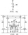
- Fig. 4a shows one way of sensing the differential output common mode.
- the commode mode CMFB is sensed in the middle between two resistances R located between voltages vop and vom.
- Fig. 4b presents a simplified schematic of a common mode regulation circuit 40.
- the part of the circuit signified by 40 of the schematic of Fig. 4b show the common mode regulation circuit as part of the output driver.
- CMFB differential output common mode
- VREF common mode reference
- Fig. 4b allows straightforward insertion of common mode regulation by imbalancing of the tail current of the intermediate stage differential pairs using M13/ M14.
- the main benefit of the class-AB regulation presented is the control of the cross-conducted current inside the amplifier with or without presence of audio signals.
- One additional benefit is to ensure the devices of both output stages remain in linear region to minimize crossover distortion.
- the principle is to sense the current of the device conducting the smallest current, compare it to an internal reference current in order to regulate the minimum current by modulating - in opposite phase - the gate drives of M12/M5 or M6/M11.
- Fig. 5a illustrates how the output stage current sensing could be implemented (half bridge P) in order to generate a voltage IQPFB (respectively IQMFB for half bridge M), which are required to regulate the minimum current by using a differential amplifier 50.
- Fig. 5b depicts a simplified schematic of class-AB feedback (bold lines). It shows an example of quiescent current regulation feedback. The part of the circuit of Fig. 5b regulating the quiescent current is shown with bold lines.
- the error between the two is scaling with feedback voltage IQPFB (respectively IQMFB) voltage and feeding back IQPFB to the active load connected to nodes 1 and 4 then node 1 and 4 voltages will decrease making currents in M5, M8, M0 , and M12 lower the quiescent current.
- IQPFB feedback voltage
- Fig. 6 shows a detailed schematic of the combined implementation of the four control loops.
- the part of the circuit of Fig. 6 regulating the quiescent current is shown with bold lines.
- the part of the circuit of Fig. 6 performing common mode regulation is shown using numeral 40.
- Fig. 6 shows as well how a straightforward Miller compensation of both output branches by capacitors 60-63 can be used to stabilize the four loops as they share the same high impedance nodes 1, 2, 3, and 4.
- MOSCAPS can be used for Miller compensation.
- the MOSCAPS would have to be connected from nodes 1,2,3,4 to ground instead to the outputs as shown in Fig. 6 with capacitors 60-63.
- Fig. 7 shows as well as how a straightforward Miller compensation can be used to stabilize the four loops as they share the same high impedance nodes 1, 2, 3, and 4 as shown in Fig. 6 .
- vip/vim signifies the differential input
- vc signifies the common mode error
- vqp signifies the quiescent current error ( P )
- vqm signifies the quiescent current error ( M ).
- Fig. 8 illustrates a flowchart of a method to achieve a fully differential amplifier operating in class AB mode, comprising an arrangement for differential drive intermediate stage to control a differential loop, a common mode regulation and class AB regulation.
- Step 80 of the method of Fig. 8 illustrates the provision of a fully differential amplifier operating in class AB mode comprising ports for differential input error signals Vip and Vim and for differential output signals Vop and Vom and an output branch for Vop and an output branch for Vom.
- Step 81 depicts enabling output common mode regulation by introducing dual differentiation of the input error signal to support common mode regulation by splitting driving signals for a first transistor of each of said output branch from a control path for a second transistor of each of said output branch.
- Step 82 illustrates that if a differential output common mode is higher than a common mode reference, decreasing voltages of both Vop and Vom, thereby reducing a common mode error and, finally, step 83 illustrates regulating quiescent currents of both output branches inside the amplifier by sensing a current of a device of each output branch conducting the smallest current, comparing it with an internal reference current in order to regulate the minimum current.
- the disclosed architecture allows straightforward insertion of Class-AB regulation by use of feedback to the active load of the same intermediate stage differential pairs.
Landscapes
- Engineering & Computer Science (AREA)
- Power Engineering (AREA)
- Amplifiers (AREA)
Claims (21)
- Un procédé pour réaliser un amplificateur entièrement différentiel fonctionnant en mode de classe AB, comprenant une disposition pour un étage intermédiaire de commande différentielle pour commander une boucle différentielle, une régulation de mode commun et une régulation de classe AB, comprenant les étapes consistant à :(1) fournir un amplificateur entièrement différentiel fonctionnant en classe AB comprenant des ports pour des signaux d'erreur d'entrée différentiels Vip et Vim et pour des signaux de sortie différentiels Vop et Vom, dans lequel Vop est généré par une première branche de sortie (M12, M5) d'un étage de sortie et Vom est généré par une seconde branche de sortie (M11, M6) de l'étage de sortie, dans lequel chacune des branches de sortie comporte des transistors de côté supérieur (M11, M12) et de côté inférieur (M6, M5), dans lequel l'amplificateur comporte un étage intermédiaire traitant les signaux d'entrée :(2) séparer l'étage intermédiaire en deux étages différentiels simples, dans lequel un premier (M1, M2) de ces étages différentiels commande les transistors de côté inférieur (M5, M6) et un second étage différentiel (M3, M4) commande les transistors de côté supérieur (M11, M12), activant ainsi une régulation de sortie différentielle en introduisant une différentiation duale du signal d'erreur d'entrée pour supporter la régulation de mode commun en séparant les signaux de commande d'un premier transistor de chacune desdits branches de sortie à partir d'un chemin de commande d'un second transistor de chacune desdites branches de sortie ;(3) réduire une erreur de mode commun en décroissant les deux tensions Vop et Vom si un mode commun de sortie différentielle (CMFB) est plus élevé qu'une référence de mode commun (VREF), dans lequel une paire de transistors NMOS (M13/M14) compare le mode commun différentiel (CMFB) avec la référence de mode commun (VREF) et réduit l'erreur de mode commun via lesdits premier et second étages différentiels ; et(4) régulier les courants de repos des deux branches de sortie à l'intérieur de l'amplificateur en détectant un courant d'un transistor (M5/M12, M6/M11) de chaque branche de sortie conduisant le plus petit courant, comparant celui-ci avec un courant de référence interne (IREF) afin de régulier le courant de repos, dans lequel ladite régulation du courant de repos est effectuée par la connexion de chaque branche de sortie à une charge active respective et en ramenant un résultat de la comparaison du plus petit courant de chaque transistor (M5/M12, M6/M11) de chaque branche de sortie avec le courant de référence interne (IREF) vers les charges actives respectives, décroissant ainsi les tensions aux noeuds correspondant de chaque branche de sortie et décroissant ainsi les courants de repos.
- Le procédé de la revendication 1 dans lequel l'amplificateur est un amplificateur audio.
- Le procédé de la revendication 1 dans lequel l'étage intermédiaire est divisé en deux étages différentiels simples, l'un (M1, M2) commandant les transistors de côté inférieur (M5, M6) et l'autre (M3, M4) commandant les transistors de côté supérieur (M11, M12), réalisant ainsi ladite division des signaux de commande.
- Le procédé de la revendication 1 dans lequel la tension d'alimentation est séparée entre un rail VDD de l'étage de sortie et une alimentation de l'étage intermédiaire.
- Le procédé de la revendication 4 dans lequel l'étage de sortie est alimenté avec un niveau de tension inférieur à 1V, tandis que l'étage intermédiaire peut être encore alimenté à partir d'une tension supérieure.
- Le procédé de la revendication 1 dans lequel est effectuée une insertion triviale d'une régulation de mode commun au moyen d'un déséquilibre du courant de rail des paires différentielles.
- Le procédé de la revendication 1 dans lequel dans lequel PSR au sein de la bande audio est amélioré en empêchant une alimentation en avance au travers de capacités de compensation.
- Le procédé de la revendication 1 dans lequel est effectuée une insertion triviale d'une régulation de classe AB au moyen d'une utilisation d'une rétroaction vers une charge active de paires différentielles d'un étage intermédiaire.
- Le procédé de la revendication 1 dans lequel une compension de la boucle de régulation principale augmente la stabilité d'une boucle de régulation en mode commun et d'une boucle de régulation en classe AB au moyen de noeuds de haute impédance (1, 2, 3, 4) de la boucle de régulation, la boucle de régulation commune, et la boucle de régulation de classe AB étant partagées.
- Le procédé de la revendication 1 dans lequel une adaptation vers un fonctionnement en classe G peut être réalisé en connecté une alimentation commutée à un étage de puissance.
- Un circuit d'un amplificateur entièrement différentiel fonctionnant en classe AB, comprenant :- un étage de sortie différentiel (Vom, Vop) comprenant une branche P (M12, M5) et une branche M (M11, M6), dans lequel chacune des branches P et M comporte un transistor de côté supérieur (M11, M12) et un transistor de côté inférieur (M6, M5);- un étage intermédiaire différentiel comprenant- une première paire de transistors PMOS (M3/M4) comprenant un premier (M3) et un second (M4) transistor PMOS, qui est capable d'amplifier un signal d'erreur d'entrée différentiel (vip/vim), dans lequel chaque transistor (M3/M4) est capable de générer un signal de commande pour un transistor correspondant parmi lesdits transistors de côté supérieur (M11/M12), dans lequel les sources des deux transistors de la première paire de transistor PMOS sont connectées, dans lequel des sources de courant commandées (21) sont déployées entre chaque drain des transistors de la première paire de transistors PMOS (M3/M4) et la terre,
dans lequel ces sources de courant commandées (21) sont configurées pour être commandées par des erreurs rapportées par des circuits de la boucle de régulation AB ;- une première paire de transistors NMOS (M7/M8) dans laquelle une grille de chaque transistors NMOS (M7/M8) est connectée via un noeud de haute impédance correspondant (3, 4) vers un drain d'un transistor correspondant de la première paire de transistors PMOS (M3/M4) et un drain de chaque transistor NMOS (M7/M8) est connecté à un drain et une grille d'un transistor PMOS correspondant d'une seconde paire de transistors PMOS (M9/M10);- ladite seconde paire de transistors PMOS (M9/M10), dans laquelle chaque grille de la seconde paire de transistors PMOS (M9/M10) est connectée à une grille d'un transistor de côté supérieur correspondant (M11/M12) formant un miroir de courant,
dans lequel chaque transistors PMOS de la seconde paire (M9/M10) de transistors PMOS est réduite suivant une même échelle relative du transistor de côté supérieur ;- une troisième paire de transistors PMOS (M1/M2) comprenant un premier (M1) et un second (M2) transistor PMOS, qui est capable d'amplifier le signal d'erreur d'entrée différentiel (vip/vim) dans lequel chaque transistor (M1 :M2) est capable de générer un signal de commande pour un desdits transistors de côté inférieur correspondant (M5/M6), dans lequel les sources des deux transistors de la troisième paire de transistors PMOS (M1/M2) sont connectées, dans lequel des sources de courant commandées (21) sont déployées entre chaque drain des transistors de la troisième paire de transistors PMOS (M1/M2) et la terre,
dans lequel ces sources de courant commandées (21) sont configurées pour être commandées par des erreurs ramenées par rétroaction des circuits de la boucle de régulation de classe AB ;- un circuit de commande de boucle différentielle comprenant une différentiation duale du signal d'erreur d'entrée différentiel (vip/vim) en séparant l'étage intermédiaire différentiel en deux étages différentiels, dans lequel un premier étage différentiel commande les transistors de côté inférieur (M5, M6) au moyen de la troisième paire de transistors PMOS (M1/M2), dans lequel les grilles des transistors de la troisième paire de transistors PMOS (M1/M2) sont respectivement connectées aux signaux d'entrée vip et vim du signal d'erreur d'entrée différentiel (vip/vim) et dans lequel les grilles des transistors de côté inférieur (M5, M6) sont respectivement connectées aux drains des transistors de la troisième paire de transistors PMOS (M1/M2) via un noeud à haute impédance correspondant (1, 2) et dans lequel un second étage différentiel commande les transistors de côté supérieur (M11 /M12) au moyen de la première paire de transistors PMOS (M3/M4), dans lequel les grilles des transistors de la première paire de transistors PMOS (M3/M4) sont respectivement connectées aux signaux d'entrée vip et vim du signal d'erreur d'entrée différentiel (vip/vim) et dans lequel les grilles des transistors de côté supérieur (M11/M12) sont commandées via les noeuds à haute impédance (3, 4) et un premier transistor NMOS (M7) de la première paire de transistors NMOS (M7/M8) et un premier transistor PMOS (M9) de la seconde paire de transistors NMOS (M9/M10) ou respectivement via un second transistor NMOS (M8) de la première paire de transistors NMOS (M7/M8) et un second transistor PMOS (M10) de la seconde paire de transistors PMOS (M9/M10) ;- un circuit de boucle de régulation de mode commun comprenant :- la troisième paire de transistors PMOS (M1/M2) en parallèle à ladite première paire de transistors PMOS (M3/M4), dans lequel chaque transistor de la troisième paire (M1/M2) de transistors PMOS est capable de commander respectivement l'un desdits transistors de côté inférieur (M5/M6) de la branche de sortie correspondante (branche P/M) via le noeud à haute impédance respectif (1, 2) et chaque transistor de la première paire (M3/M4) de transistors PMOS est capable de commander respectivement une desdits transistors de côté supérieur de la branche de sortie correspondante (branche P/M) (M11/M12) via le noeud à haute impédance respectif (3, 4) dans lequel les sources des deux transistors de la troisième paire de transistors PMOS (M1/M2) sont connectées, et- une seconde paire de transistors NMOS (M13/M14), dans laquelle un drain d'un premier transistor (M13) de la seconde paire de transistors NMOS (M13/M14) est connecté aux sources des transistors de la première paire de transistors PMOS (M3/M4), une grille du premier transistor (M13) est connectée à un retour en mode commun (CMFB) détecté, un drain d'un second transistor (M14) de la seconde paire de transistors NMOS (M13/M14) est connecté aux sources des transistors de la troisième paire de transistors PMOS (M1/M2), et une grille du second transistor (M14) est connectée au potentiel de référence de mode commun (VREF) ;
dans lequel une compensation de fréquence du circuit de commande de boucle différentielle et du circuit de régulation du mode commun est partagé au moyen d'un partage des noeuds à haute impédance (1, 2, 3, 4) du circuit de commande de boucle différentielle et du circuit de régulation de mode commun ; et- lesdits circuits de boucle de régulation de classe AB, dans lequel un premier circuit parmi lesdits circuits de boucle de régulation de classe AB est configuré pour fournir une tension (IQPFB) aux noeuds à haute impédance (1, 4) configurés pour commander la branche P (M12, M5), dans lequel la tension (IQPFB) est configurée pour ramener à l'échelle une erreur de courant de repos de la branche P (M12, M5), dans lequel l'erreur de courant de repos de la branche P est la différent du plus petit courant parmi les courants s'écoulant respectivement au travers le transistor de côté supérieur (M12) ou le transistor de côté inférieur (M5) de la branche P en comparaison avec un courant de référence interne,afin de réguler le plus petit courant au moyen d'une modulation en opposition de phase, la grille commande le transistor de côté supérieur (M12) et le transistor de côté inférieur (M5) de la branche P via lesdits noeuds à haute impédance (4, 1) configurés pour commander la branche P et le second transistor NMOS (M8) de la première paire de transistors NMOS (M7/M8) et le second transistor PMOS (M10) de la seconde paire de transistor PMOS (M9/M10) ; et dans lequel un circuit parmi lesdits circuits de boucle de régulation de classe AB est configuré pour fournir une tension (IQMFB) aux noeuds à haute impédance (2, 3) configurés pour commander la branche M (M11, M6), dans lequel la tension (IQMFB) est configurée pour ramener à l'échelle une erreur de courant de repos de la branche M (M12, M5), dans lequel l'erreur de courant de repos de la branche M est la différence du plus petit courant parmi les courants s'écoulant via le transistor de côté supérieur (M11) ou le transistor de côté inférieur (M6) de la branche M en comparaison avec le courant de référence interne,
afin de réguler le plus petit courant par une modulation en opposition de phase, la grille commande le transistor de côté supérieur (M11) et le transistor de côté inférieur (M6) de la branche M via lesdits noeuds à haute impédance (3, 2) configurés pour commander la branche M et le premier transistor NMOS (M7) de la première paire de transistors NMOS (M7/M8) et le premier transistor PMOS (M9) de la seconde paire de transistors PMOS (M9 /M10). - Le circuit de la revendication 11 dans lequel l'amplificateur fonctionne en tant qu'amplificateur audio.
- Le circuit de la revendication 11 dans lequel l'étage de sortie est configuré pour être alimenté par une tension inférieure à 1 volt.
- Le circuit de la revendication 11 dans lequel l'étage intermédiaire est configuré pour être alimenté par une tension qui est supérieure à une tension d'alimentation de l'étage de sortie.
- Le circuit de la revendication 11 dans lequel les noeuds à haute impédance (1, 2, 3, 4) sont partagés avec les noeuds à haute impédance de la boucle de régulation en mode commun permettant le partage de la compensation de fréquence des deux boucles.
- Le circuit de la revendication 11 dans lequel, afin de permettre la compensation de fréquence, une capacité (60, 61) est connectée entre la branche M (M11, M6) et chacun des noeuds à haute impédance (2, 3) commandant la branche M et une capacité (62, 69) est connectée entre la branche P (M5, M12) et chacun des noeuds à haute impédance (1, 4) capable de commander la branche P (M5, M12).
- Le circuit de la revendication 11 dans lequel, afin de permettre la compensation de fréquence, une capacité MOS est connectée entre la terre et chaque noeuds à haute impédance (2, 3) capable de commander la branche M (M11 ; M7) et une capacité MOS est connectée entre la terre et chacun des noeuds à haute impédance (1, 4) commandant la branche P (M5, M12).
- Le circuit de la revendication 11 dans lequel toutes les boucles de régulation partagent les quatres noeuds à haute impédance (1, 2, 3, 4).
- Le circuit de la revendication 11 dans lequel le circuit est capable d'une insertion d'une régulation en mode commun en étant configuré pour un déséquilibre du courant de queue de la seconde paire différentielle de transistors NMOS (M13/M14) de l'étage intermédiaire.
- Le circuit de la revendication 11 dans lequel dans lequel la régulation de classe AB est configurée pour ramener la tension de retour (IQPFB) à une charge active connectée aux noeuds à haute impédance relatifs (1, 4), dans lequel les tensions des noeuds à haute impédance relatifs (1, 4) décroissent et réduisent en conséquence les courants de repos du transistor de côté supérieur (M12) et du transistor de côté inférieur (M8) de la première paire de transistors NMOS (M7/M8) et dans le second transistor PMOS (M10) de la seconde paire de transistors PMOS (M9/M10) ;
et est en outre configuré pour ramener en retour le potentiel de retour (IQFMB) à une charge active connectée aux noeuds à haute impédance relatifs (2, 3), dans lequel les tensions des noeuds à haute impédance relatifs (2, 3) décroissent et ainsi réduisent les courants de repos dans le transistor de côté supérieur (M11) et le transistor de côté inférieur (M6) de la branche M, dans le premier transistor NMOS (M7) de la première paire de transistors NMOS (M7/M8) et dans le premier transistor PMOS (M9) de la seconde paire de transistors PMOS (M9/M10). - Le circuit de la revendication 11 dans lequel le circuit est capable d'adaptation à un fonctionnement en classe G via une connexion de l'étage de puissance à une alimentation commutée.
Priority Applications (2)
| Application Number | Priority Date | Filing Date | Title |
|---|---|---|---|
| EP12368006.8A EP2645565B1 (fr) | 2012-03-27 | 2012-03-27 | Topologie d'amplificateur entièrement différentiel pour entraîner des haut-parleurs dynamiques en mode de classe AB |
| US13/433,900 US8674765B2 (en) | 2012-03-27 | 2012-03-29 | Fully differential amplifier topology to drive dynamic speakers in class AB mode |
Applications Claiming Priority (1)
| Application Number | Priority Date | Filing Date | Title |
|---|---|---|---|
| EP12368006.8A EP2645565B1 (fr) | 2012-03-27 | 2012-03-27 | Topologie d'amplificateur entièrement différentiel pour entraîner des haut-parleurs dynamiques en mode de classe AB |
Publications (2)
| Publication Number | Publication Date |
|---|---|
| EP2645565A1 EP2645565A1 (fr) | 2013-10-02 |
| EP2645565B1 true EP2645565B1 (fr) | 2019-03-06 |
Family
ID=45992149
Family Applications (1)
| Application Number | Title | Priority Date | Filing Date |
|---|---|---|---|
| EP12368006.8A Active EP2645565B1 (fr) | 2012-03-27 | 2012-03-27 | Topologie d'amplificateur entièrement différentiel pour entraîner des haut-parleurs dynamiques en mode de classe AB |
Country Status (2)
| Country | Link |
|---|---|
| US (1) | US8674765B2 (fr) |
| EP (1) | EP2645565B1 (fr) |
Families Citing this family (12)
| Publication number | Priority date | Publication date | Assignee | Title |
|---|---|---|---|---|
| US8988063B2 (en) * | 2012-04-10 | 2015-03-24 | Maxim Integrated Products, Inc. | System and method for current measurement in the presence of high common mode voltages |
| US8902003B2 (en) * | 2012-12-17 | 2014-12-02 | Intel Mobile Communications GmbH | Amplifier, mobile communication device and method for amplifying |
| US8928406B2 (en) * | 2013-03-13 | 2015-01-06 | Texas Instruments Incorporated | Low-power inverter-based differential amplifier |
| DK2963814T3 (en) * | 2014-07-03 | 2018-11-12 | Bang & Olufsen As | Class AB amplifier with bias control |
| CN104639076B (zh) * | 2014-08-27 | 2018-12-11 | 北京中电华大电子设计有限责任公司 | 一种低功耗的宽带全差分运算放大器 |
| KR20170003025A (ko) * | 2015-06-30 | 2017-01-09 | 에스케이하이닉스 주식회사 | 내부전압 생성회로 |
| KR102446880B1 (ko) * | 2015-08-17 | 2022-09-26 | 삼성디스플레이 주식회사 | 표시 장치 및 이의 구동 방법 |
| TWI720773B (zh) * | 2020-01-08 | 2021-03-01 | 益力半導體股份有限公司 | 低輸入阻抗式電流取樣保持電路模組及二加一階三角積分類比數位轉換器 |
| US11671094B1 (en) | 2021-01-11 | 2023-06-06 | Dialog Semiconductor (Uk) Limited | Driver circuit |
| US11457307B2 (en) | 2021-02-23 | 2022-09-27 | Macronix Iniernational Co., Ltd. | Headphone driver and driving method thereof |
| TWI789712B (zh) * | 2021-02-23 | 2023-01-11 | 旺宏電子股份有限公司 | 耳機驅動器及驅動方法 |
| DE102022205384A1 (de) | 2022-05-30 | 2023-11-30 | Robert Bosch Gesellschaft mit beschränkter Haftung | Ansteuerschaltung für einen mikroelektromechanischen Schallerzeuger und Schallerzeugungssystem |
Family Cites Families (8)
| Publication number | Priority date | Publication date | Assignee | Title |
|---|---|---|---|---|
| CA2050878C (fr) * | 1991-09-06 | 1999-10-19 | Gerald Molnar | Amplificateur de puissance a commande du courant de repos |
| US6642788B1 (en) * | 2001-11-05 | 2003-11-04 | Xilinx, Inc. | Differential cascode amplifier |
| KR100620662B1 (ko) | 2003-09-26 | 2006-09-19 | 엔이씨 일렉트로닉스 가부시키가이샤 | 차동 에이비 클래스 증폭 회로 및 이를 이용한 구동 회로 |
| US7315204B2 (en) | 2005-07-08 | 2008-01-01 | National Semiconductor Corporation | Class AB-D audio power amplifier |
| WO2009063276A1 (fr) * | 2007-11-15 | 2009-05-22 | Freescale Semiconductor, Inc. | Circuit amplificateur |
| JP5075051B2 (ja) | 2008-08-05 | 2012-11-14 | ルネサスエレクトロニクス株式会社 | Ab級増幅回路、及び表示装置 |
| US7999619B2 (en) | 2009-02-09 | 2011-08-16 | Infineon Technologies Ag | Class AB output stage |
| US7898330B2 (en) | 2009-04-21 | 2011-03-01 | Number 14 B.V. | Class AB amplifier systems |
-
2012
- 2012-03-27 EP EP12368006.8A patent/EP2645565B1/fr active Active
- 2012-03-29 US US13/433,900 patent/US8674765B2/en active Active
Non-Patent Citations (2)
| Title |
|---|
| LOPEZ-MORILLO E ET AL: "A Very Low-Power Class AB/AB Op-amp based Sigma-Delta Modulator for Biomedical Applications", CIRCUITS AND SYSTEMS, 2006. MWSCAS '06. 49TH IEEE INTERNATIONAL MIDWES T SYMPOSIUM ON, IEEE, PI, 1 August 2006 (2006-08-01), pages 458 - 462, XP031113639, ISBN: 978-1-4244-0172-7 * |
| THOUTAM S ET AL: "Power efficient fully differential low-voltage two stage class AB/AB op-amp architectures", PROCEEDINGS / 2004 IEEE INTERNATIONAL SYMPOSIUM ON CIRCUITS AND SYSTEMS : MAY 23 - 26, 2004, SHERATON VANCOUVER WALL CENTRE HOTEL, VANCOUVER, BRITISH COLUMBIA, CANADA, IEEE OPERATIONS CENTER, PISCATAWAY, NJ, 23 May 2004 (2004-05-23), pages I - 733, XP010719437, ISBN: 978-0-7803-8251-0 * |
Also Published As
| Publication number | Publication date |
|---|---|
| US8674765B2 (en) | 2014-03-18 |
| EP2645565A1 (fr) | 2013-10-02 |
| US20130257535A1 (en) | 2013-10-03 |
Similar Documents
| Publication | Publication Date | Title |
|---|---|---|
| EP2645565B1 (fr) | Topologie d'amplificateur entièrement différentiel pour entraîner des haut-parleurs dynamiques en mode de classe AB | |
| US8552801B2 (en) | Amplifier common-mode control methods | |
| US6556081B2 (en) | Single-ended, ultra low voltage class AB power amplifier architecture having a common-mode feedback quiescent current control circuit | |
| JP2001230637A (ja) | 低電圧形の広帯域演算増幅器 | |
| US6476674B2 (en) | Method and apparatus for error correction of amplifier | |
| US9973156B2 (en) | Generation of voltage reference signals in a hybrid switched mode amplifier | |
| GB2546576A (en) | Hybrid switched mode amplifier | |
| US7253685B2 (en) | Class AB amplifier having adjustable quiescent current and output current | |
| EP4040674B1 (fr) | Circuit d'amplification avec compensation de fluctuation de tension en mode commun | |
| US6307430B1 (en) | Noise reduction technique in chopper stabilized amplifier | |
| EP4064559A1 (fr) | Compensation active de mode commun pour une meilleure performance d'amplificateur | |
| JP2002198752A (ja) | 超低電圧cmosのab級電力増幅器 | |
| US8400214B2 (en) | Class AB output stage | |
| CN121710830A (zh) | 用于测量连接到功率放大器的负载的电压和电流感测电路 | |
| JP4015237B2 (ja) | 低ノイズ増幅器構造体 | |
| US11885836B2 (en) | Voltage-to-current architecture and error | |
| Dessouky et al. | Very low-voltage fully differential amplifier for switched-capacitor applications | |
| Carrillo et al. | 1-V rail-to-rail bulk-driven CMOS OTA with enhanced gain and gain-bandwidth product | |
| Castello | CMOS buffer amplifiers | |
| US5497122A (en) | Low power class-AB integrated circuit amplifier | |
| US5825244A (en) | Low power class AB integrated circuit amplifier having improved linearity when driving high impedance loads | |
| CN105122640B (zh) | 用于ab类放大器的输出级 | |
| US7202746B1 (en) | Multiple-stage operational amplifier and methods and systems utilizing the same | |
| US20050013029A1 (en) | Voice coil motor power amplifier | |
| US7567125B2 (en) | Differential amplifier with multiple signal gains and wide dynamic range |
Legal Events
| Date | Code | Title | Description |
|---|---|---|---|
| PUAI | Public reference made under article 153(3) epc to a published international application that has entered the european phase |
Free format text: ORIGINAL CODE: 0009012 |
|
| AK | Designated contracting states |
Kind code of ref document: A1 Designated state(s): AL AT BE BG CH CY CZ DE DK EE ES FI FR GB GR HR HU IE IS IT LI LT LU LV MC MK MT NL NO PL PT RO RS SE SI SK SM TR |
|
| AX | Request for extension of the european patent |
Extension state: BA ME |
|
| 17P | Request for examination filed |
Effective date: 20140329 |
|
| RBV | Designated contracting states (corrected) |
Designated state(s): AL AT BE BG CH CY CZ DE DK EE ES FI FR GB GR HR HU IE IS IT LI LT LU LV MC MK MT NL NO PL PT RO RS SE SI SK SM TR |
|
| STAA | Information on the status of an ep patent application or granted ep patent |
Free format text: STATUS: EXAMINATION IS IN PROGRESS |
|
| 17Q | First examination report despatched |
Effective date: 20180205 |
|
| GRAP | Despatch of communication of intention to grant a patent |
Free format text: ORIGINAL CODE: EPIDOSNIGR1 |
|
| STAA | Information on the status of an ep patent application or granted ep patent |
Free format text: STATUS: GRANT OF PATENT IS INTENDED |
|
| INTG | Intention to grant announced |
Effective date: 20180906 |
|
| GRAS | Grant fee paid |
Free format text: ORIGINAL CODE: EPIDOSNIGR3 |
|
| GRAA | (expected) grant |
Free format text: ORIGINAL CODE: 0009210 |
|
| STAA | Information on the status of an ep patent application or granted ep patent |
Free format text: STATUS: THE PATENT HAS BEEN GRANTED |
|
| AK | Designated contracting states |
Kind code of ref document: B1 Designated state(s): AL AT BE BG CH CY CZ DE DK EE ES FI FR GB GR HR HU IE IS IT LI LT LU LV MC MK MT NL NO PL PT RO RS SE SI SK SM TR |
|
| REG | Reference to a national code |
Ref country code: GB Ref legal event code: FG4D |
|
| REG | Reference to a national code |
Ref country code: CH Ref legal event code: EP Ref country code: AT Ref legal event code: REF Ref document number: 1105926 Country of ref document: AT Kind code of ref document: T Effective date: 20190315 |
|
| REG | Reference to a national code |
Ref country code: DE Ref legal event code: R096 Ref document number: 602012057396 Country of ref document: DE |
|
| REG | Reference to a national code |
Ref country code: IE Ref legal event code: FG4D |
|
| REG | Reference to a national code |
Ref country code: NL Ref legal event code: MP Effective date: 20190306 |
|
| REG | Reference to a national code |
Ref country code: LT Ref legal event code: MG4D |
|
| PG25 | Lapsed in a contracting state [announced via postgrant information from national office to epo] |
Ref country code: LT Free format text: LAPSE BECAUSE OF FAILURE TO SUBMIT A TRANSLATION OF THE DESCRIPTION OR TO PAY THE FEE WITHIN THE PRESCRIBED TIME-LIMIT Effective date: 20190306 Ref country code: FI Free format text: LAPSE BECAUSE OF FAILURE TO SUBMIT A TRANSLATION OF THE DESCRIPTION OR TO PAY THE FEE WITHIN THE PRESCRIBED TIME-LIMIT Effective date: 20190306 Ref country code: SE Free format text: LAPSE BECAUSE OF FAILURE TO SUBMIT A TRANSLATION OF THE DESCRIPTION OR TO PAY THE FEE WITHIN THE PRESCRIBED TIME-LIMIT Effective date: 20190306 Ref country code: NO Free format text: LAPSE BECAUSE OF FAILURE TO SUBMIT A TRANSLATION OF THE DESCRIPTION OR TO PAY THE FEE WITHIN THE PRESCRIBED TIME-LIMIT Effective date: 20190606 |
|
| PG25 | Lapsed in a contracting state [announced via postgrant information from national office to epo] |
Ref country code: LV Free format text: LAPSE BECAUSE OF FAILURE TO SUBMIT A TRANSLATION OF THE DESCRIPTION OR TO PAY THE FEE WITHIN THE PRESCRIBED TIME-LIMIT Effective date: 20190306 Ref country code: GR Free format text: LAPSE BECAUSE OF FAILURE TO SUBMIT A TRANSLATION OF THE DESCRIPTION OR TO PAY THE FEE WITHIN THE PRESCRIBED TIME-LIMIT Effective date: 20190607 Ref country code: HR Free format text: LAPSE BECAUSE OF FAILURE TO SUBMIT A TRANSLATION OF THE DESCRIPTION OR TO PAY THE FEE WITHIN THE PRESCRIBED TIME-LIMIT Effective date: 20190306 Ref country code: RS Free format text: LAPSE BECAUSE OF FAILURE TO SUBMIT A TRANSLATION OF THE DESCRIPTION OR TO PAY THE FEE WITHIN THE PRESCRIBED TIME-LIMIT Effective date: 20190306 Ref country code: BG Free format text: LAPSE BECAUSE OF FAILURE TO SUBMIT A TRANSLATION OF THE DESCRIPTION OR TO PAY THE FEE WITHIN THE PRESCRIBED TIME-LIMIT Effective date: 20190606 Ref country code: NL Free format text: LAPSE BECAUSE OF FAILURE TO SUBMIT A TRANSLATION OF THE DESCRIPTION OR TO PAY THE FEE WITHIN THE PRESCRIBED TIME-LIMIT Effective date: 20190306 |
|
| REG | Reference to a national code |
Ref country code: AT Ref legal event code: MK05 Ref document number: 1105926 Country of ref document: AT Kind code of ref document: T Effective date: 20190306 |
|
| PG25 | Lapsed in a contracting state [announced via postgrant information from national office to epo] |
Ref country code: ES Free format text: LAPSE BECAUSE OF FAILURE TO SUBMIT A TRANSLATION OF THE DESCRIPTION OR TO PAY THE FEE WITHIN THE PRESCRIBED TIME-LIMIT Effective date: 20190306 Ref country code: PT Free format text: LAPSE BECAUSE OF FAILURE TO SUBMIT A TRANSLATION OF THE DESCRIPTION OR TO PAY THE FEE WITHIN THE PRESCRIBED TIME-LIMIT Effective date: 20190706 Ref country code: AL Free format text: LAPSE BECAUSE OF FAILURE TO SUBMIT A TRANSLATION OF THE DESCRIPTION OR TO PAY THE FEE WITHIN THE PRESCRIBED TIME-LIMIT Effective date: 20190306 Ref country code: CZ Free format text: LAPSE BECAUSE OF FAILURE TO SUBMIT A TRANSLATION OF THE DESCRIPTION OR TO PAY THE FEE WITHIN THE PRESCRIBED TIME-LIMIT Effective date: 20190306 Ref country code: RO Free format text: LAPSE BECAUSE OF FAILURE TO SUBMIT A TRANSLATION OF THE DESCRIPTION OR TO PAY THE FEE WITHIN THE PRESCRIBED TIME-LIMIT Effective date: 20190306 Ref country code: SK Free format text: LAPSE BECAUSE OF FAILURE TO SUBMIT A TRANSLATION OF THE DESCRIPTION OR TO PAY THE FEE WITHIN THE PRESCRIBED TIME-LIMIT Effective date: 20190306 Ref country code: EE Free format text: LAPSE BECAUSE OF FAILURE TO SUBMIT A TRANSLATION OF THE DESCRIPTION OR TO PAY THE FEE WITHIN THE PRESCRIBED TIME-LIMIT Effective date: 20190306 Ref country code: IT Free format text: LAPSE BECAUSE OF FAILURE TO SUBMIT A TRANSLATION OF THE DESCRIPTION OR TO PAY THE FEE WITHIN THE PRESCRIBED TIME-LIMIT Effective date: 20190306 |
|
| REG | Reference to a national code |
Ref country code: CH Ref legal event code: PL |
|
| PG25 | Lapsed in a contracting state [announced via postgrant information from national office to epo] |
Ref country code: PL Free format text: LAPSE BECAUSE OF FAILURE TO SUBMIT A TRANSLATION OF THE DESCRIPTION OR TO PAY THE FEE WITHIN THE PRESCRIBED TIME-LIMIT Effective date: 20190306 Ref country code: SM Free format text: LAPSE BECAUSE OF FAILURE TO SUBMIT A TRANSLATION OF THE DESCRIPTION OR TO PAY THE FEE WITHIN THE PRESCRIBED TIME-LIMIT Effective date: 20190306 Ref country code: LU Free format text: LAPSE BECAUSE OF NON-PAYMENT OF DUE FEES Effective date: 20190327 |
|
| REG | Reference to a national code |
Ref country code: BE Ref legal event code: MM Effective date: 20190331 |
|
| REG | Reference to a national code |
Ref country code: DE Ref legal event code: R097 Ref document number: 602012057396 Country of ref document: DE |
|
| PG25 | Lapsed in a contracting state [announced via postgrant information from national office to epo] |
Ref country code: IS Free format text: LAPSE BECAUSE OF FAILURE TO SUBMIT A TRANSLATION OF THE DESCRIPTION OR TO PAY THE FEE WITHIN THE PRESCRIBED TIME-LIMIT Effective date: 20190706 Ref country code: AT Free format text: LAPSE BECAUSE OF FAILURE TO SUBMIT A TRANSLATION OF THE DESCRIPTION OR TO PAY THE FEE WITHIN THE PRESCRIBED TIME-LIMIT Effective date: 20190306 |
|
| PLBE | No opposition filed within time limit |
Free format text: ORIGINAL CODE: 0009261 |
|
| STAA | Information on the status of an ep patent application or granted ep patent |
Free format text: STATUS: NO OPPOSITION FILED WITHIN TIME LIMIT |
|
| PG25 | Lapsed in a contracting state [announced via postgrant information from national office to epo] |
Ref country code: DK Free format text: LAPSE BECAUSE OF FAILURE TO SUBMIT A TRANSLATION OF THE DESCRIPTION OR TO PAY THE FEE WITHIN THE PRESCRIBED TIME-LIMIT Effective date: 20190306 Ref country code: CH Free format text: LAPSE BECAUSE OF NON-PAYMENT OF DUE FEES Effective date: 20190331 Ref country code: IE Free format text: LAPSE BECAUSE OF NON-PAYMENT OF DUE FEES Effective date: 20190327 Ref country code: MC Free format text: LAPSE BECAUSE OF FAILURE TO SUBMIT A TRANSLATION OF THE DESCRIPTION OR TO PAY THE FEE WITHIN THE PRESCRIBED TIME-LIMIT Effective date: 20190306 Ref country code: LI Free format text: LAPSE BECAUSE OF NON-PAYMENT OF DUE FEES Effective date: 20190331 |
|
| 26N | No opposition filed |
Effective date: 20191209 |
|
| PG25 | Lapsed in a contracting state [announced via postgrant information from national office to epo] |
Ref country code: SI Free format text: LAPSE BECAUSE OF FAILURE TO SUBMIT A TRANSLATION OF THE DESCRIPTION OR TO PAY THE FEE WITHIN THE PRESCRIBED TIME-LIMIT Effective date: 20190306 Ref country code: BE Free format text: LAPSE BECAUSE OF NON-PAYMENT OF DUE FEES Effective date: 20190331 |
|
| PG25 | Lapsed in a contracting state [announced via postgrant information from national office to epo] |
Ref country code: TR Free format text: LAPSE BECAUSE OF FAILURE TO SUBMIT A TRANSLATION OF THE DESCRIPTION OR TO PAY THE FEE WITHIN THE PRESCRIBED TIME-LIMIT Effective date: 20190306 |
|
| PG25 | Lapsed in a contracting state [announced via postgrant information from national office to epo] |
Ref country code: FR Free format text: LAPSE BECAUSE OF NON-PAYMENT OF DUE FEES Effective date: 20190506 Ref country code: MT Free format text: LAPSE BECAUSE OF NON-PAYMENT OF DUE FEES Effective date: 20190327 |
|
| PG25 | Lapsed in a contracting state [announced via postgrant information from national office to epo] |
Ref country code: CY Free format text: LAPSE BECAUSE OF FAILURE TO SUBMIT A TRANSLATION OF THE DESCRIPTION OR TO PAY THE FEE WITHIN THE PRESCRIBED TIME-LIMIT Effective date: 20190306 |
|
| PG25 | Lapsed in a contracting state [announced via postgrant information from national office to epo] |
Ref country code: HU Free format text: LAPSE BECAUSE OF FAILURE TO SUBMIT A TRANSLATION OF THE DESCRIPTION OR TO PAY THE FEE WITHIN THE PRESCRIBED TIME-LIMIT; INVALID AB INITIO Effective date: 20120327 |
|
| PG25 | Lapsed in a contracting state [announced via postgrant information from national office to epo] |
Ref country code: MK Free format text: LAPSE BECAUSE OF FAILURE TO SUBMIT A TRANSLATION OF THE DESCRIPTION OR TO PAY THE FEE WITHIN THE PRESCRIBED TIME-LIMIT Effective date: 20190306 |
|
| PGFP | Annual fee paid to national office [announced via postgrant information from national office to epo] |
Ref country code: GB Payment date: 20260310 Year of fee payment: 15 |
|
| PGFP | Annual fee paid to national office [announced via postgrant information from national office to epo] |
Ref country code: DE Payment date: 20260304 Year of fee payment: 15 |