EP2650722B1 - Dispositif d'affichage à cristaux liquides - Google Patents
Dispositif d'affichage à cristaux liquides Download PDFInfo
- Publication number
- EP2650722B1 EP2650722B1 EP11847849.4A EP11847849A EP2650722B1 EP 2650722 B1 EP2650722 B1 EP 2650722B1 EP 11847849 A EP11847849 A EP 11847849A EP 2650722 B1 EP2650722 B1 EP 2650722B1
- Authority
- EP
- European Patent Office
- Prior art keywords
- electrode
- pixel
- liquid crystal
- sub
- pixels
- Prior art date
- Legal status (The legal status is an assumption and is not a legal conclusion. Google has not performed a legal analysis and makes no representation as to the accuracy of the status listed.)
- Not-in-force
Links
Images







Classifications
-
- G—PHYSICS
- G02—OPTICS
- G02F—OPTICAL DEVICES OR ARRANGEMENTS FOR THE CONTROL OF LIGHT BY MODIFICATION OF THE OPTICAL PROPERTIES OF THE MEDIA OF THE ELEMENTS INVOLVED THEREIN; NON-LINEAR OPTICS; FREQUENCY-CHANGING OF LIGHT; OPTICAL LOGIC ELEMENTS; OPTICAL ANALOGUE/DIGITAL CONVERTERS
- G02F1/00—Devices or arrangements for the control of the intensity, colour, phase, polarisation or direction of light arriving from an independent light source, e.g. switching, gating or modulating; Non-linear optics
- G02F1/01—Devices or arrangements for the control of the intensity, colour, phase, polarisation or direction of light arriving from an independent light source, e.g. switching, gating or modulating; Non-linear optics for the control of the intensity, phase, polarisation or colour
- G02F1/13—Devices or arrangements for the control of the intensity, colour, phase, polarisation or direction of light arriving from an independent light source, e.g. switching, gating or modulating; Non-linear optics for the control of the intensity, phase, polarisation or colour based on liquid crystals, e.g. single liquid crystal display cells
- G02F1/133—Constructional arrangements; Operation of liquid crystal cells; Circuit arrangements
- G02F1/1333—Constructional arrangements; Manufacturing methods
- G02F1/1337—Surface-induced orientation of the liquid crystal molecules, e.g. by alignment layers
- G02F1/133707—Structures for producing distorted electric fields, e.g. bumps, protrusions, recesses, slits in pixel electrodes
-
- G—PHYSICS
- G02—OPTICS
- G02F—OPTICAL DEVICES OR ARRANGEMENTS FOR THE CONTROL OF LIGHT BY MODIFICATION OF THE OPTICAL PROPERTIES OF THE MEDIA OF THE ELEMENTS INVOLVED THEREIN; NON-LINEAR OPTICS; FREQUENCY-CHANGING OF LIGHT; OPTICAL LOGIC ELEMENTS; OPTICAL ANALOGUE/DIGITAL CONVERTERS
- G02F1/00—Devices or arrangements for the control of the intensity, colour, phase, polarisation or direction of light arriving from an independent light source, e.g. switching, gating or modulating; Non-linear optics
- G02F1/01—Devices or arrangements for the control of the intensity, colour, phase, polarisation or direction of light arriving from an independent light source, e.g. switching, gating or modulating; Non-linear optics for the control of the intensity, phase, polarisation or colour
- G02F1/13—Devices or arrangements for the control of the intensity, colour, phase, polarisation or direction of light arriving from an independent light source, e.g. switching, gating or modulating; Non-linear optics for the control of the intensity, phase, polarisation or colour based on liquid crystals, e.g. single liquid crystal display cells
- G02F1/133—Constructional arrangements; Operation of liquid crystal cells; Circuit arrangements
- G02F1/1333—Constructional arrangements; Manufacturing methods
- G02F1/1337—Surface-induced orientation of the liquid crystal molecules, e.g. by alignment layers
- G02F1/133742—Surface-induced orientation of the liquid crystal molecules, e.g. by alignment layers for homeotropic alignment
-
- G—PHYSICS
- G02—OPTICS
- G02F—OPTICAL DEVICES OR ARRANGEMENTS FOR THE CONTROL OF LIGHT BY MODIFICATION OF THE OPTICAL PROPERTIES OF THE MEDIA OF THE ELEMENTS INVOLVED THEREIN; NON-LINEAR OPTICS; FREQUENCY-CHANGING OF LIGHT; OPTICAL LOGIC ELEMENTS; OPTICAL ANALOGUE/DIGITAL CONVERTERS
- G02F1/00—Devices or arrangements for the control of the intensity, colour, phase, polarisation or direction of light arriving from an independent light source, e.g. switching, gating or modulating; Non-linear optics
- G02F1/01—Devices or arrangements for the control of the intensity, colour, phase, polarisation or direction of light arriving from an independent light source, e.g. switching, gating or modulating; Non-linear optics for the control of the intensity, phase, polarisation or colour
- G02F1/13—Devices or arrangements for the control of the intensity, colour, phase, polarisation or direction of light arriving from an independent light source, e.g. switching, gating or modulating; Non-linear optics for the control of the intensity, phase, polarisation or colour based on liquid crystals, e.g. single liquid crystal display cells
- G02F1/133—Constructional arrangements; Operation of liquid crystal cells; Circuit arrangements
- G02F1/1333—Constructional arrangements; Manufacturing methods
- G02F1/1343—Electrodes
- G02F1/134309—Electrodes characterised by their geometrical arrangement
-
- G—PHYSICS
- G02—OPTICS
- G02F—OPTICAL DEVICES OR ARRANGEMENTS FOR THE CONTROL OF LIGHT BY MODIFICATION OF THE OPTICAL PROPERTIES OF THE MEDIA OF THE ELEMENTS INVOLVED THEREIN; NON-LINEAR OPTICS; FREQUENCY-CHANGING OF LIGHT; OPTICAL LOGIC ELEMENTS; OPTICAL ANALOGUE/DIGITAL CONVERTERS
- G02F1/00—Devices or arrangements for the control of the intensity, colour, phase, polarisation or direction of light arriving from an independent light source, e.g. switching, gating or modulating; Non-linear optics
- G02F1/01—Devices or arrangements for the control of the intensity, colour, phase, polarisation or direction of light arriving from an independent light source, e.g. switching, gating or modulating; Non-linear optics for the control of the intensity, phase, polarisation or colour
- G02F1/13—Devices or arrangements for the control of the intensity, colour, phase, polarisation or direction of light arriving from an independent light source, e.g. switching, gating or modulating; Non-linear optics for the control of the intensity, phase, polarisation or colour based on liquid crystals, e.g. single liquid crystal display cells
- G02F1/133—Constructional arrangements; Operation of liquid crystal cells; Circuit arrangements
- G02F1/1333—Constructional arrangements; Manufacturing methods
- G02F1/1343—Electrodes
- G02F1/134309—Electrodes characterised by their geometrical arrangement
- G02F1/134318—Electrodes characterised by their geometrical arrangement having a patterned common electrode
-
- G—PHYSICS
- G02—OPTICS
- G02F—OPTICAL DEVICES OR ARRANGEMENTS FOR THE CONTROL OF LIGHT BY MODIFICATION OF THE OPTICAL PROPERTIES OF THE MEDIA OF THE ELEMENTS INVOLVED THEREIN; NON-LINEAR OPTICS; FREQUENCY-CHANGING OF LIGHT; OPTICAL LOGIC ELEMENTS; OPTICAL ANALOGUE/DIGITAL CONVERTERS
- G02F1/00—Devices or arrangements for the control of the intensity, colour, phase, polarisation or direction of light arriving from an independent light source, e.g. switching, gating or modulating; Non-linear optics
- G02F1/01—Devices or arrangements for the control of the intensity, colour, phase, polarisation or direction of light arriving from an independent light source, e.g. switching, gating or modulating; Non-linear optics for the control of the intensity, phase, polarisation or colour
- G02F1/13—Devices or arrangements for the control of the intensity, colour, phase, polarisation or direction of light arriving from an independent light source, e.g. switching, gating or modulating; Non-linear optics for the control of the intensity, phase, polarisation or colour based on liquid crystals, e.g. single liquid crystal display cells
- G02F1/133—Constructional arrangements; Operation of liquid crystal cells; Circuit arrangements
- G02F1/1333—Constructional arrangements; Manufacturing methods
- G02F1/1343—Electrodes
- G02F1/134309—Electrodes characterised by their geometrical arrangement
- G02F1/134381—Hybrid switching mode, i.e. for applying an electric field with components parallel and orthogonal to the substrates
-
- G—PHYSICS
- G02—OPTICS
- G02F—OPTICAL DEVICES OR ARRANGEMENTS FOR THE CONTROL OF LIGHT BY MODIFICATION OF THE OPTICAL PROPERTIES OF THE MEDIA OF THE ELEMENTS INVOLVED THEREIN; NON-LINEAR OPTICS; FREQUENCY-CHANGING OF LIGHT; OPTICAL LOGIC ELEMENTS; OPTICAL ANALOGUE/DIGITAL CONVERTERS
- G02F1/00—Devices or arrangements for the control of the intensity, colour, phase, polarisation or direction of light arriving from an independent light source, e.g. switching, gating or modulating; Non-linear optics
- G02F1/01—Devices or arrangements for the control of the intensity, colour, phase, polarisation or direction of light arriving from an independent light source, e.g. switching, gating or modulating; Non-linear optics for the control of the intensity, phase, polarisation or colour
- G02F1/13—Devices or arrangements for the control of the intensity, colour, phase, polarisation or direction of light arriving from an independent light source, e.g. switching, gating or modulating; Non-linear optics for the control of the intensity, phase, polarisation or colour based on liquid crystals, e.g. single liquid crystal display cells
- G02F1/137—Devices or arrangements for the control of the intensity, colour, phase, polarisation or direction of light arriving from an independent light source, e.g. switching, gating or modulating; Non-linear optics for the control of the intensity, phase, polarisation or colour based on liquid crystals, e.g. single liquid crystal display cells characterised by the electro-optical or magneto-optical effect, e.g. field-induced phase transition, orientation effect, guest-host interaction or dynamic scattering
- G02F1/13712—Devices or arrangements for the control of the intensity, colour, phase, polarisation or direction of light arriving from an independent light source, e.g. switching, gating or modulating; Non-linear optics for the control of the intensity, phase, polarisation or colour based on liquid crystals, e.g. single liquid crystal display cells characterised by the electro-optical or magneto-optical effect, e.g. field-induced phase transition, orientation effect, guest-host interaction or dynamic scattering the liquid crystal having negative dielectric anisotropy
-
- G—PHYSICS
- G02—OPTICS
- G02F—OPTICAL DEVICES OR ARRANGEMENTS FOR THE CONTROL OF LIGHT BY MODIFICATION OF THE OPTICAL PROPERTIES OF THE MEDIA OF THE ELEMENTS INVOLVED THEREIN; NON-LINEAR OPTICS; FREQUENCY-CHANGING OF LIGHT; OPTICAL LOGIC ELEMENTS; OPTICAL ANALOGUE/DIGITAL CONVERTERS
- G02F1/00—Devices or arrangements for the control of the intensity, colour, phase, polarisation or direction of light arriving from an independent light source, e.g. switching, gating or modulating; Non-linear optics
- G02F1/01—Devices or arrangements for the control of the intensity, colour, phase, polarisation or direction of light arriving from an independent light source, e.g. switching, gating or modulating; Non-linear optics for the control of the intensity, phase, polarisation or colour
- G02F1/13—Devices or arrangements for the control of the intensity, colour, phase, polarisation or direction of light arriving from an independent light source, e.g. switching, gating or modulating; Non-linear optics for the control of the intensity, phase, polarisation or colour based on liquid crystals, e.g. single liquid crystal display cells
- G02F1/137—Devices or arrangements for the control of the intensity, colour, phase, polarisation or direction of light arriving from an independent light source, e.g. switching, gating or modulating; Non-linear optics for the control of the intensity, phase, polarisation or colour based on liquid crystals, e.g. single liquid crystal display cells characterised by the electro-optical or magneto-optical effect, e.g. field-induced phase transition, orientation effect, guest-host interaction or dynamic scattering
- G02F1/139—Devices or arrangements for the control of the intensity, colour, phase, polarisation or direction of light arriving from an independent light source, e.g. switching, gating or modulating; Non-linear optics for the control of the intensity, phase, polarisation or colour based on liquid crystals, e.g. single liquid crystal display cells characterised by the electro-optical or magneto-optical effect, e.g. field-induced phase transition, orientation effect, guest-host interaction or dynamic scattering based on orientation effects in which the liquid crystal remains transparent
-
- G—PHYSICS
- G02—OPTICS
- G02F—OPTICAL DEVICES OR ARRANGEMENTS FOR THE CONTROL OF LIGHT BY MODIFICATION OF THE OPTICAL PROPERTIES OF THE MEDIA OF THE ELEMENTS INVOLVED THEREIN; NON-LINEAR OPTICS; FREQUENCY-CHANGING OF LIGHT; OPTICAL LOGIC ELEMENTS; OPTICAL ANALOGUE/DIGITAL CONVERTERS
- G02F2201/00—Constructional arrangements not provided for in groups G02F1/00 - G02F7/00
- G02F2201/40—Arrangements for improving the aperture ratio
Definitions
- An embodiment of the present invention relates to a liquid crystal display device.
- a color filter for the liquid crystal display device is required to have sufficient color purity, high contrast, flatness and the like for the purpose of display with high image quality.
- VA Vertical Alignment
- HAN Hybrid-aligned Nematic
- TN Transmission Nematic
- OCB Optically Compensated Bend
- CPA Continuous Pinwheel Alignment
- liquid crystals are aligned in vertical to a surface of a substrate such as glass.
- This VA mode is effective in the realization of high viewing angle and high speed response.
- the HAN mode is effective in the realization of high viewing angle.
- high level of flatness uniformity of film thickness or a reduction of surface asperities of a color filter surface
- an electrical characteristic such as dielectric constant are required for a color filter.
- a technology of making a liquid crystal cell thickness (thickness of the liquid crystal layer) small is important.
- VA mode the development of various improved modes such as MVA (Multi-Domain Vertical Alignment), PVA (Patterned Vertical Alignment), VAECB (Vertical Alignment Electrically Controlled Birefringence), VAHAN (Vertical Alignment Hybrid-Aligned Nematic) and VATN (Vertical Alignment Twisted Nematic) is underway. Furthermore, in a liquid crystal display device of a longitudinal electric field mode in which a driving voltage is applied in a thickness direction of the liquid crystals, such as the VA mode, it is desirable to realize higher speed response of liquid crystals, a wider viewing angle, and a higher transmittance.
- MVA Multi-Domain Vertical Alignment
- PVA Powerned Vertical Alignment
- VAECB Very Alignment Electrically Controlled Birefringence
- VAHAN Very Alignment Hybrid-Aligned Nematic
- VATN Very Alignment Twisted Nematic
- a direction in which the liquid crystals would tilt is not easily determined, and vertically aligned liquid crystals may become unstable upon an application of a liquid crystal driving voltage.
- a liquid crystal driving voltage In order to avoid that vertically aligned liquid crystals become unstable as such, in the MVA technology, plural slit-like convex areas are provided, and liquid crystal domains are formed between these slits so as to have plural directions of alignment. Thereby, in the MVA technology, a wide viewing angle is secured.
- domains of liquid crystals are formed by alignment regulating structures called slits, in order to secure a wide viewing angle.
- the liquid crystals have positive dielectric constant anisotropy
- the liquid crystals located between two slits made of a resin that are formed above the color filter or the like tilt upon the application of a driving voltage, for example, in a direction perpendicular to these slits as viewed in a planar view, and the liquid crystals, except for the liquid crystals at a center between the two slits, move to line up horizontally above the substrate surface.
- the liquid crystals at the center between the two slits do not have the direction of tilt definitively determined despite the voltage application, and may be in a spray alignment or bend alignment state.
- Such alignment disorder of liquid crystals may cause a rough texture in the liquid crystal display or display unevenness.
- it is difficult to finely control the amount of tilt of the liquid crystals by means of the driving voltage and it is difficult to achieve a half-tone display satisfactorily.
- the linearity in the relationship between the driving voltage and the display (response time) is low, and it is difficult to achieve a half-tone display satisfactorily with a low driving voltage.
- Patent Literature 3 or Patent Literature 4 a technique of controlling the liquid crystal alignment with an oblique electric field by using first, second and third electrodes is effective.
- the direction of tilt of the liquid crystals can be set by the oblique electric field.
- Disclination means that regions with different light transmittances occur within a pixel due to unintended alignment disorder or non-alignment of liquid crystals.
- the pixel is the smallest unit of liquid crystal display.
- Patent Literature 3 due to the fixing of disclination at the center of the pixel, an alignment control window where there is no transparent conductive film at the center of the pixel of a counter electrode (third electrode) is provided.
- Patent Literature 3 does not disclose any remedial measures for disclination in the periphery of the pixel. Furthermore, in the Patent Literature 3, fixing of disclination at the center of the pixel is enabled, but no investigation was conducted regarding the measures to minimize disclination. Furthermore, Patent Literature 3 does not describe any technology for improving the responsiveness of liquid crystals.
- Patent Literature 2 discloses that strict control of the tilt angle of liquid crystals to 89 degrees and four times of alignment treatments are required in order to secure a wide viewing angle.
- Patent Literature 4 when a dielectric layer is laminated above a transparent conductive film (transparent electrode), the effect of the oblique electric field is enhanced, and preferable results are obtained.
- FIG. 7 of Patent Literature 4 there are occasions in which vertically aligned liquid crystals remain at the center of the pixel and the edges of the pixel even after voltage application, and the transmittance or numerical aperture decreases.
- Patent Literature 4 in the case of using liquid crystals having positive dielectric constant anisotropy, it is difficult to increase the transmittance due to disclination at the center of the pixel. Meanwhile, in Patent Literature 4, no investigation was conducted on liquid crystals having negative dielectric constant anisotropy.
- Document JP H10-048652 A discloses a liquid crystal display device of a transverse direction electric field system.
- Third electrodes are formed on a substrate facing a substrate formed with display electrodes and common electrodes of an interdigital shape. The voltage is impressed between the display electrodes and the common electrodes and the third electrodes are controlled to arbitrary potential.
- the potential is controlled to the same potential as the potential of the common electrodes.
- the display electrodes and the common electrodes are controlled to the different potentials.
- a liquid crystal material having positive dielectric anisotropy is used for the liquid crystal material.
- a liquid crystal display device which has reduced disclination, is bright, has satisfactory responsiveness, and is adequate for driving of liquid crystals by an oblique electric field can be provided.
- a liquid crystal display substrate which is adequate for liquid crystal driving based on an oblique electric field that is generated by a first electrode which is a pixel electrode of an array substrate equipped with an active element such as a thin film transistor (hereinafter, referred to as a TFT (Thin Film Transistor)), a second electrode of the array substrate, and a third electrode provided on a counter substrate; and a liquid crystal display device equipped with this liquid crystal display substrate, will be explained.
- a TFT Thin Film Transistor
- a TFT may be formed by, for example, using a silicon semiconductor, or may be formed by using a complex metal-oxides semiconductor.
- the aperture ratio of pixels or sub-pixels can be increased.
- a representative channel material for a TFT formed by using the complex metal-oxides semiconductor for example, a complex metal-oxides of indium, gallium, and zinc, which is called IGZO, is used.
- FIG. 1 is a partial cross-sectional diagram illustrating a first example of a liquid crystal display substrate according to the present embodiment. This FIG. 1 illustrates an example of the cross-section of a pixel.
- a pixel for example, a rectangular pixel
- a counter substrate 3 which has a resin layer 2 formed above the surface and may or may not include plural color filters (color pixels), faces an array substrate 4 for which a liquid crystal driving element such as a TFT is formed.
- the counter substrate 3 and the array substrate 4 that face each other are sealed together, with a liquid crystal layer 5 interposed therebetween.
- the plane of the counter substrate 3 and the plane of the array substrate 4 are respectively partitioned into pixel units or sub-pixel units.
- the substrate 1 has a tripolar electrode structure including a first electrode 6, which is a pixel electrode, a second electrode 7 having a potential different from that of the first electrode at the time of driving the liquid crystals, and a third electrode 9 which is formed on a substrate (transparent substrate) 8 of the counter substrate 3 by using a transparent conductive film or the like.
- the liquid crystal display device equipped with the substrate 1 employs an oblique electric field technology based on a tripolar electrode structure.
- the first electrode 6 is electrically connected to an active element such as a TFT, and is formed in a comb-shaped pattern (may also be in a stripe form).
- the second electrode 7 and the third electrode 9 are formed in a comb-shaped pattern, similarly to the first electrode.
- One or both of the second electrode 7 and the third electrode 9 may be made into a common electrode (common).
- FIG. 1 vertical cross-sections in the axial direction of the comb teeth (for example, the longitudinal direction of the comb teeth, or simply the comb teeth direction) of the first through third electrodes 6, 7 and 9 are depicted.
- the longitudinal direction of the comb teeth means, for example, the longitudinal direction of linear conductive sections of the first electrode 6, the second electrode 7, and the third electrode 9 when the array substrate 4 or the counter substrate 3 is viewed in a planar view.
- insulating layers 10a and 10b are formed above the surface of a substrate (transparent substrate) 12 of the array substrate 4. Above the insulating layer 10b, the second electrode 7 is formed. Above the second electrode 7, an insulating layer 10c is formed. Above the insulating layer 10c, the first electrode 6 is formed. The first electrode 6 and the second electrode 7 are electrically insulated by the insulating layer 10c in the direction in which the array substrate 4 and the counter substrate 3 face each other (may be the thickness direction, the height direction, the vertical direction, or the lamination direction).
- the insulating layer 10c is formed of SiNx (silicon nitride)
- a practical range of the film thickness of the insulating layer 10c is, for example, from 0.1 ⁇ m to 0.5 ⁇ m.
- the number of comb teeth of the third electrode 9 for every pixel or sub-pixel may be larger than the number of the comb teeth of the first electrode 6.
- the total area of the comb teeth of the third electrode 9 for every pixel or sub-pixel may be larger than the total area of the comb teeth of the first electrode 6.
- the first electrode 6, the second electrode 7, and the third electrode 9 can be formed as conductive films that are transparent to the visible region.
- the density, pitch, and electrode width of the comb teeth of the electrodes 6, 7 and 9 may be respectively appropriately adjusted within the pixel or the sub-pixel.
- the respective electrodes 6, 7 and 9 are important to form at positions symmetrical about the central axis of the pixel in a cross-sectional view of the pixel or the sub-pixel, from the view point of securing a wide viewing angle of the liquid crystal display.
- the number of comb teeth of each of the electrodes 6, 7 and 9 in a cross-sectional view be an even number of 2 or more for a pixel or sub-pixel.
- the first electrode 6, the second electrode 7, and the third electrode 9 are disposed in a state of facing one another.
- the longitudinal direction of the comb teeth of the first electrode 6 and the longitudinal direction of the comb teeth of the second and third electrodes 7 and 9 are almost parallel to each other.
- the alignment position of the comb teeth of the first electrode 6 and the alignment position of the comb teeth of the second electrode 7 that face each other are in a positional relationship of being shifted in a first direction 11a from a position in a horizontal direction (a direction parallel to the surfaces of the substrates 8 and 12) that is perpendicular to the counter direction.
- the alignment position of the comb teeth of the first electrode 6 and the alignment position of the comb teeth of the third electrode 9 that face each other are in a positional relationship of being shifted in a second direction 11b that is opposite to the first direction 11a at a position in the horizontal direction.
- the comb teeth of the second electrode 7 and the comb teeth of the third electrode 9 are in a positional relationship of being shifted in the opposite direction with respect to the comb teeth of the first electrode 6.
- the first direction 11a is a direction facing toward an edge of the pixel from the center of the pixel, and the comb teeth of the second electrode 7 are shifted in the first direction 11a with respect to the comb teeth of the first electrode 6.
- the second direction 11b is a direction facing toward the center of the pixel from an edge of the pixel, and the comb teeth of the third electrode 9 are shifted in the second direction 11b with respect to the comb teeth of the first electrode 6.
- the first through third electrodes 6, 7 and 9 are formed symmetrically about the central axis of the cross-section of the pixel in the horizontal direction.
- the black matrix 13 has a shape in which, for example, facing sides are parallel to each other, and is formed into a rectangular shape, for example.
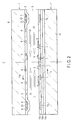
- FIG. 2 is a partial cross-sectional diagram illustrating a second example of the liquid crystal display substrate 1 according to the present embodiment.
- a pixel or a sub-pixel is a minimum unit of the liquid crystal display.
- This FIG. 2 illustrates a vertical cross-section cut along the longitudinal direction of the comb teeth provided to the first through third electrodes 6, 7 and 9.
- At least one layer (two layers in FIG. 2 ) of the insulating layers 10a and 10b is formed above a first surface of the array substrate 4.
- the second electrode 7 is formed at a particular position above the insulating layer 10b.
- At least one layer of the insulating layer 10c is formed above the insulating layer 10b formed on the second electrode 7.
- the first electrode 6 is formed at a particular position above an insulating layer 10c.
- the liquid crystal layer 5 is formed above the insulating layer 10c and the first electrode 6.
- a transparent resin layer 2 is disposed on the liquid crystal layer 5.
- the black matrix 13 having openings and the third electrode 9 provided inside this black matrix are disposed at a particular position above the top surface (reverse side of the liquid crystal layer 5).
- the black matrix 13 is disposed at both ends in the horizontal direction of the cross-section of the pixel shown in FIG. 2 .
- the substrate 8 is disposed above the transparent resin layer 2, the third electrode 9 and the black matrix 13, the substrate 8 is disposed.
- the third electrodes 9 are disposed on the surface on the liquid crystal layer 5 side of the substrate 8 to be symmetrical about the central axis C of the cross-section of the pixel.
- the second electrode 7 is disposed with the insulating layers 10a and 10b interposed therebetween.
- the first electrode 6 is disposed with the insulating layer 10c interposed therebetween.
- the second electrode 7 shown in FIG. 2 includes a section 7a having the same width as that of the black matrix 13 at a position below the black matrix 13 and on the side of the array substrate 4 as viewed in a planar view. In the second electrode 7, by applying a common potential to the section 7a located below the black matrix 13 in a planar view, the crosstalk between adjacent pixels or adjacent sub-pixels can be mitigated.
- the first electrode 6 and the second electrode 7 are symmetrically formed about the central axis C of the cross-section of the pixel in the horizontal direction.
- the comb teeth of the second electrode 7 are shifted from the comb teeth of the first electrode 6 in the second direction 11b.
- the comb teeth of the third electrode 9 are shifted from the comb teeth of the first electrode 6 in the first direction 11a.
- the liquid crystal layer 5 has negative dielectric constant anisotropy, and includes liquid crystal molecules which are vertically aligned in an initial state.
- the vertically-aligned liquid crystal layer 5 is interposed between the counter substrate 3 and the array substrate 4.
- the arrow denoted with D represents a direction of tilt of liquid crystals.
- the axis of the liquid crystal molecules tilts in the first direction 11a at the time of applying a driving voltage, and thus transmission display can be made.
- the axis of the liquid crystal molecules tilts in the second direction 11b at the time of applying the driving voltage, and thus the transmission display can be made.
- FIG. 3 is a perspective view illustrating an exemplary arrangement of the first through third electrodes 6, 7 and 9.
- any comb teeth 7a of the second electrode 7 in the horizontal direction is shifted in the first direction 11a from the position of the comb teeth 6a of the first electrode 6 corresponding to the comb teeth 7a of the second electrode 7 in the horizontal direction.
- any comb teeth 9a of the third electrode 9 in the horizontal direction is shifted in the second direction 11b from the position of the comb teeth 6a of the first electrode 6 corresponding to the comb teeth 9a of the third electrode 9.
- the first direction 11a and the second direction 11b are opposite to each other.
- FIGS. 4 , 5 and 6 illustrate the cross-section of a half of a pixel.
- FIG. 4 is a partial cross-sectional diagram illustrating an example of pixels on the left-hand side from the central axis C under no application of a driving voltage.
- liquid crystal molecules 5a to 5f of the liquid crystal layer 5 are vertically aligned with respect to the respective surfaces (which are positioned above the alignment film (not illustrated)) of the counter substrate 3 and the array substrate 4 when no driving voltage is applied.
- FIG. 5 is a partial cross-sectional diagram illustrating an example of pixels on the left-hand side from the central axis C immediately after the application of the driving voltage.
- electrical flux lines 14a to 14d are formed starting from the first electrode 6 (pixel electrode) toward the third electrode 9 (common electrode). Furthermore, the liquid crystal molecules 5a to 5d begin to tilt to make the axes of the liquid crystal molecules 5a to 5d perpendicular to the directions of the electrical flux lines 14a to 14d.
- electrical flux lines 14e and 14f are formed starting from the first electrode 6 toward the second electrodes 7 (common electrodes). Further, the liquid crystal molecules 5e and 5f begin to tilt to make the axes of the liquid crystal molecules 5e and 5f perpendicular to the directions of the electrical flux lines 14e and 14f.
- FIG. 6 is a partial cross-sectional diagram illustrating an example of pixels on the left-hand side from the central axis C after a lapse of a predetermined time from the application of a driving voltage.
- the inclinations of the liquid crystal molecules 5a to 5d vary depending on the amplitude of the voltage. As illustrated in FIG. 6 , the inclinations of the liquid crystal molecules 5a to 5f each are different according to the distances from the first electrode 6. Furthermore, the pixel is symmetrically formed about the central axis C. Therefore, depending on the inclinations of the liquid crystal molecules and the symmetric structure of the pixel, the liquid crystal molecules may be differently inclined at the time of applying the driving voltage, and thus it is possible to widen a viewing angle of the liquid crystal display.
- FIG. 7 is a partial cross-sectional diagram illustrating an example of a rectangular pixel on the left-hand side.
- FIG. 8 is a partial cross-sectional diagram illustrating an example of a rectangular pixel on the right-hand side.
- the direction of tilts of the liquid crystal molecules 5g to 5j in the liquid crystal layer 5 are settable depending on the directions of shifting the first electrode 6 with respect to the second electrode 7 and the third electrode 9.
- a protruding width W1 in the horizontal direction between the first electrode 6 and the second electrode 7 is appropriately adjusted based on the dimension of the liquid crystal cell, a relation with the driving voltage applied to the liquid crystals, or the like.
- the protruding width W1 may be set to about 0.5 ⁇ m to 6 ⁇ m.
- the protruding width W1 may be reduced less than the thickness of the liquid crystal layer 5 in order to improve responsiveness of the liquid crystals.
- the overlapping width W2 in the horizontal direction between the first electrode 6 and the second electrode 7 is adjusted based on an electric capacitance volume of the liquid crystal cell (pixel or sub-pixel) from the view point of the use of auxiliary capacity.
- the width W3 of the first electrode 6 is appropriately adjusted based on a material used in the liquid crystal layer 5, conditions of the liquid crystal cell, conditions for the driving, and the like.
- the widths of the second and third electrodes 7 and 9 are also adjusted depending on the conditions of the liquid crystal cell.
- the width W3 of the first electrode is adjusted in the range from 2 ⁇ m to 20 ⁇ m in correspondence with the pixel size or the sub-pixel size.
- the distance W4 between the center of the comb teeth of the first electrode 6 and the center of the comb teeth of the third electrode 9, for example, is adjusted based on the conditions of the liquid crystal cell such as the dimension of the liquid crystal cell or the alignment characteristic of the liquid crystals to be used.
- the distance W4, for example is set in the range from 2 ⁇ m to 30 ⁇ m.
- the portion corresponding to the overlapping width W2 between the first electrode 6 and the second electrode 7 may be used as an auxiliary capacitor.
- the protruding width W1 and the overlapping width W2 may be changed in one pixel based on at least one of the formation positions and the number of first electrodes 6 in the liquid crystal cell.
- the liquid crystal molecules of the liquid crystal layer 5 may be driven through the configuration in which plural TFT elements are formed in one pixel and the driving voltage is set to be different in the plural TFT elements.
- the driving voltage to be applied to the first electrode 6, the second electrode 7, or the like may employ an offset (voltage shift). For example, in a case where one pixel or one sub-pixel is driven by two active elements or more and in similar cases, the timing or waveform of an applied voltage of the driving voltage of an active element may be adjusted.
- the offset may be made by causing the amplitude of the voltage to be shifted and also the timing of applying the voltage to be shifted.
- a common voltage to be applied to the second electrode 7 or a common voltage to be applied to the third electrode 9 may be obtained by modulating the common voltage in order to improve responsiveness of the liquid crystals.
- Vertically aligned liquid crystals essentially have an angle of inclination (a pre-tilt angle) of, for example, 89 degrees.
- Vertically aligned liquid crystals in general, tilt in a direction in which the angle of inclination becomes small at the time of applying the driving voltage.
- the direction of tilt of the liquid crystal molecules is set by an initial tilt angle at the time of applying the driving voltage.
- each pixel or each sub-pixel is necessary for the alignment film (not illustrated) to be subjected to a rubbing process in plural directions or to be subjected to a photo-alignment process in plural direction.
- the direction of tilt of the liquid crystal molecules is determined based on the electrical flux lines generated by the oblique electric field without making an inclination angle in the initial alignment of the vertically aligned liquid crystals.
- the initial alignment of the liquid crystals is set to be vertical alignment of substantially 90°. As described above, in the embodiment, there is no need to make the pre-tilt angle for the liquid crystals.
- the pre-tilt angle for example, in the range of about 89.7° to 88° may be formed in the liquid crystals using a PSA method.
- the ultra-high speed responsiveness can be achieved in the liquid crystal display device according to the embodiment.
- the liquid crystals are irradiated with light such as ultraviolet radiation while a driving voltage is applying to the first electrode and the like, so that the pre-tilt angle is formed in the alignment film or the inner wall of the liquid crystal cell. Based on the pre-tilt angle formed in the alignment film or the inner walls of the liquid crystal cell, the liquid crystal molecules are aligned at the pre-tilt angle.
- the initial alignment of the liquid crystals may be a vertical alignment or a horizontal alignment.
- the liquid crystal display device according to the embodiment may be a normally black display type or a normally white display type.
- the liquid crystal display device according to the embodiment may be configured such that the counter substrate including the color filter and the like is disposed to face the array substrate 4 on which the liquid crystal driving element such as the TFT and the like are formed, and the liquid crystal layer 5 is interposed between the counter substrate 3 and the array substrate 4.
- the initial alignment of the liquid crystals is the horizontal alignment, the liquid crystals are risen from the horizontal direction to the vertical direction at the time of applying the voltage.
- the liquid crystal layer 5 may employ either liquid crystals having negative dielectric constant anisotropy type of liquid crystals or liquid crystals having positive dielectric constant anisotropy.
- a nematic liquid crystals may be employed which has a refractive index anisotropy ranging from 0.08 to 0.16 at about room temperature.
- the liquid crystals having a high refractive index anisotropy for example, the liquid crystals having ⁇ n in the range of 0.1 to 0.16, may be employed.
- a liquid crystal material having a wider refractive index anisotropy characteristic may be employed.
- a liquid crystal material hereinafter, referred to as a fluorine liquid crystal
- fluorine liquid crystal containing fluorine atoms in the molecular structure
- the liquid crystal layer 5 is formed thick in some degree for the purpose of a high dielectric constant or a low saturation voltage, since the liquid crystals corresponding to the protruding portion of the second electrode 7 operates in high-speed responsiveness, the driving of liquid crystals at a lower voltage or the high driving speed of liquid crystals can be realized rather than the driving of liquid crystals in the related art.
- the liquid crystal material having low dielectric constant anisotropy has a low viscosity. Using a low viscosity type of liquid crystal material, it is possible to reduce the falling time ( ⁇ decay) when the driving voltage is off.
- the fluorine liquid crystal having a low dielectric constant is rarely mixed with ionic incombustibles; performance degradation such as degradation in a voltage holding rate due to impurities or the burn-in phenomenon of the display is reduced; and display unevenness does not easily occur. It is possible to reduce a threshold voltage or a rising time ( ⁇ rise) using the liquid crystal material having a large absolute value of the dielectric constant anisotropy. In a case where the liquid crystal material having a large absolute value of the dielectric constant anisotropy is used, since the liquid crystals have a low viscosity, for example, a small amount of viscosity reducing agent such as an aluminum compound may be added to the liquid crystals.
- the thickness of the liquid crystal layer 5 is not particularly limited.
- the thickness of the liquid crystal layer 5 may be equal to or less than 3.5 ⁇ m, and preferably a thin layer in the range of 1.5 ⁇ m to 3.4 ⁇ m may be applied in order to realize an ultrahigh-speed responsiveness of the liquid crystal display.
- the oblique electric field is used together with the protruding structure.
- a viscosity, a relative dielectric constant, a birefringence index, an elastic constant of the liquid crystals are optimized, so that the power consumption in the liquid crystal display device can be reduced rather than the related art.
- the parameter An of the liquid crystal layer 5 which is effectively applicable in the embodiment is, for example, in the range of about 200 nm to 500 nm.
- a polyimide organic polymer film or an organic polymer having a polysiloxane structure may be employed by heating the films to be hardened.
- one to three pieces of retardation plates which are sealed to the polarizing plate can be employed.
- FIGS. 9 to 11 examples of plan arrangement states of the first through third electrodes 6, 7 and 9 will be described using FIGS. 9 to 11 .
- FIGS. 9 to 11 for example, the arrangement state of the third electrode 9 in the vertical direction will be exemplified.
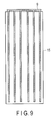
- FIG. 9 is a top plan view illustrating a first example of the third electrode 9.
- the third electrode 9 is provided with respect to the pixel 15 having a rectangular shape in a plan view.
- the third electrode 9 is in the comb-tooth shape.
- the longitudinal direction of the comb teeth of the third electrode 9 is parallel to any sides of the pixel 15 in a plan view.
- the third electrode 9 is provided substantially parallel to the surface on the liquid crystal side of the substrate 8 of the counter substrate 3.
- the second electrode 7 is disposed on the lower side of the first electrode 6 with a gap with respect to the first electrode 6 to be parallelized thereto.
- the third electrode 9 is disposed on the upper side of the first electrode 6 with a gap with respect to the first electrode 6 to be parallelized thereto. This configuration is equally applied to the following descriptions of FIGS. 10 and 11 .
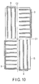
- FIG. 10 is a top plan view illustrating a second example of the third electrode 9.
- the pixel 15 having a rectangular shape in a plan view is divided into four division regions by the center line C1 in the horizontal direction and by the center line C2 in the vertical direction. Further, each of the division regions is provided with the third electrode 9 in the comb-shaped form.
- the longitudinal direction of the comb teeth in the respective third electrodes 9 are parallel to the center line C1, the center line C2, or any sides of the pixel.
- the four third electrodes 9 in the four division regions are disposed so as to be symmetrical about a point.
- the longitudinal direction of the comb teeth of the second electrodes 9 in the division regions of the contact sides may be differently set.
- the four third electrodes 9 may include the electrodes having different longitudinal directions of the comb teeth.
- FIG. 11 is a top plan view illustrating a third example of the third electrode 9.
- the longitudinal direction of the comb teeth of the third electrode 9 is not parallel to the respective sides of the respective pixels or the respective division regions.
- the pixel 15 having the rectangular shape in a plan view is divided into four division regions by the center line C1 in the horizontal direction and by the center line C2 in the vertical direction.
- the two third electrodes 9 are allocated for one pixel 15.
- One of the two third electrodes 9 is disposed on the right side of the pixel 15, and the other one is disposed on the left side of the pixel 15.
- the longitudinal direction of the comb teeth of the two third electrodes 9 are inclined to the center line C1 and the center line C2. In other words, the longitudinal directions of the comb teeth are neither parallel nor perpendicular to the center line C1 in the horizontal direction and the center line C2 in the vertical direction in a plan view.
- the two third electrodes 9 are disposed so as to be symmetrical about a point.
- the pixel 15 is divided into plural regions. Then, the longitudinal directions of the comb teeth in the plural regions are changed, so that it is possible to obtain a wide visibility angle.
- the first electrode 6 and the second electrode 7 may be also disposed in the same state as that of the third electrode 9.
- the second electrode 7 is disposed on the lower side of the first electrode 6 with a gap with respect to the first electrode 6 to be parallelized thereto.
- the third electrode 9 is disposed on the upper side of the first electrode 6 with a gap with respect to the first electrode 6 to be parallelized thereto.
- the comb teeth of the second electrode 7 and the comb teeth of the third electrode 9 are shifted from the first electrode 6 in a direction (horizontal direction) parallel to the substrates 8 and 12 in cross-sectional view perpendicular to the longitudinal direction of the comb teeth.
- the shifting direction from the first electrode 6 to the second electrode 7 in the horizontal direction is opposite to the shifting direction from the first electrode 6 to the third electrode 9 in the horizontal direction.
- the first through third electrodes 6, 7 and 9 described above has been described in connection to the case of the formation in a unit of pixel 15. However, for example, the first through third electrodes 6, 7 and 9 described above may be formed in a unit of sub-pixel.
- planar shape of the pixel or the sub-pixel has been described as the rectangular shape in FIGS. 9 to 11 , but other shapes may be employed.
- a shape such as a parallelogram may be employed which has facing sides are parallel to each other.
- the black matrix 13 is used to increase contrast of the liquid crystal display, which serves as a light blocking pattern disposed in a frame of the pixel or the sub-pixel (smallest unit of display) or at both sides of the pixel.
- the rectangular pixel corresponds to the opening of the black matrix 13, and is synonymous with a "picture element".
- the materials of the first electrode 6 and the second electrode 7 disposed on an array substrate 12 may include a conductive metal oxide such as ITO.
- a metal more conductive than the metal oxide may be employed.
- the liquid crystal display is a reflective type or a transflective (semi-transparent) type
- at least one material of the first electrode 6 and the second electrode 7 may be a thin film made of aluminum or aluminum alloy.
- an aluminum oxide protection layer may be formed on these thin films.
- the first electrode 6, the second electrode 7, and the metal wiring lines of the active elements are formed by interposing at least one of the insulating layers 10a to 10c such as silicon nitride (SiNx) or silicon oxide (SiOx).
- the TFT element and the metal wiring lines connected to the TFT element are not illustrated.
- Japanese Patent Application KOKAI Publication No. 2009-105424 discloses a technology in which gate lines and source lines each are formed using a single aluminum alloy layer having a low contact property for the ITO (conductive metal oxide).
- the liquid crystal display substrate 1 is configured such that the counter substrate 3 is sealed to the array substrate 4 for which an active element such as a TFT is formed.
- the liquid crystal layer 5 is encapsulated between the counter substrate 3 and the array substrate 4.
- the comb-tooth shape or stripe shape of first and second electrodes 6 and 7 are provided. Further, the counter substrate 3 is provided with the comb-tooth shape or stripe shape of third electrode 9.
- the liquid crystal display device according to the embodiment is further provided with a polarizing plate and a retardation plate on both surfaces of the substrate 1.
- the liquid crystal display device according to the embodiment is capable of displaying an image in monochromatic gray scales.
- vertical alignment films may be coated and formed in advance. Further, the alignment films for the vertical alignment are not illustrated in the embodiment.
- there is no need to perform a detailed alignment process for example, an alignment process in which a tilt angle is set to 89°, and plural domains are formed in plural directions
- the tilt angle of the liquid crystals can be set to about 90° through the vertical alignment.
- the liquid crystal molecules of which the initial alignment is the vertical alignment begin to tilt so as to be vertically aligned with respect to the oblique electric field, at the time of applying the driving voltage, under the electrical flux lines (electric fields) generated between the first electrode 6 and the second electrode 7 or under the oblique electric field generated between the first electrode 6 and the third electrode 9.
- the second electrode 7 and the third electrode 9 are shifted in the opposite direction at the first electrode 6.
- the third electrode 9 and the second electrode 7, for example, may be applied with the same potential.
- the first electrode 6 (pixel electrode) may be electrically connected to a drain of the active element (TFT).
- TFT active element
- the TFT and the vertical alignment film are not illustrated.
- disclination can be alleviated, a wide visibility angle can be obtained, and the brightness of the screen can increase.
- an effective driving of liquid crystals can be performed by the oblique electric field, and the liquid crystal can be improved in responsiveness.
- the counter substrate 3 may be configured to include the substrate 8, the third electrode 9 formed above the substrate 8, the black matrix 13 formed above the transparent substrate 8 above which the third electrode 9 is formed, and the transparent resin layer 2 formed above the substrate 3 above which the third electrode 9 and the black matrix 13 are formed.
- the counter substrate 3, for example, may be configured to include the substrate 8, the black matrix 13 formed above the substrate 8, the transparent resin layer 2 formed above the substrate 8 above which the black matrix 13 is formed, and the third electrode 9 which is formed at a position corresponding to the opening of the black matrix 13 above the transparent resin layer 2.
- FIG. 12 is a cross-sectional diagram illustrating an example of a liquid crystal display substrate according to the present embodiment.
- a counter substrate 17 and the array substrate 4 face each other.
- the counter substrate 17 and the array substrate 4 are sealed together, with a liquid crystal layer 5 interposed therebetween.
- the liquid crystal layer 5 is disposed above the top surface of the array substrate 4.
- the third electrode 9 is disposed above the top surface of the liquid crystal layer 5.
- the transparent resin layer 2 is disposed above the top surfaces of the transparent resin layer 2.
- a color filter 18 and the black matrix 13 are disposed above the top surfaces of the transparent resin layer 2.
- the color filter 18 includes, for example, a red filter 18r, a green filter 18g, and a blue filter 18b.
- the substrate 8 is disposed.
- the comb teeth of the third electrode 9 and the comb teeth of the second electrode 7 are provided at the positions overlapping with the black matrix 13.
- FIG. 13 is a cross-sectional diagram illustrating an example of the counter substrate equipped with a color filter.
- the black matrix 13 having openings and the color filter 18 at the openings are formed above top of the color filter 18, the transparent resin layer 2 is formed above top of the color filter 18, the transparent resin layer 2 is formed above top of the transparent resin layer 2, the third electrode 9 is formed.
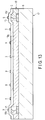
- FIG. 14 is a partial cross-sectional diagram illustrating an example of a pixel immediately after the application of a driving voltage.
- Liquid crystals 5k to 5p of the vertically oriented liquid crystal layer 5 are oriented vertically to the respective surfaces (above an alignment film that is not depicted in the diagram) of the counter substrate 17 and the array substrate 4, under no application of a driving voltage.
- electrical flux lines 14k to 14p that are directed from the first electrode 6, which is a pixel electrode, toward the third electrode 9 are formed, and the liquid crystals 5k to 5p start to tilt such that the axis of the liquid crystals 5k to 5p is perpendicular to the direction of these electrical flux lines 14k to 14p.
- FIG. 15 is a partial cross-sectional diagram illustrating an example of a pixel after a lapse of a predetermined time from the application of a driving voltage.
- the change in the inclination of the liquid crystals 5k to 5p stops depending on the size of the voltage. As shown in FIG. 15 , the liquid crystals 5k to 5p respectively have different inclinations in accordance with the distance from the first electrode 6. Depending on the voltage applied to the first through third electrodes 6, 7 and 9, the liquid crystals 5k to 5p can be made to have different inclinations at the time of the application of a driving voltage, and the field of vision of the liquid crystal display can be extended.
- the counter substrate 17 may include, for example, a light shielding layer as a material for forming the black matrix 13. Also, the counter substrate 17 may include, for example, a color layer as a material for forming the black matrix 13 or a material for forming the color filter 18.
- a light shielding layer is a coating film having light shielding properties, in which a light-shielding pigment is dispersed in a transparent resin. The light shielding layer is generally imparted with photosensitivity. The light shielding layer has a pattern formed therein by a photolithographic technique including exposure and development.
- a color layer is a coating film in which an organic pigment that will be described below is dispersed in a transparent resin. The color layer is formed by forming a coating film at the openings of the black matrix, and forming a pattern according to a photolithographic method.
- the relative permittivity of the color layer is a relatively important characteristic.
- the relative permittivity of this color layer is almost definitively determined based on the ratio of the organic pigment that is added as a colorant with respect to the transparent resin. Therefore, it is difficult to change the relative permittivity to a large extent.
- the kind or content of the organic pigment in the color layer is set based on the color purity required as the liquid crystal display device, and thereby, the relative permittivity of the color layer is also almost determined.
- the relative permittivity can be adjusted to 4 or greater by increasing the ratio of the organic pigment and thereby making the color layer into a thin film.
- the relative permittivity can be slightly increased by using a material having a high refractive index as the transparent resin.
- the relative permittivity of a color layer that uses an organic pigment falls approximately in the range of 2.9 to 4.5.
- a color pixel filter that is included in the color filter 18 may include three colors of a red filter 18r, a green filter 18g, and a blue filter 18b; may also include complementary color-based filters such as a yellow filter; or may also include white pixels (transparent pixels).
- the color filter 18 may be provided not on the side of the counter substrate 17, but on the array substrate 4.
- the liquid crystal display device according to the present embodiment may also be a color liquid crystal display device which is equipped with a LED backlight and utilizes time sharing light emission (field sequential).
- FIG. 16 is a plan view illustrating an example of the shape and arrangement of the top plan view of a pixel including three sub-pixels.
- a rectangular (or square) pixel 19 includes a rectangular red sub-pixel 19r, a rectangular green sub-pixel 19g, and a rectangular blue sub-pixel 19b.
- FIG. 17 is a plan view illustrating an example of the shape and arrangement of the top plan view of a pixel 19 including plural sub-pixels 19r, 19g and 19b, each having a polygonal shape in which the opposite sides are parallel to each other.
- FIG. 17 a color filter in a lateral stripe arrangement is illustrated.
- the lines in the longitudinal direction are corrugated.
- Nine parallelogram-shaped red sub-pixels 19r are arranged in the row direction (transverse direction).
- nine parallelogram-shaped green sub-pixels 19g are arranged in the row direction.
- nine parallelogram-shaped blue sub-pixels 19g are arranged in the row direction.
- the pixel 19 is configured to include nine red sub-pixels 19r, nine green sub-pixels 19g, and nine blue sub-pixels 19b.
- the inclinations of the four sides between the adjoining upper and lower rows are different. That is, two parallelogram-shaped sub-pixels arranged up and down are symmetric about the tangent line and are arranged in a " ⁇ " shape (or an arrowhead shape, a form obtained by rotating the letter "V" by 90°).
- a red sub-pixel 19r and a red sub-pixel 19r that is two rows below across a green sub-pixel 19g and a blue sub-pixel 19b have different angles of the four sides.
- a green sub-pixel 19g and a green sub-pixel 19g that is two rows below across a blue sub-pixel 19b and a red sub-pixel 19r have different angles of the four sides.
- a blue sub-pixel 19b and a blue sub-pixel 19b that is two rows below across a red sub-pixel 19r and a green sub-pixel 19g have different angles of the four sides.
- FIG. 18 is a plan view illustrating an example of the shape and arrangement of the top plan view of a pixel 19 in a longitudinal stripe arrangement, which includes plural parallelogram-shaped sub-pixels 19r, 19g and 19b.
- the lines in the longitudinal direction are corrugated.
- a red sub-pixel 19r, a green sub-pixel 19g, and a blue sub-pixel 19b are arranged in the row direction, and plural red sub-pixels 19r, plural green sub-pixels 19g, and plural blue sub-pixels 19b are respectively arranged in the column direction (longitudinal direction).
- FIG. 19 is a plan view illustrating an example of the shape and arrangement of the top plan view of a pixel 19 in a lateral stripe arrangement, which includes plural parallelogram-shaped sub-pixels 19r, 19g and 19b.
- the comb teeth directions of the first through third electrodes 6, 7 and 9 may be parallel to the upper side or the lower side, or may be parallel to the oblique side.
- plural red sub-pixels 19r, plural green sub-pixels 19g, and plural blue sub-pixels 19b are respectively arranged in the row direction, and a red sub-pixels 19r, a green sub-pixel 19g and a blue sub-pixel 19b are arranged in the longitudinal direction.
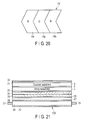
- FIG. 20 is a plan view illustrating an example of the shape and arrangement of the top plan view of the sub-pixels 19r, 19g and 19b, and the pixel 19, in which the " ⁇ " shape is formed in a unit.
- the pixel 19 may be constructed by the sub-pixels 19r, 19g and 19b having the " ⁇ " shape.
- Plural pixels 19 may be in a lateral stripe arrangement, or may be in a longitudinal stripe arrangement.
- the comb teeth direction of the first through third electrodes 6, 7 and 9 can be arranged in parallel to any side of the pixel or sub-pixel.
- disclination can be reduced, the viewing angle can be widened, and the screen can be made brighter.
- liquid crystal driving can be effectively carried out by an oblique electric field, and the responsiveness of liquid crystals can be enhanced.
- the shape of the pixel 19 and the sub-pixels 19r, 19g and 19b can be freely set, and thereby, the alignment of the liquid crystals can be changed, while a wide viewing angle can be realized.
- the counter substrate 17 may be configured to include a substrate 8, a third electrode 9 formed above the substrate 8, the black matrix 13 formed above the substrate 8 above which the third electrode 9 is formed, the color filter 18 formed at the openings of the black matrix 13, and the transparent resin layer 2 formed above the color filter 18.
- the counter substrate 17 may also be configured to include, for example, the substrate 8, the black matrix 13 formed above the substrate 8, the third electrode 9 formed at the openings of the black matrix 13, the color filter 18 formed at the openings of the black matrix 13 above which the third electrode 9 is formed, and the transparent resin layer 2 formed above the color filter 18.
- a photosensitive color composition used in the formation of a light shielding layer or a color layer contains a pigment dispersion, as well as a polyfunctional monomer, a photosensitive resin or a non-photosensitive resin, a polymerization initiator, a solvent and the like.
- highly transparent organic resins that can be used in the present embodiment such as photosensitive resins and non-photosensitive resins, are collectively referred to as transparent resins.
- Transparent resins include thermoplastic resins, thermosetting resins, or photosensitive resins.
- thermoplastic resins include a butyral resin, a styrene-maleic acid copolymer, chlorinated polyethylene, chlorinated polypropylene, polyvinyl chloride, a vinyl chloride-vinyl acetate copolymer, polyvinyl acetate, a polyurethane-based resin, a polyester resin, an acrylic acid resin, an alkyd resin, a polystyrene resin, a polyamide resin, a rubber-based resin, a cyclized rubber-based resin, a cellulose, polybutadiene, polyethylene, polypropylene, and a polyimide resin.
- thermosetting resins examples include an epoxy resin, a benzoguanamine resin, a rosin-modified maleic acid resin, a rosin-modified fumaric acid resin, a melamine resin, a urea resin, and a phenolic resin.
- thermosetting resin for example, a substance obtainable by causing a melamine resin to react with a compound containing an isocyanate group may also be used.
- the transparent resin is preferably a resin imparted with alkali-solubility.
- the alkali-soluble resin a resin containing a carboxyl group or a hydroxyl group can be used.
- the alkali-soluble resin that can be used include an epoxy acrylate-based resin, a novolac-based resin, a polyvinylphenol-based resin, an acrylic resin, a carboxyl group-containing epoxy resin, and a carboxyl group-containing urethane resin.
- Preferred examples of the alkali-soluble resin include an epoxy acrylate-based resin, a novolac-based resin, and an acrylic resin, and particularly preferred examples include an epoxy acrylate-based resin and a novolac-based resin.
- the transparent resin for example, the following acrylic resins can be applied.
- acrylic resin use is made of polymers obtainable by using, as monomers, for example, (meth)acrylic acid; alkyl (meth)acrylates such as methyl (meth)acrylate, ethyl (meth)acrylate, propyl (meth)acrylate, butyl (meth)acrylate, t-butyl (meth)acrylate, pentyl (meth)acrylate, and lauryl (meth)acrylate; hydroxyl group-containing (meth)acrylates such as hydroxyethyl (meth)acrylate and hydroxypropyl (meth)acrylate; ether group-containing (meth)acrylates such as ethoxyethyl (meth)acrylate and glycidyl (meth)acrylate; and alicyclic (meth)acrylates such as cyclohexyl (meth)acrylate, isobornyl (meth)acrylate, and dicyclopentenyl (meth)acrylate.
- one kind of substance may be used, or two or more kinds of substances may be used in combination.
- copolymers of compounds capable of copolymerizing with the monomers such as styrene, cyclohexyl maleimide or phenylmaleimide, may also be used as the acrylic resin.
- a resin having photosensitivity may also be obtained by causing a copolymer obtained by copolymerizing carboxylic acid having an ethylenically unsaturated group, such as (meth)acrylic acid, to react with a compound containing an epoxy group and an unsaturated double bond, such as glycidyl methacrylate.
- carboxylic acid having an ethylenically unsaturated group such as (meth)acrylic acid
- a resin having photosensitivity may also be obtained by adding a carboxylic acid-containing compound such as (meth)acrylic acid, to a copolymer of a polymer of epoxy group-containing (meth)acrylate such as glycidyl methacrylate or a polymer of epoxy group-containing (meth)acrylate such as glycidyl methacrylate, with another (meth)acrylate.
- a carboxylic acid-containing compound such as (meth)acrylic acid
- a copolymer of a polymer of epoxy group-containing (meth)acrylate such as glycidyl methacrylate
- a polymer of epoxy group-containing (meth)acrylate such as glycidyl methacrylate
- a resin having photosensitivity may also be obtained by causing a polymer having a hydroxyl group and a monomer such as hydroxyethyl methacrylate, to react with a compound having an isocyanate group and an ethylenically unsaturated group, such as methacryloyloxyethyl isocyanate.
- a resin having a carboxyl group can be obtained by causing a copolymer of hydroxyethyl methacrylate having plural hydroxyl groups or the like to react with a polybasic acid anhydride, and introducing a carboxyl group to the copolymer.
- the method for producing a resin having a carboxyl group is not intended to be limited to this method only.
- Examples of the acid anhydride used in the reaction described above include, for example, malonic anhydride, succinic anhydride, maleic anhydride, itaconic anhydride, phthalic anhydride, tetrahydrophthalic anhydride, hexahydrophthalic anhydride, methyltetrahydrophthalic anhydride, and trimellitic anhydride.
- the solid component acid value of the acrylic resin described above is preferably 20 mg KOH/g to 180 mg KOH/g. If the acid value is smaller than 20 mg KOH/g, the rate of development of the photosensitive resin composition is too slow, and a longer time is required for development, so that productivity tends to deteriorate. Furthermore, if the solid component acid value is larger than 180 mg KOH/g, on the contrary, the rate of development is too fast, defects such as pattern peeling or pattern chipping after development tend to occur.
- the double bond equivalent of this acrylic resin is preferably 100 or greater, more preferably 100 to 2000, and most preferably 100 to 1000. If the double bond equivalent is greater than 2000, sufficient photocurability may not be obtained.
- photopolymerizable monomer examples include various acrylic acid esters and methacrylic acid esters, such as 2-hydroxyethyl (meth)acrylate, 2-hydroxypropyl (meth)acrylate, cyclohexyl (meth)acrylate, polyethylene glycol di(meth)acrylate, pentaerythritol tri(meth)acrylate, trimethylolpropane tri(meth)acrylate, dipentaerythritol hexa(meth)acrylate, tricyclodecanyl (meth)acrylate, melamine (meth)acrylate, and epoxy (meth)acrylate; (meth)acrylic acid, styrene, vinyl acetate, (meth0acrylamide, N-hydroxymethyl (meth)acrylamide, and acrylonitrile.
- acrylic acid esters and methacrylic acid esters such as 2-hydroxyethyl (meth)acrylate, 2-hydroxypropyl (meth)acrylate, cyclohexy
- a polyfunctional urethane acrylate having a (meth)acryloyl group that is obtainable by causing a (meth)acrylate having a hydroxyl group to react with a polyfunctional isocyanate is preferably used.
- the combination of the (meth)acrylate having a hydroxyl group and the polyfunctional isocyanate is arbitrary and is not particularly limited.
- one kind of a polyfunctional urethane acrylate may be used alone as the photopolymerizable monomer, or two or more kinds can also be used in combination.
- photopolymerization initiator examples include acetophenone-based compounds such as 4-phenoxydichloroacetophenone, 4-t-butyldichloroacetophenone, diethoxyacetophenone, 1-(4-isopropylphenyl)-2-hydroxy-2-methylpropan-1-one, 1-hydroxycyclohexyl phenyl ketone, and 2-benzyl-2-dimethylamino-1-(4-morpholiniophenyl)-butan-1-one; benzoin-based compounds such as benzoin, benzoin methyl ether, benzoin ethyl ether, benzoin isopropyl ether, and benzyl dimethyl ketal; benzophenone-based compounds such as benzophenone, benzoylbenzoic acid, methyl benzoylbenzoate, 4-phenylbenzophenone, hydroxybenzophenone, acrylated benzophenone, and 4-benzoyl-4'-methyldip
- the sensitizer for example, it is preferable to use a photopolymerization initiator and a sensitizer in combination.
- the sensitizer that can be used in combination include compounds such as a-acyloxy ester, acylphosphine oxide, methylphenyl glyoxylate, benzyl-9,10-phenanthrenequinone, camphor-quinone, ethylanthraquinone, 4,4'-diethylisophthalophenone, 3,3',4,4'-tetra(t-butylperoxycarbonyl)benzophenone, and 4,4'-diethylaminobenzophenone.
- the sensitizer can be incorporated in an amount of from 0.1 parts by mass to 60 parts by mass, relative to 100 parts by mass of the photopolymerization initiator.
- the photopolymerization initiators described above are preferably used together with ethylenically unsaturated compounds.
- An ethylenically unsaturated compound means a compound having one or more ethylenically unsaturated bonds in the molecule.
- the photopolymerization initiator is preferably a compound having two or more ethylenically unsaturated bonds in the molecule, from the viewpoint of enhancing polymerizability, crosslinkability, and the difference in the solubility in the developing solution between exposed areas and non-exposed areas associated therewith.
- the photopolymerization initiator is particularly preferably a (meth)acrylate compound in which the unsaturated bond is derived from a (meth)acryloyloxy group.
- Examples of the compound having one or more ethylenically unsaturated bonds in the molecule that may be used include unsaturated carboxylic acids such as (meth)acrylic acid, crotonic acid, isocrotonic acid, maleic acid, itaconic acid and citraconic acid, and alkyl esters thereof; (meth)acrylonitrile; (meth)acrylamide; and styrene.
- unsaturated carboxylic acids such as (meth)acrylic acid, crotonic acid, isocrotonic acid, maleic acid, itaconic acid and citraconic acid, and alkyl esters thereof; (meth)acrylonitrile; (meth)acrylamide; and styrene.
- Examples of the compound having two or more ethylenically unsaturated bonds in the molecule that may be used include esters between unsaturated carboxylic acids and polyhydroxy compounds; (meth)acryloyloxy group-containing phosphates; urethane (meth)acrylates between hydroxy(meth)acrylate compounds and polyisocyanate compounds; and epoxy (meth)acrylates between (meth)acrylic acid or hydroxy(meth)acrylate compounds and polyepoxy compounds.
- the photopolymerizable initiator, sensitizer and ethylenically unsaturated compounds described above may be added to a composition containing a polymerizable liquid crystal compound, in the case of forming a retardation layer inside a liquid crystal cell.
- a polyfunctional thiol that functions as a chain transfer agent can be incorporated.
- the polyfunctional thiol may be a compound having two or more thiol groups, and examples thereof that can be used include hexanedithiol, decanedithiol, 1,4-butanediol bisthiopropionate, 1,4-butanediol bisthioglycolate, ethylene glycol bisthioglycolate, ethylene glycol bisthiopropionate, trimethylolpropane tristhioglycolate, trimethylolpropane tristhiopropionate, trimethylolpropanetris(3-mercaptobutyrate), pentaerythritol tetrakisthioglycolate, pentaerythritol tetrakisthiopropionate, trimercaptopropionic acid tris(2-hydroxyethyl)isocyanurate, 1,4-d
- polyfunctional thiols can be used singly or as mixtures of two or more kinds.
- the polyfunctional thiol can be used in an amount of preferably 0.2 parts to 150 parts by mass, and more preferably 0.2 parts to 100 parts by mass, relative to 100 parts by mass of the pigment in the photosensitive coloring composition.
- a storage stabilizer can be incorporated in order to stabilize the viscosity over time of the composition.
- the storage stabilizer that can be used include quaternary ammonium chlorides such as benzyl trimethyl chloride and diethylhydroxyamine; organic acids such as lactic acid and oxalic acid, and methyl ethers thereof; organic phosphines such as t-butylpyrocatechol, triethylphosphine, and triphenylphosphine; and phosphorous acid salts.
- the storage stabilizer can be incorporated in an amount of from 0.1 parts by mass to 10 parts by mass relative to 100 parts by mass of the pigment in the photosensitive coloring composition.
- an adhesion improving agent such as a silane coupling agent can be incorporated in order to increase the adhesiveness to the substrate.
- the silane coupling agent that can be used include vinyl silanes such as vinyl tris( ⁇ -methoxyethoxy)silane, vinyl ethoxysilane, and vinyl trimethoxysilane; (meth)acrylsilanes such as ⁇ -methacryloxypropyl trimethoxysilane; epoxysilanes such as ⁇ -(3,4-epoxycyclohexyl)ethyl trimethoxysilane, ⁇ -(3,4-epoxycyclohexyl)methyl trimethoxysilane, ⁇ -(3,4-epoxycyclohexyl)ethyl triethoxysilane, ⁇ -(3,4-epoxycyclohexyl)methyl triethoxysilane, ⁇ -glycidoxypropyl trimethoxysilane
- a solvent such as water or an organic solvent is incorporated.
- the composition used in the present embodiment forms a color layer of a color filter, the solvent also has a function of uniformly dispersing the pigment.
- Examples of the solvent that can be used include cyclohexanone, ethylcellosolve acetate, butylcellosolve acetate, 1-methoxy-2-propyl acetate, diethylene glycol dimethyl ether, ethylbenzene, ethylene glycol diethyl ether, xylene, etylcellosolve, methyl n-amyl ketone, propylene glycol monomethyl ether, toluene, methyl ethyl ketone, ethyl acetate, methanol, ethanol, isopropyl alcohol, butanol, isobutyl ketone, and petroleum-based solvents.
- the solvent can be incorporated in an amount of from 800 parts by mass to 4000 parts by mass, and preferably from 1000 parts by mass to 2500 parts by mass, relative to 100 parts by mass of the pigment in the coloring composition.
- red pigments examples include C.I. Pigment Red 7, 9, 14, 41, 48:1, 48:2, 48:3, 48:4, 81:1, 81:2, 81:3, 97, 122, 123, 146, 149, 168, 177, 178, 179, 180, 184, 185, 187, 192, 200, 202, 208, 210, 215, 216, 217, 220, 223, 224, 226, 227, 228, 240, 242, 246, 254, 255, 264, 272, and 279.
- yellow pigments examples include C.I. Pigment Yellow 1, 2, 3, 4, 5, 6, 10, 12, 13, 14, 15, 16, 17, 18, 20, 24, 31, 32, 34, 35, 35:1, 36, 36:1, 37, 37:1, 40, 42, 43, 53, 55, 60, 61, 62, 63, 65, 73, 74, 77, 81, 83, 86, 93, 94, 95, 97, 98, 100, 101, 104, 106, 108, 109, 110, 113, 114, 115, 116, 117, 118, 119, 120, 123, 125, 126, 127, 128, 129, 137, 138, 139, 144, 146, 147, 148, 150, 151, 152, 153, 154, 155, 156, 161, 162, 164, 166, 167, 168, 169, 170, 171, 172, 173, 174, 175, 176, 177, 179, 180, 181, 18
- blue pigments examples include C.I. Pigment Blue 15, 15:1, 15:2, 15:3, 15:4, 15:6, 16, 22, 60, 64, and 80.
- C.I. Pigment Blue 15:6 is preferred.
- violet pigments examples include C.I. Pigment Violet 1, 19, 23, 27, 29, 30, 32, 37, 40, 42, and 50. Among these, C.I. Pigment Violet 23 is preferred.
- green pigments examples include C.I. Pigment Green 1, 2, 4, 7, 8, 10, 13, 14, 15, 17, 18, 19, 26, 36, 45, 48, 50, 51, 54, 55, and 58.
- C.I. Pigment Green 58 is preferred.
- the pigment kinds of C.I. Pigments may be described simply with abbreviations such as PB (Pigment Blue), PV (Pigment Violet), PR (Pigment Red), PY (Pigment Yellow), and PG (Pigment Green).
- a light shielding coloring material that is included in the light shielding layer or black matrix is a coloring material exhibiting a light shielding function by having absorption in the visible light wavelength region.
- the light shielding coloring material for example, an organic pigment, an inorganic pigment, a dye, and the like are used.
- the inorganic pigment that may be used include carbon black and titanium oxide.
- the dye that may be used include azo-based dyes, anthraquinone-based dyes, phthalocyanine-based dyes, quinoneimine-based dyes, quinoline-based dyes, nitro-based dyes, carbonyl-based dyes, and methine-based dyes.
- the organic pigments described above can be employed.
- the light shielding component may be used singly, or two or more kinds may be used together at any combination and proportions.
- these coloring materials may also be imparted with high volume resistivity by coating the surface of the coloring materials with a resin.
- these coloring materials may also be imparted with low volume resistivity, by increasing the content ratio of the coloring material with respect to the parent material of the resin and imparting slight electrical conductivity to the component.
- the volume resistivity value of these light shielding materials is appropriately in the range of 1 ⁇ 10 8 ⁇ cm to 1 ⁇ 10 15 ⁇ cm, which is not at a level capable of affecting the resistance value of the transparent conductive film.
- the relative permittivity of the light shielding layer can also be adjusted approximately in the range of 3 to 11, by means of the selection of the coloring material or the content ratio.
- the relative permittivities of the light shielding layer, the first transparent resin layer, and the coloring layer can be adjusted according to the design conditions for the liquid crystal display device or the driving conditions for the liquid crystals.
- polymer dispersant As the pigment dispersant, it is preferable to use a polymer dispersant as the pigment dispersant, because polymer dispersants have excellent dispersion stability over time.
- the polymer dispersant that can be used include a urethane-based dispersant, a polyethyleneimine-based dispersant, a polyoxyethylene alkyl ether-based dispersant, a polyoxyethylene glycol diester-based dispersant, a sorbitan aliphatic ester-based dispersant, and an aliphatic-modified polyester-based dispersant.
- dispersants formed from graft copolymers containing nitrogen atoms are preferred because those dispersants have excellent developing properties with regard to the light shielding photosensitive resin composition used in the present embodiment, which contains a large proportion of pigments.
- the dispersants may be used singly, or two or more kinds may be used together at any combination and proportions.
- Examples of a dispersion aid that can be used include colorant derivatives.
- Examples of the colorant derivatives that can be used include azo-based, phthalocyanine-based, quinacridone-based, benzimidazolone-based, quinophthalone-based, isoindolinone-based, dioxazine-based, anthraquinone-based, indanthrene-based, perylene-based, perinone-based, diketopyrrolopyrrole-based, and dioxazine-based derivatives.
- quinophthalone-based derivatives are preferred.
- substituents for the colorant derivatives for example, a sulfonic acid group, a sulfonamide group and quaternary salts thereof, a phthalimidomethyl group, a dialkylaminoalkyl group, a hydroxyl group, a carboxyl group, and an amide group may be bonded to the pigment skeleton directly or via an alkyl group, an aryl group, a heterocyclic group or the like.
- a sulfonic acid group is preferably used.
- these substituents may be substituted plural times in a pigment skeleton.
- colorant derivatives examples include sulfonic acid derivatives of phthalocyanine, sulfonic acid derivatives of quinophthalone, sulfonic acid derivatives of anthraquinone, sulfonic acid derivatives of quinacridone, sulfonic acid derivatives of diketopyrrolopyrrole, and sulfonic acid derivatives of dioxazine.
- the dispersion aids and colorant derivatives described above may be used singly, or two or more kinds may be used together at any combination and proportions.
- a black matrix 13 is formed on a transparent substrate 8 which is an alkali-free glass plate.
- a film of ITO (a metal oxide thin film of indium and tin) for forming a third electrode is formed on the transparent substrate 8 on which the black matrix 13 is formed, so as to cover the entire surface, by using a sputtering apparatus.
- This film of ITO is formed to have a film thickness of 0.14 ⁇ m at normal temperature by using a sputtering apparatus.
- ITO is formed in, for example, a comb teeth shape having a width of 7 ⁇ m by a photolithographic method.
- This comb-shaped ITO serves as the third electrode 9, which is a common electrode.
- annealing is required in order to increase the transmittance.
- a heat treatment for annealing may be carried out together with a film curing treatment for the black matrix or the like in the subsequent processes.
- the transparent resin layer 2 is formed on the surface where the third electrode 9 is formed.
- the black matrix 13 and the transparent resin layer 2 are formed by, for example, a forming means that will be described below.
- the pattern width of the third electrode 9 formed from ITO is adjusted to the range of 2 ⁇ m to 30 ⁇ m according to the pixel size.
- the formation density or pattern width of the third electrode 9 may vary within a pixel.
- first and second electrodes 6 and 7 can also be produced by the same technique as that for this third electrode 9.
- a carbon black dispersion liquid is prepared by mixing 20 pats by weight of a carbon pigment, 8.3 parts by weight of a polymer dispersant, 1.0 parts by weight of a copper phthalocyanine derivative (manufactured by Toyo Ink Co., Ltd.), and 71 parts by weight of propylene glycol monomethyl ether acetate, and stirring the mixture with a bead mill dispersing machine.
- a carbon black dispersion liquid for example, a carbon black dispersion liquid, a resin (solids content: 56.1 wt%), a monomer, an initiator, a solvent (propylene glycol monomethyl ether acetate or ethyl 3-ethoxypropionate), and a leveling agent are used. These materials are mixed and stirred at the following composition ratio, and the mixture is used in the resist for forming a black matrix (pigment concentration in the solids content: about 20%).
- the photoresist is spin coated on the transparent substrate 8 which is a glass plate, and the photoresist is dried, for example, at 100°C for 3 minutes.
- a coating film having a film thickness of 1.9 ⁇ m is formed on the surface of the transparent substrate 8.
- the coating film on the transparent substrate 8 is irradiated with light from a light source by using a photomask for exposure having a predetermined pattern width (corresponding to the streak width of the black matrix 13) and an opening pattern.
- the light is irradiated, for example, at a dose of 200 mJ/cm 2 by using an ultrahigh pressure mercury lamp.
- the substrate after light irradiation was subjected to development, for example, for 60 seconds by using a 2.5% aqueous solution of sodium carbonate, and was washed with water and dried.
- the substrate was heat treated at 230°C to 60 minutes, and thus the pattern is fixed.
- a black matrix 13 is formed on the transparent substrate 8.
- the streak width of the black matrix 13 for example, a width of about 20 ⁇ m or about 20.5 ⁇ m is used.
- the black matrix 13 is formed around the pixels or sub-pixels.
- the angle of inclination from the surface of the transparent substrate 8 to the streak end which is the pattern edge is set to about 45°.
- a transparent resin layer 2 is formed so as to cover the black matrix 13 and the openings where there is no black matrix 13, by using an alkali-soluble acrylic photosensitive resin coating liquid.
- the transparent resin layer 2 is formed such that the film thickness after film curing is, for example, about 1 ⁇ m.
- a counter substrate 3 for liquid crystal display is formed.
- the substrate 3 of the present embodiment can be applied to a liquid crystal display device in which a color filter 18 is formed on the side of the array substrate 4, or a field sequential color liquid crystal display device (a technique of performing color display without a color filter by time sharing light source driving by using an LED light source of plural colors as the backlight).
- acrylic photosensitive resin coating liquid for example, a transparent resin coating liquid obtainable by synthesizing an acrylic resin, adding a monomer and a photoinitiator, and performing filtration through a pore size of, for example, 0.5 ⁇ m, can be used.
- Heating is sufficiently carried out after the dropwise addition, and thereafter, a material obtained by dissolving 2.0 parts of the thermal polymerization initiator in 50 parts of cyclohexanone is added to this mixture. The reaction is further continued, and thereby a solution of an acrylic resin is obtained.
- cyclohexanone is added such that the solids content is 30% by weight to prepare an acrylic resin solution, and thus, a resin solution (1) is obtained.
- the weight average molecular weight of the acrylic resin was about 20,000.
- a mixture of the composition described below is uniformly stirred and mixed, and then is dispersed for a predetermined time (2 hours) with a sand mill by using, for example, glass beads having a diameter of 1 mm. Subsequently, the dispersion is filtered through a filter having a pore size of 0.5 ⁇ m, and thus a transparent resin coating liquid is obtained.
- a black matrix 13 is formed on a transparent substrate 8 which is an alkali-free glass plate, in the same pattern by using the photoresist for forming a black matrix described above.
- the following materials are used as the organic pigments to be dispersed in the color layer.
- Dispersion liquids of the respective colors of red, green and blue are prepared by using the pigments described above.
- a mixture of the composition described above is uniformly stirred, and then the mixture is dispersed for a predetermined time (for example, 5 hours) with a sand mill by using glass beads.
- the dispersion is filtered through a filter (for example, a 5- ⁇ m filter), and thus a red pigment dispersion liquid is prepared.
- a green pigment dispersion liquid can be prepared with a mixture of the composition described above by using the same preparation method as that used for the red pigment dispersion liquid.
- a blue pigment dispersion liquid can be prepared with a mixture of the composition described above, by using the same preparation method as that used for the red pigment dispersion liquid.
- a mixture of the composition described above is uniformly stirred and mixed, and then is filtered through a filter having a pore size of 5 ⁇ m. Thereby, a red pixel-forming color resist is obtained.
- a mixture of the composition described above is uniformly stirred and mixed, and then is filtered through a filter having a pore size of 5 ⁇ m. Thereby, a green pixel-forming color resist is obtained.
- the blue pixel-forming color resist is prepared by the same method as for the red pixel-forming color resist such that the composition would be the composition described below.
- a green pigment for example, in a molten salt at 200°C of 356 parts of aluminum chloride and 6 parts of sodium chloride, 46 parts of zinc phthalocyanine is dissolved, and the solution is cooled to 130°C and stirred for one hour. Furthermore, the reaction temperature is increased to 180°C, and bromine is added dropwise thereto at a rate of 10 parts per hour for 10 hours. Thereafter, chlorine is introduced thereto at a rate of 0.8 parts per hour for 5 hours.
- the reaction liquid thus obtained is slowly injected into 3200 parts of water, and then the mixture is filtered and washed with water.
- 107.8 parts of a crude halogenated zinc phthalocyanine pigment is obtained.
- the average number of bromine atoms contained in a molecule of the crude halogenated zinc phthalocyanine pigment is 14.1, while the average number of chlorine atoms is 1.9.
- the mixture obtainable in this manner is introduced into 5000 parts of warm water, and the mixture is stirred for about one hour with a high speed mixer while heated to about 70°C to be in a slurry form. Furthermore, the mixture in a slurry form is repeatedly subjected to filtration and water-washing, and thus the table salt and the solvent are removed. Thereafter, the mixture is dried for 24 hours at 80°C. Thereby, 117 parts of a salt milling-treated green pigment is obtained.
- a color layer is formed by using the color pixel-forming color resist obtained according to the method described above.
- the various conditions for the formation of the color layer as described below merely constitute an example, and other conditions may also be applied.
- a color resist for forming a red pixel-forming color resist is applied on a glass substrate by spin coating such that the finished film thickness is 1.8 ⁇ m.
- the color resist is dried at 90°C for 5 minutes, and then is irradiated with light from a high pressure mercury lamp at a dose of 300 mJ/cm 2 through a photomask for forming color pixels.
- the color resist is developed with an alkali developing solution for 60 seconds, and thus a red color pixel in a stripe form is obtained.
- the red filter 18r red color pixel
- the pixel is produced such that the overlap between the BM areas and color areas is, for example, 8.0 ⁇ m.
- the green pixel-forming resist is also applied similarly by spin coating such that the finished film thickness is 1.8 ⁇ m. After the resist is dried at 90°C for 5 minutes, the resist is subjected to exposure and development through a photomask such that a pattern is formed at a position adjacent to the red pixels described above. Thereby, a green filter 18g (green pixels) is obtained.
- a blue pixel-forming resist is also completed by the same technique as that used for the red and green resists, and a blue filter 18b that is adjacent to the red filter 18r and the green filter 18g is obtained at a film thickness of 1.8 ⁇ m. Thereby, a color filter having coloration of three colors, namely, red, green and blue, on the substrate 8 is obtained. Thereafter, the color filter is cured at 230°C for 30 minutes.
- a transparent resin layer 2 having a film thickness after being cured of 1 ⁇ m is formed so as to cover the entirety of the color filter 18 of three colors, namely, red, green and blue, by using the acrylic photosensitive resin coating liquids.
- the transparent resin layer 2 is subjected to exposure and development, and then is cured at 230°C for 30 minutes.
- an ITO a metal oxide thin film of indium and tin
- a film thickness of 0.14 ⁇ m at room temperature so as to cover the entire surface after the black matrix 13 is formed, by using a sputtering apparatus.
- An ITO film is formed into a comb-shaped third electrode 9 having a width of the common electrode of 7 ⁇ m, by using a known photolithographic method.
- the third electrode 9 is heat treated at 230°C for 30 minutes for annealing of the ITO film, after the pattern formation. Thereby, the counter substrate 17 is formed.
- the third electrode 9 may be formed directly above the transparent substrate 8 such as a glass plate, or may also be formed between the color filter 18 and the transparent resin layer 2.
- FIG. 21 is a cross-sectional diagram illustrating an example of the configuration of the liquid crystal display device according to the present embodiment.
- FIG. 21 an example of the case where a liquid crystal display device 100 includes the substrate 1 is illustrated, but the same also applies to the case of including the substrate 16.
- the liquid crystal display device 100 is a transflective liquid crystal display device using a reflecting polarizing plate.
- the reflecting polarizing plate for example, the reflecting polarizing plate described in Japanese Patent No. 4177398 can be used.
- the substrate 1 includes the array substrate 4 in which an active element (TFT) is formed, as described in the first embodiment.
- the array substrate 4 includes comb-shaped first and second electrodes 6 and 7.
- the counter substrate 3 and the array substrate 4 are located to face each other, and are sealed with the liquid crystal layer 5 interposed therebetween.
- a retardation plate 21 and a polarizing plate 22 are disposed on the surface of the counter substrate 3 on the reverse side of the liquid crystal layer 5 (back surface).
- a polarizing plate 23, a light diffusing layer 24, a reflecting polarizing plate 25, a retardation plate (optically compensating layer) 26, a prism sheet 27, a light diffusing layer 28, a light guiding plate 29, and a light reflecting plate 30 are disposed in sequence.
- the light guiding plate 29 is provided with, for example, a light source 31 such as an LED.
- a light source 31 such as an LED.
- the polarizing plates 22 and 23 for example, an arrangement such as a cross Nicol arrangement is used.
- the light source 31 is preferably RGB individual light emitting elements, but when the control of individual RGB light emitting elements is not carried out in a field sequential manner, the light source may be a pseudo-white LED. Furthermore, a cold cathode ray tube or a fluorescent lamp, both of which are conventionally used for general purposes, may also be used as the light source 31. When RGB individual light emitting elements are employed as the light source 31, the respective light emission intensities can be individually adjusted for each color and each pixel. Thus, optimal color display can be achieved, and color display can be achieved without using a color filter and time sharing driving synchronized with the liquid crystals. Furthermore, the liquid crystal display device can also be applied to stereoscopic image display. In the liquid crystal display device 100, a local dimming method which is a technology of increasing the contrast by adjusting the brightness of the backlight at various areas of the display screen, may also be applied.
- the alignemnt treatment of the counter substrate 3 and the array substrate 4 can be alleviated. Furthermore, in the liquid crystal display device 100, responsiveness of the liquid crystals can be improved. Also, disclination of the liquid crystals can be reduced by the configuration of the first through third electrodes 6, 7 and 9, and the liquid crystal display can be improved.
- the liquid crystal display device 100 may also include the counter substrate 17 including a configuration in which the transparent conductive film 2 is laminated so as to cover the effective display pixels of the color filter 18, similarly to the second embodiment.
- the counter substrate 17 and the array substrate 4 in which the active element such as TFT is formed are sealed, and liquid crystals 11 having negative dielectric constant anisotropy are encapsulated between the counter substrate 17 and the array substrate 4.
- the substrate 16 can include a polarizing plate and a retardation plate on both surfaces. Thereby, color gradation display is enabled.
- vertical alignment films may be formed in advance.
- the array substrate 4 in which the active element is formed includes comb-shaped or stripe-shaped first and second electrodes 6 and 7.
- FIG. 12 to FIG. 15 illustrate cross-sectional diagrams of the substrate 16 equipped with the color filter 18, but the vertically alignment film is not shown.
- a rigorous alignment treatment for example, an alignment treatment in plural directions for forming plural domains by setting the tilt angle to 89°
- a liquid crystal display device of vertical alignment such as MVA or VATN
- vertical alignment of almost 90° can be applied.
- liquid crystal display device which is not easily affected by an external electric field can be provided.
- the rectangular pixel of the liquid crystal display device 100 can be partitioned into 1/2 pixels or 1/4 pixels that are axisymmetric or point-symmetric about the pixel center on the plane.
- a technology of applying a driving mode in which two or four TFT elements are formed in one pixel and different voltages are applied to the respective TFT elements can be applied to various visual angle adjusting technologies and stereoscopic image display technologies.
Landscapes
- Physics & Mathematics (AREA)
- Nonlinear Science (AREA)
- Chemical & Material Sciences (AREA)
- Crystallography & Structural Chemistry (AREA)
- General Physics & Mathematics (AREA)
- Optics & Photonics (AREA)
- Mathematical Physics (AREA)
- Geometry (AREA)
- Spectroscopy & Molecular Physics (AREA)
- Liquid Crystal (AREA)
Claims (10)
- Dispositif d'affichage à cristaux liquides comprenant :une couche de cristaux liquides (5) qui comprend des cristaux liquides (5a à 5f) qui ont une anisotropie de constante diélectrique négative et qui sont alignés verticalement dans un état initial ;un substrat de réseau (4) qui comprend une première électrode en forme de peigne (6), qui est une électrode de pixel, une couche isolante (10c) et une deuxième électrode en forme de peigne (7) agencées dans cet ordre, une première direction longitudinale des dents de peigne (6a) de la première électrode (6) et une deuxième direction longitudinale des dents de peigne (7a) de la deuxième électrode (7) étant parallèles l'une à l'autre, et les première et deuxième électrodes définissent l'aire d'un pixel ou d'un sous-pixel, et le substrat de réseau (4) étant divisé en ces pixels ou sous-pixels ; etun contre-substrat (3) qui fait face au substrat de réseau (4) par l'intermédiaire de la couche de cristaux liquides (5) et qui comprend une troisième électrode en forme de peigne (9) et une matrice noire (13) comportant des ouvertures qui transmettent la lumière dans une direction perpendiculaire au plan du substrat, la première direction longitudinale et une troisième direction longitudinale des dents de peigne (9a) de la troisième électrode (9) étant parallèles l'une à l'autre, et la première électrode en forme de peigne (6) étant agencée plus près du contre-substrat (3) que la deuxième électrode en forme de peigne (7), et le contre-substrat (3) étant divisé de manière correspondante en pixels ou en sous-pixels,dans lequel, dans une section transversale perpendiculaire aux première à troisième directions longitudinales et parallèle à une direction d'épaisseur de la couche de cristaux liquides (5), les première, deuxième et troisième électrodes (6, 7, 9) sont formées à des positions symétriques autour d'un axe central (C) dans ladite vue en coupe transversale du pixel ou du sous-pixel,une position d'une dent de peigne (7a) de la deuxième électrode (7) disposée le plus près d'une dent de peigne (6a) de la première électrode (6) est décalée de la position de ladite dent de peigne (6a) la plus proche de la première électrode (6) dans une première direction parallèle aux surfaces du substrat de réseau et du contre-substrat (4, 3) vers ou à distance de l'axe central (C),une position d'une dent de peigne (9a) de la troisième électrode (9) disposée le plus près d'une dent de peigne (6a) de la première électrode (6) est décalée de la position de ladite dent de peigne la plus proche (6a) de la première électrode (6) dans une deuxième direction qui est opposée à la première direction vers ou à distance de l'axe central (C), etchaque dent de peigne de la deuxième électrode (7) dépasse de sa dent de peigne la plus proche de la première électrode (6) dans la première direction d'une largeur de dépassement (W1), et chaque dent de peigne de la deuxième électrode (7) et sa dent de peigne la plus proche de la première électrode (6) se superposent l'une l'autre dans une direction perpendiculaire au plan du substrat et comprennent une largeur de superposition (W2), dans lequel chacun des pixels ou des sous-pixels correspond à une ouverture de la matrice noire (13), etles cristaux liquides (5a à 5f) sont commandés par les champs électriques obliques générés entre la première électrode (6), la deuxième électrode (7) et la troisième électrode (9).
- Dispositif d'affichage à cristaux liquides selon la revendication 1, dans lequel le contre-substrat (3) comprend un filtre coloré (18) formé au niveau des ouvertures de la matrice noire (13).
- Dispositif d'affichage à cristaux liquides selon la revendication 1, dans lequel une pluralité de pixels ou une pluralité de sous-pixels ont des côtés opposés qui sont parallèles les uns aux autres en vue plane.
- Dispositif d'affichage à cristaux liquides selon la revendication 3, dans lequel chacun de la pluralité de pixels ou de la pluralité de sous-pixels comporte quatre régions en vue plane, et chaque région comporte une telle première électrode (6), une telle deuxième électrode (7), et une telle troisième électrode (9) dont les directions longitudinales des dents de peigne sont parallèles à un côté de leur région, tandis que les directions longitudinales parallèles des dents de peigne sont différentes entre les quatre régions contiguës.
- Dispositif d'affichage à cristaux liquides selon la revendication 3, dans lequel chacun de la pluralité de pixels ou de la pluralité de sous-pixels comporte quatre régions en vue plane, et chaque région comporte une telle première électrode (6), une telle deuxième électrode (7), et une telle troisième électrode (9) dont les directions longitudinales des dents de peigne sont symétriques par rapport à un point central du pixel ou du sous-pixel correspondant, et ont un angle d'inclinaison par rapport à chaque côté de leur région.
- Dispositif d'affichage à cristaux liquides selon la revendication 1, dans lequel le nombre des dents de peigne de la troisième électrode (9) dans le pixel ou le sous-pixel est plus grand que le nombre des dents de peigne de la première électrode (6).
- Dispositif d'affichage à cristaux liquides selon la revendication 1, dans lequel la première électrode (6), la deuxième électrode (7), et la troisième électrode (9) sont formées chacune par un film conducteur transparent à une région de lumière visible.
- Dispositif d'affichage à cristaux liquides selon la revendication 1, dans lequel le nombre des dents de peigne de la troisième électrode (9) est un nombre pair égal à 2 ou plus dans le pixel ou le sous-pixel.
- Dispositif d'affichage à cristaux liquides selon la revendication 1, dans lequel le nombre des dents de peigne de la première électrode (6) est un nombre pair égal à 2 ou plus dans le pixel ou le sous-pixel, et
le nombre des dents de peigne de la deuxième électrode (7) est un nombre pair égal à 2 ou plus dans le pixel ou le sous-pixel. - Dispositif d'affichage à cristaux liquides selon la revendication 1, dans lequel la largeur de dépassement est fixée à 0,5 µm à 6 µm.
Applications Claiming Priority (2)
| Application Number | Priority Date | Filing Date | Title |
|---|---|---|---|
| JP2010275849 | 2010-12-10 | ||
| PCT/JP2011/066461 WO2012077376A1 (fr) | 2010-12-10 | 2011-07-20 | Substrat et dispositif d'affichage à cristaux liquides |
Publications (3)
| Publication Number | Publication Date |
|---|---|
| EP2650722A1 EP2650722A1 (fr) | 2013-10-16 |
| EP2650722A4 EP2650722A4 (fr) | 2014-08-06 |
| EP2650722B1 true EP2650722B1 (fr) | 2016-05-11 |
Family
ID=46206882
Family Applications (1)
| Application Number | Title | Priority Date | Filing Date |
|---|---|---|---|
| EP11847849.4A Not-in-force EP2650722B1 (fr) | 2010-12-10 | 2011-07-20 | Dispositif d'affichage à cristaux liquides |
Country Status (7)
| Country | Link |
|---|---|
| US (1) | US9097954B2 (fr) |
| EP (1) | EP2650722B1 (fr) |
| JP (1) | JP5408262B2 (fr) |
| KR (1) | KR101822691B1 (fr) |
| CN (1) | CN103250091B (fr) |
| TW (1) | TWI457670B (fr) |
| WO (1) | WO2012077376A1 (fr) |
Families Citing this family (15)
| Publication number | Priority date | Publication date | Assignee | Title |
|---|---|---|---|---|
| JP5659768B2 (ja) * | 2010-12-16 | 2015-01-28 | 凸版印刷株式会社 | 斜め電界液晶表示装置 |
| JP5578132B2 (ja) | 2011-04-12 | 2014-08-27 | 凸版印刷株式会社 | 液晶表示装置 |
| CN105074552B (zh) * | 2012-12-27 | 2018-01-02 | 凸版印刷株式会社 | 液晶显示装置、液晶显示装置用基板及液晶显示装置用基板的制造方法 |
| KR20140131473A (ko) * | 2013-05-03 | 2014-11-13 | 삼성디스플레이 주식회사 | 유기발광 표시장치 및 그 제조방법 |
| TW201504718A (zh) * | 2013-07-16 | 2015-02-01 | Wintek Corp | 光電元件 |
| KR102150080B1 (ko) * | 2013-09-12 | 2020-09-01 | 삼성디스플레이 주식회사 | 표시 패널 및 이를 포함하는 표시 장치 |
| JP2015118272A (ja) * | 2013-12-18 | 2015-06-25 | 株式会社 オルタステクノロジー | ヘッドアップディスプレイ装置用液晶表示装置及びヘッドアップディスプレイ装置 |
| KR102141168B1 (ko) * | 2014-01-15 | 2020-08-05 | 삼성디스플레이 주식회사 | 액정 표시 장치 및 그 제조 방법 |
| JP2015176104A (ja) * | 2014-03-18 | 2015-10-05 | 株式会社東芝 | 液晶光学素子及び画像装置 |
| CN104020607B (zh) * | 2014-03-21 | 2016-10-12 | 京东方科技集团股份有限公司 | 显示面板及显示装置 |
| US20160131936A1 (en) * | 2014-11-11 | 2016-05-12 | Shenzhen China Star Optoelectronics Technology Co., Ltd. | Liquid crystal display panel and method of manufaturing same |
| CN104483776B (zh) * | 2014-12-30 | 2017-10-17 | 京东方科技集团股份有限公司 | 一种彩膜基板及其制备方法、显示装置 |
| CN104483777B (zh) * | 2015-01-04 | 2018-03-16 | 京东方科技集团股份有限公司 | 彩膜基板、显示装置及其检测方法 |
| KR102373677B1 (ko) * | 2015-08-24 | 2022-03-14 | 쑤저우 레킨 세미컨덕터 컴퍼니 리미티드 | 발광소자 |
| CN105117075B (zh) * | 2015-09-24 | 2018-03-09 | 京东方科技集团股份有限公司 | 一种光触控基板、内嵌式触摸屏及显示装置 |
Family Cites Families (26)
| Publication number | Priority date | Publication date | Assignee | Title |
|---|---|---|---|---|
| JP3024281B2 (ja) | 1991-07-18 | 2000-03-21 | ダイキン工業株式会社 | クライオポンプ |
| JP2859093B2 (ja) | 1993-06-28 | 1999-02-17 | 三洋電機株式会社 | 液晶表示装置 |
| TW354380B (en) * | 1995-03-17 | 1999-03-11 | Hitachi Ltd | A liquid crystal device with a wide visual angle |
| JP3792749B2 (ja) * | 1995-06-02 | 2006-07-05 | 株式会社東芝 | 液晶表示装置 |
| EP0871923A1 (fr) | 1995-06-26 | 1998-10-21 | Minnesota Mining And Manufacturing Company | Dispositifs transflectifs a transflecteur de polarisation reflechissant |
| JP3308154B2 (ja) * | 1996-03-13 | 2002-07-29 | 松下電器産業株式会社 | 液晶パネルとその駆動方法 |
| JP3520373B2 (ja) * | 1996-07-11 | 2004-04-19 | セイコーエプソン株式会社 | 液晶表示装置の製造方法 |
| JPH1039128A (ja) | 1996-07-19 | 1998-02-13 | Toppan Printing Co Ltd | カラーフィルタ |
| JP3746333B2 (ja) * | 1996-08-05 | 2006-02-15 | 三菱電機株式会社 | 液晶表示装置 |
| JP4664384B2 (ja) | 1997-02-27 | 2011-04-06 | シャープ株式会社 | 配向処理装置、配向処理方法、及び液晶表示装置の製造方法 |
| KR100375732B1 (ko) * | 1997-11-25 | 2004-10-14 | 비오이 하이디스 테크놀로지 주식회사 | 액정표시장치 |
| JP4364332B2 (ja) * | 1998-06-23 | 2009-11-18 | シャープ株式会社 | 液晶表示装置 |
| JP3957430B2 (ja) | 1998-09-18 | 2007-08-15 | シャープ株式会社 | 液晶表示装置 |
| JP3659870B2 (ja) * | 1999-06-22 | 2005-06-15 | 松下電器産業株式会社 | 液晶駆動装置、光ヘッドおよび光ディスク装置 |
| CN1591102A (zh) * | 2000-04-05 | 2005-03-09 | 松下电器产业株式会社 | 液晶显示板 |
| JP2003322868A (ja) * | 2002-05-08 | 2003-11-14 | Toshiba Corp | 液晶表示装置 |
| JP3662573B2 (ja) * | 2003-09-29 | 2005-06-22 | 独立行政法人科学技術振興機構 | 液晶表示素子 |
| TWI255383B (en) * | 2004-07-30 | 2006-05-21 | Innolux Display Corp | MVA liquid crystal display |
| US20060066791A1 (en) * | 2004-09-30 | 2006-03-30 | Casio Computer Co., Ltd. | Vertical alignment active matrix liquid crystal display device |
| KR20070103543A (ko) * | 2006-04-19 | 2007-10-24 | 삼성전자주식회사 | 액정 표시 장치 |
| JP5093725B2 (ja) * | 2007-10-29 | 2012-12-12 | Nltテクノロジー株式会社 | 液晶表示装置 |
| JP2009115834A (ja) * | 2007-11-01 | 2009-05-28 | Hitachi Displays Ltd | 液晶表示装置 |
| KR101448001B1 (ko) * | 2008-01-29 | 2014-10-13 | 삼성디스플레이 주식회사 | 액정 표시 장치 |
| JP5236529B2 (ja) * | 2008-03-03 | 2013-07-17 | 株式会社ジャパンディスプレイイースト | 電気光学素子および表示装置 |
| US20100091231A1 (en) * | 2008-10-14 | 2010-04-15 | Seiko Epson Corporation | Liquid crystal display device and electronic apparatus |
| JP2009105424A (ja) | 2008-12-12 | 2009-05-14 | Kobe Steel Ltd | 薄膜トランジスタ基板および表示デバイス |
-
2011
- 2011-07-20 CN CN201180058583.8A patent/CN103250091B/zh not_active Expired - Fee Related
- 2011-07-20 WO PCT/JP2011/066461 patent/WO2012077376A1/fr not_active Ceased
- 2011-07-20 EP EP11847849.4A patent/EP2650722B1/fr not_active Not-in-force
- 2011-07-20 KR KR1020137014840A patent/KR101822691B1/ko not_active Expired - Fee Related
- 2011-07-20 JP JP2011537762A patent/JP5408262B2/ja not_active Expired - Fee Related
- 2011-08-18 TW TW100129518A patent/TWI457670B/zh not_active IP Right Cessation
-
2013
- 2013-06-07 US US13/912,958 patent/US9097954B2/en not_active Expired - Fee Related
Also Published As
| Publication number | Publication date |
|---|---|
| WO2012077376A1 (fr) | 2012-06-14 |
| EP2650722A4 (fr) | 2014-08-06 |
| US20130271707A1 (en) | 2013-10-17 |
| EP2650722A1 (fr) | 2013-10-16 |
| US9097954B2 (en) | 2015-08-04 |
| CN103250091B (zh) | 2016-05-11 |
| JPWO2012077376A1 (ja) | 2014-05-19 |
| CN103250091A (zh) | 2013-08-14 |
| KR101822691B1 (ko) | 2018-01-26 |
| JP5408262B2 (ja) | 2014-02-05 |
| TWI457670B (zh) | 2014-10-21 |
| TW201224613A (en) | 2012-06-16 |
| KR20130127466A (ko) | 2013-11-22 |
Similar Documents
| Publication | Publication Date | Title |
|---|---|---|
| US9097954B2 (en) | Liquid crystal display substrate and liquid crystal display device | |
| JP5659768B2 (ja) | 斜め電界液晶表示装置 | |
| US9285644B2 (en) | Substrate for liquid crystal display device, and liquid crystal display device | |
| CN103140796B (zh) | 滤色器基板以及液晶显示装置 | |
| JP5083467B2 (ja) | 液晶表示装置用カラーフィルタ基板および液晶表示装置 | |
| EP2584399B1 (fr) | Dispositif d'affichage à cristaux liquides transflectif | |
| JP5158133B2 (ja) | 垂直配向液晶表示装置用基板および垂直配向液晶表示装置 | |
| JP5099174B2 (ja) | 垂直配向液晶表示装置用カラーフィルタ基板および垂直配向液晶表示装置 |
Legal Events
| Date | Code | Title | Description |
|---|---|---|---|
| PUAI | Public reference made under article 153(3) epc to a published international application that has entered the european phase |
Free format text: ORIGINAL CODE: 0009012 |
|
| 17P | Request for examination filed |
Effective date: 20130610 |
|
| AK | Designated contracting states |
Kind code of ref document: A1 Designated state(s): AL AT BE BG CH CY CZ DE DK EE ES FI FR GB GR HR HU IE IS IT LI LT LU LV MC MK MT NL NO PL PT RO RS SE SI SK SM TR |
|
| DAX | Request for extension of the european patent (deleted) | ||
| A4 | Supplementary search report drawn up and despatched |
Effective date: 20140703 |
|
| RIC1 | Information provided on ipc code assigned before grant |
Ipc: G02F 1/1343 20060101ALI20140629BHEP Ipc: G02F 1/1337 20060101AFI20140629BHEP Ipc: G02F 1/137 20060101ALN20140629BHEP |
|
| RIC1 | Information provided on ipc code assigned before grant |
Ipc: G02F 1/1343 20060101ALI20150831BHEP Ipc: G02F 1/137 20060101ALN20150831BHEP Ipc: G02F 1/1337 20060101AFI20150831BHEP |
|
| REG | Reference to a national code |
Ref country code: DE Ref legal event code: R079 Ref document number: 602011026602 Country of ref document: DE Free format text: PREVIOUS MAIN CLASS: G02F0001134300 Ipc: G02F0001133700 |
|
| RIC1 | Information provided on ipc code assigned before grant |
Ipc: G02F 1/1343 20060101ALI20151002BHEP Ipc: G02F 1/137 20060101ALN20151002BHEP Ipc: G02F 1/1337 20060101AFI20151002BHEP |
|
| GRAP | Despatch of communication of intention to grant a patent |
Free format text: ORIGINAL CODE: EPIDOSNIGR1 |
|
| RIC1 | Information provided on ipc code assigned before grant |
Ipc: G02F 1/137 20060101ALN20151019BHEP Ipc: G02F 1/1343 20060101ALI20151019BHEP Ipc: G02F 1/1337 20060101AFI20151019BHEP |
|
| RIC1 | Information provided on ipc code assigned before grant |
Ipc: G02F 1/1337 20060101AFI20151027BHEP Ipc: G02F 1/1343 20060101ALI20151027BHEP Ipc: G02F 1/137 20060101ALN20151027BHEP |
|
| INTG | Intention to grant announced |
Effective date: 20151119 |
|
| GRAS | Grant fee paid |
Free format text: ORIGINAL CODE: EPIDOSNIGR3 |
|
| GRAA | (expected) grant |
Free format text: ORIGINAL CODE: 0009210 |
|
| AK | Designated contracting states |
Kind code of ref document: B1 Designated state(s): AL AT BE BG CH CY CZ DE DK EE ES FI FR GB GR HR HU IE IS IT LI LT LU LV MC MK MT NL NO PL PT RO RS SE SI SK SM TR |
|
| REG | Reference to a national code |
Ref country code: GB Ref legal event code: FG4D |
|
| REG | Reference to a national code |
Ref country code: CH Ref legal event code: EP |
|
| REG | Reference to a national code |
Ref country code: AT Ref legal event code: REF Ref document number: 799112 Country of ref document: AT Kind code of ref document: T Effective date: 20160515 |
|
| REG | Reference to a national code |
Ref country code: IE Ref legal event code: FG4D |
|
| REG | Reference to a national code |
Ref country code: DE Ref legal event code: R096 Ref document number: 602011026602 Country of ref document: DE |
|
| REG | Reference to a national code |
Ref country code: LT Ref legal event code: MG4D |
|
| REG | Reference to a national code |
Ref country code: NL Ref legal event code: MP Effective date: 20160511 |
|
| PG25 | Lapsed in a contracting state [announced via postgrant information from national office to epo] |
Ref country code: LT Free format text: LAPSE BECAUSE OF FAILURE TO SUBMIT A TRANSLATION OF THE DESCRIPTION OR TO PAY THE FEE WITHIN THE PRESCRIBED TIME-LIMIT Effective date: 20160511 Ref country code: NO Free format text: LAPSE BECAUSE OF FAILURE TO SUBMIT A TRANSLATION OF THE DESCRIPTION OR TO PAY THE FEE WITHIN THE PRESCRIBED TIME-LIMIT Effective date: 20160811 Ref country code: NL Free format text: LAPSE BECAUSE OF FAILURE TO SUBMIT A TRANSLATION OF THE DESCRIPTION OR TO PAY THE FEE WITHIN THE PRESCRIBED TIME-LIMIT Effective date: 20160511 Ref country code: FI Free format text: LAPSE BECAUSE OF FAILURE TO SUBMIT A TRANSLATION OF THE DESCRIPTION OR TO PAY THE FEE WITHIN THE PRESCRIBED TIME-LIMIT Effective date: 20160511 |
|
| REG | Reference to a national code |
Ref country code: AT Ref legal event code: MK05 Ref document number: 799112 Country of ref document: AT Kind code of ref document: T Effective date: 20160511 |
|
| PG25 | Lapsed in a contracting state [announced via postgrant information from national office to epo] |
Ref country code: PT Free format text: LAPSE BECAUSE OF FAILURE TO SUBMIT A TRANSLATION OF THE DESCRIPTION OR TO PAY THE FEE WITHIN THE PRESCRIBED TIME-LIMIT Effective date: 20160912 Ref country code: RS Free format text: LAPSE BECAUSE OF FAILURE TO SUBMIT A TRANSLATION OF THE DESCRIPTION OR TO PAY THE FEE WITHIN THE PRESCRIBED TIME-LIMIT Effective date: 20160511 Ref country code: LV Free format text: LAPSE BECAUSE OF FAILURE TO SUBMIT A TRANSLATION OF THE DESCRIPTION OR TO PAY THE FEE WITHIN THE PRESCRIBED TIME-LIMIT Effective date: 20160511 Ref country code: GR Free format text: LAPSE BECAUSE OF FAILURE TO SUBMIT A TRANSLATION OF THE DESCRIPTION OR TO PAY THE FEE WITHIN THE PRESCRIBED TIME-LIMIT Effective date: 20160812 Ref country code: ES Free format text: LAPSE BECAUSE OF FAILURE TO SUBMIT A TRANSLATION OF THE DESCRIPTION OR TO PAY THE FEE WITHIN THE PRESCRIBED TIME-LIMIT Effective date: 20160511 Ref country code: HR Free format text: LAPSE BECAUSE OF FAILURE TO SUBMIT A TRANSLATION OF THE DESCRIPTION OR TO PAY THE FEE WITHIN THE PRESCRIBED TIME-LIMIT Effective date: 20160511 Ref country code: SE Free format text: LAPSE BECAUSE OF FAILURE TO SUBMIT A TRANSLATION OF THE DESCRIPTION OR TO PAY THE FEE WITHIN THE PRESCRIBED TIME-LIMIT Effective date: 20160511 |
|
| PG25 | Lapsed in a contracting state [announced via postgrant information from national office to epo] |
Ref country code: IT Free format text: LAPSE BECAUSE OF FAILURE TO SUBMIT A TRANSLATION OF THE DESCRIPTION OR TO PAY THE FEE WITHIN THE PRESCRIBED TIME-LIMIT Effective date: 20160511 Ref country code: BE Free format text: LAPSE BECAUSE OF NON-PAYMENT OF DUE FEES Effective date: 20160731 |
|
| PG25 | Lapsed in a contracting state [announced via postgrant information from national office to epo] |
Ref country code: RO Free format text: LAPSE BECAUSE OF FAILURE TO SUBMIT A TRANSLATION OF THE DESCRIPTION OR TO PAY THE FEE WITHIN THE PRESCRIBED TIME-LIMIT Effective date: 20160511 Ref country code: CZ Free format text: LAPSE BECAUSE OF FAILURE TO SUBMIT A TRANSLATION OF THE DESCRIPTION OR TO PAY THE FEE WITHIN THE PRESCRIBED TIME-LIMIT Effective date: 20160511 Ref country code: EE Free format text: LAPSE BECAUSE OF FAILURE TO SUBMIT A TRANSLATION OF THE DESCRIPTION OR TO PAY THE FEE WITHIN THE PRESCRIBED TIME-LIMIT Effective date: 20160511 Ref country code: DK Free format text: LAPSE BECAUSE OF FAILURE TO SUBMIT A TRANSLATION OF THE DESCRIPTION OR TO PAY THE FEE WITHIN THE PRESCRIBED TIME-LIMIT Effective date: 20160511 Ref country code: SK Free format text: LAPSE BECAUSE OF FAILURE TO SUBMIT A TRANSLATION OF THE DESCRIPTION OR TO PAY THE FEE WITHIN THE PRESCRIBED TIME-LIMIT Effective date: 20160511 |
|
| REG | Reference to a national code |
Ref country code: DE Ref legal event code: R097 Ref document number: 602011026602 Country of ref document: DE |
|
| PG25 | Lapsed in a contracting state [announced via postgrant information from national office to epo] |
Ref country code: BE Free format text: LAPSE BECAUSE OF FAILURE TO SUBMIT A TRANSLATION OF THE DESCRIPTION OR TO PAY THE FEE WITHIN THE PRESCRIBED TIME-LIMIT Effective date: 20160511 Ref country code: SM Free format text: LAPSE BECAUSE OF FAILURE TO SUBMIT A TRANSLATION OF THE DESCRIPTION OR TO PAY THE FEE WITHIN THE PRESCRIBED TIME-LIMIT Effective date: 20160511 Ref country code: PL Free format text: LAPSE BECAUSE OF FAILURE TO SUBMIT A TRANSLATION OF THE DESCRIPTION OR TO PAY THE FEE WITHIN THE PRESCRIBED TIME-LIMIT Effective date: 20160511 Ref country code: AT Free format text: LAPSE BECAUSE OF FAILURE TO SUBMIT A TRANSLATION OF THE DESCRIPTION OR TO PAY THE FEE WITHIN THE PRESCRIBED TIME-LIMIT Effective date: 20160511 |
|
| REG | Reference to a national code |
Ref country code: CH Ref legal event code: PL |
|
| PLBE | No opposition filed within time limit |
Free format text: ORIGINAL CODE: 0009261 |
|
| STAA | Information on the status of an ep patent application or granted ep patent |
Free format text: STATUS: NO OPPOSITION FILED WITHIN TIME LIMIT |
|
| PG25 | Lapsed in a contracting state [announced via postgrant information from national office to epo] |
Ref country code: MC Free format text: LAPSE BECAUSE OF FAILURE TO SUBMIT A TRANSLATION OF THE DESCRIPTION OR TO PAY THE FEE WITHIN THE PRESCRIBED TIME-LIMIT Effective date: 20160511 |
|
| 26N | No opposition filed |
Effective date: 20170214 |
|
| GBPC | Gb: european patent ceased through non-payment of renewal fee |
Effective date: 20160811 |
|
| PG25 | Lapsed in a contracting state [announced via postgrant information from national office to epo] |
Ref country code: FR Free format text: LAPSE BECAUSE OF NON-PAYMENT OF DUE FEES Effective date: 20160801 Ref country code: LI Free format text: LAPSE BECAUSE OF NON-PAYMENT OF DUE FEES Effective date: 20160731 Ref country code: CH Free format text: LAPSE BECAUSE OF NON-PAYMENT OF DUE FEES Effective date: 20160731 |
|
| REG | Reference to a national code |
Ref country code: FR Ref legal event code: ST Effective date: 20170331 |
|
| REG | Reference to a national code |
Ref country code: IE Ref legal event code: MM4A |
|
| PG25 | Lapsed in a contracting state [announced via postgrant information from national office to epo] |
Ref country code: SI Free format text: LAPSE BECAUSE OF FAILURE TO SUBMIT A TRANSLATION OF THE DESCRIPTION OR TO PAY THE FEE WITHIN THE PRESCRIBED TIME-LIMIT Effective date: 20160511 |
|
| PG25 | Lapsed in a contracting state [announced via postgrant information from national office to epo] |
Ref country code: IE Free format text: LAPSE BECAUSE OF NON-PAYMENT OF DUE FEES Effective date: 20160720 Ref country code: GB Free format text: LAPSE BECAUSE OF NON-PAYMENT OF DUE FEES Effective date: 20160811 |
|
| PG25 | Lapsed in a contracting state [announced via postgrant information from national office to epo] |
Ref country code: LU Free format text: LAPSE BECAUSE OF NON-PAYMENT OF DUE FEES Effective date: 20160720 |
|
| PGFP | Annual fee paid to national office [announced via postgrant information from national office to epo] |
Ref country code: DE Payment date: 20170711 Year of fee payment: 7 |
|
| PG25 | Lapsed in a contracting state [announced via postgrant information from national office to epo] |
Ref country code: HU Free format text: LAPSE BECAUSE OF FAILURE TO SUBMIT A TRANSLATION OF THE DESCRIPTION OR TO PAY THE FEE WITHIN THE PRESCRIBED TIME-LIMIT; INVALID AB INITIO Effective date: 20110720 Ref country code: CY Free format text: LAPSE BECAUSE OF FAILURE TO SUBMIT A TRANSLATION OF THE DESCRIPTION OR TO PAY THE FEE WITHIN THE PRESCRIBED TIME-LIMIT Effective date: 20160511 |
|
| PG25 | Lapsed in a contracting state [announced via postgrant information from national office to epo] |
Ref country code: MT Free format text: LAPSE BECAUSE OF NON-PAYMENT OF DUE FEES Effective date: 20160731 Ref country code: MK Free format text: LAPSE BECAUSE OF FAILURE TO SUBMIT A TRANSLATION OF THE DESCRIPTION OR TO PAY THE FEE WITHIN THE PRESCRIBED TIME-LIMIT Effective date: 20160511 Ref country code: TR Free format text: LAPSE BECAUSE OF FAILURE TO SUBMIT A TRANSLATION OF THE DESCRIPTION OR TO PAY THE FEE WITHIN THE PRESCRIBED TIME-LIMIT Effective date: 20160511 Ref country code: IS Free format text: LAPSE BECAUSE OF FAILURE TO SUBMIT A TRANSLATION OF THE DESCRIPTION OR TO PAY THE FEE WITHIN THE PRESCRIBED TIME-LIMIT Effective date: 20160511 |
|
| PG25 | Lapsed in a contracting state [announced via postgrant information from national office to epo] |
Ref country code: BG Free format text: LAPSE BECAUSE OF FAILURE TO SUBMIT A TRANSLATION OF THE DESCRIPTION OR TO PAY THE FEE WITHIN THE PRESCRIBED TIME-LIMIT Effective date: 20160511 |
|
| PG25 | Lapsed in a contracting state [announced via postgrant information from national office to epo] |
Ref country code: AL Free format text: LAPSE BECAUSE OF FAILURE TO SUBMIT A TRANSLATION OF THE DESCRIPTION OR TO PAY THE FEE WITHIN THE PRESCRIBED TIME-LIMIT Effective date: 20160511 |
|
| REG | Reference to a national code |
Ref country code: DE Ref legal event code: R119 Ref document number: 602011026602 Country of ref document: DE |
|
| PG25 | Lapsed in a contracting state [announced via postgrant information from national office to epo] |
Ref country code: DE Free format text: LAPSE BECAUSE OF NON-PAYMENT OF DUE FEES Effective date: 20190201 |