EP2650921A1 - Structure à semi-conducteur à tranchées de région active agencées de façon dispersée - Google Patents
Structure à semi-conducteur à tranchées de région active agencées de façon dispersée Download PDFInfo
- Publication number
- EP2650921A1 EP2650921A1 EP13150623.0A EP13150623A EP2650921A1 EP 2650921 A1 EP2650921 A1 EP 2650921A1 EP 13150623 A EP13150623 A EP 13150623A EP 2650921 A1 EP2650921 A1 EP 2650921A1
- Authority
- EP
- European Patent Office
- Prior art keywords
- active region
- ranged
- semiconductor structure
- region trenches
- trenches
- Prior art date
- Legal status (The legal status is an assumption and is not a legal conclusion. Google has not performed a legal analysis and makes no representation as to the accuracy of the status listed.)
- Ceased
Links
Images

Classifications
-
- H—ELECTRICITY
- H10—SEMICONDUCTOR DEVICES; ELECTRIC SOLID-STATE DEVICES NOT OTHERWISE PROVIDED FOR
- H10D—INORGANIC ELECTRIC SEMICONDUCTOR DEVICES
- H10D8/00—Diodes
- H10D8/60—Schottky-barrier diodes
-
- H—ELECTRICITY
- H10—SEMICONDUCTOR DEVICES; ELECTRIC SOLID-STATE DEVICES NOT OTHERWISE PROVIDED FOR
- H10D—INORGANIC ELECTRIC SEMICONDUCTOR DEVICES
- H10D62/00—Semiconductor bodies, or regions thereof, of devices having potential barriers
- H10D62/10—Shapes, relative sizes or dispositions of the regions of the semiconductor bodies; Shapes of the semiconductor bodies
- H10D62/124—Shapes, relative sizes or dispositions of the regions of semiconductor bodies or of junctions between the regions
- H10D62/126—Top-view geometrical layouts of the regions or the junctions
-
- H—ELECTRICITY
- H10—SEMICONDUCTOR DEVICES; ELECTRIC SOLID-STATE DEVICES NOT OTHERWISE PROVIDED FOR
- H10D—INORGANIC ELECTRIC SEMICONDUCTOR DEVICES
- H10D8/00—Diodes
- H10D8/60—Schottky-barrier diodes
- H10D8/605—Schottky-barrier diodes of the trench conductor-insulator-semiconductor barrier type, e.g. trench MOS barrier Schottky rectifiers [TMBS]
-
- H—ELECTRICITY
- H10—SEMICONDUCTOR DEVICES; ELECTRIC SOLID-STATE DEVICES NOT OTHERWISE PROVIDED FOR
- H10D—INORGANIC ELECTRIC SEMICONDUCTOR DEVICES
- H10D64/00—Electrodes of devices having potential barriers
- H10D64/60—Electrodes characterised by their materials
- H10D64/64—Electrodes comprising a Schottky barrier to a semiconductor
-
- H—ELECTRICITY
- H10—SEMICONDUCTOR DEVICES; ELECTRIC SOLID-STATE DEVICES NOT OTHERWISE PROVIDED FOR
- H10P—GENERIC PROCESSES OR APPARATUS FOR THE MANUFACTURE OR TREATMENT OF DEVICES COVERED BY CLASS H10
- H10P30/00—Ion implantation into wafers, substrates or parts of devices
- H10P30/20—Ion implantation into wafers, substrates or parts of devices into semiconductor materials, e.g. for doping
- H10P30/222—Ion implantation into wafers, substrates or parts of devices into semiconductor materials, e.g. for doping characterised by the angle between the ion beam and the crystal planes or the main crystal surface
Definitions
- the present invention relates to a semiconductor structure with dispersedly arranged active region trenches, and more particularly relates to a semiconductor structure with active region trenches arranged in the epitaxial layer in a dispersed manner.
- schottky diode has been an important power device featuring a metal-semiconductor junction to create a schottky barrier so as to provide the function of rectification.
- the schottky diode has been widely applied to high speed switching power devices, digital computers, and output regulators
- the present schottky diodes fabricated by using semiconductor structures has the disadvantages of low reverse breakdown voltage and large reverse leakage current.
- the reverse current increases with increasing temperature to result in the problem of thermal instability.
- schottky diode should be operated under the reverse bias much smaller than the rated value, which brings some additional limitations to the application of schottky diode.
- boron-implanted termination BIT
- the termination region is capable to moderate the electric field generated at the edge of active region under reverse bias so as to enhance reverse breakdown voltage and reduce leakage current.
- the output current of the semiconductor device would be restricted by the arrangement of trenches.
- a greater forward bias voltage is demanded for such semiconductor device to achieve a desired output current value, which badly influences the application thereof.
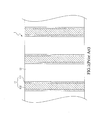
- Fig. 1 shows a schematic view of a conventional arrangement of the active region trenches.
- the semiconductor structure 1 has a plurality of active region trenches 11 and an epitaxial layer 12.
- the active region trenches 11 has an active region dielectric layer 111 and a polysilicon layer 112 located therein, and the active region trenches 11 are of continuous stripe-shaped structures regularly arranged in the epitaxial layer 12.
- continuous stripe-shaped structure restricts the effective usage of epitaxial layer 12 surface area and limits the output current under forward bias.
- a higher forward bias voltage or a larger chip size should be used, wherein the later is the method being used in the present practice to increase output current.
- neither of these methods has industrial economic efficiency.
- a major object of the present invention is to provide a semiconductor structure with dispersedly arranged active region trenches, which has a plurality of active region trenches formed in the epitaxial layer and these active region trenches are arranged in a dispersed manner.
- the semiconductor structure with dispersedly arranged active region trenches comprises a semiconductor substrate, an epitaxial layer, and an active region dielectric layer.
- the semiconductor substrate is doped with impurities of a first conductive type having a first impurity concentration.
- the epitaxial layer is doped with impurities of the first conductive type having a second impurity concentration and formed on the semiconductor substrate.
- the epitaxial layer has a plurality of active region trenches formed therein. These active region trenches are arranged in the epitaxial layer in a dispersed manner.
- the active region dielectric layer covers a bottom and a sidewall of the active region trenches.
- the active region trench has an opening in a tetragonal shape on a surface of the epitaxial layer, and the first impurity concentration is greater than the second impurity concentration.
- the tetragonal shape is a square or a rectangle, a side of the square is ranged between 0.6 ⁇ m and 1.5 ⁇ m, a length of the rectangle is ranged between 3 ⁇ m and 8 ⁇ m, and a width of the rectangle is ranged between 0.6 ⁇ m and 1.5 ⁇ m.
- an interval between central points of the active region trenches is ranged between 3 ⁇ m and 5 ⁇ m.
- an interval between length sides of the active region trenches is ranged between 1.5 ⁇ m and 5 ⁇ m, and an interval between width sides thereof is ranged between 1.5 ⁇ m and 5 ⁇ m.
- the semiconductor structure with dispersedly arranged active region trenches further comprises an ion implantation layer, which is formed in the active region trenches by implanting impurities of a second conductive type into the bottom of the active region trenches with an ion implantation power of the impurities of the second conductive type ranged between 30KeV and 100KeV, an implantation angle thereof ranged between 7 and 25 degree, and an impurity concentration thereof ranged between 1e 12 and 1e 13 .
- the semiconductor structure with dispersedly arranged active region trenches further comprises a polysilicon layer covering the active region dielectric layer and filling the active region trenches.
- a thickness of the active region dielectric layer is ranged between 1000 ⁇ and 3000 ⁇ , the active region dielectric layer may be a thermal oxide layer formed of SiO 2 .
- the semiconductor structure with dispersedly arranged active region trenches further comprises at least a termination region trench, which is formed in the epitaxial layer and away from the active region trenches.
- the termination region trench has a depth greater than that of the active region trenches and close to a depth of a depletion region under reverse breakdown.
- an interval of the termination region trench and the closest active region trench is ranged between 0.5 ⁇ m and 4 ⁇ m, a width of the termination region trench is ranged between 3 ⁇ m and 10 ⁇ m, a depth of the termination region trench is ranged between 5 ⁇ m and 12 ⁇ m, a width of the active region trenches is ranged between 0.6 ⁇ m and 1.5 ⁇ m, and a depth of the active region trenches is ranged between 1.5 ⁇ m and 3 ⁇ m.
- the semiconductor structure with dispersedly arranged active region trenches further comprises a termination region dielectric layer lining the termination region trench.
- the termination dielectric layer comprises a Tetraethoxysilane (TEOS) layer and a Boron Phosphorous Silicate Glass (BPSG) layer.
- TEOS Tetraethoxysilane
- BPSG Boron Phosphorous Silicate Glass
- a thickness of the TEOS layer is ranged between 1000 ⁇ and 3000 ⁇
- a thickness of the BPSG layer is ranged between 4000 ⁇ and 7000 ⁇ .
- a major object of the present invention is to provide a semiconductor structure with dispersedly arranged active region trenches, which has a plurality of active region trenches formed in the epitaxial layer and these active region trenches are arranged in a dispersed manner.
- Such structure is capable to increase the exposed surface area of the epitaxial layer such that a desired current output might be generated by using a smaller forward bias voltage.
- Fig. 1 is a schematic view showing a conventional arrangement of the active region trenches.
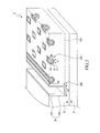
- Fig. 2 is a schematic view of a semiconductor device with dispersed arranged active region trenches in accordance with a first embodiment of the present invention.
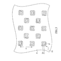
- Fig. 3 is a schematic view of an arrangement of the active region trenches in accordance with the first embodiment of the present invention.
- Fig. 4 is a schematic view of an arrangement of the active region trenches in accordance with a second embodiment of the present invention.
- Fig. 2 is a schematic view of a semiconductor structure with dispersedly arranged active region trenches in accordance with a first embodiment of the present invention
- Fig. 3 is a schematic view showing the arrangement of the active region trenches of the first embodiment of the present invention.
- the semiconductor structure 2 comprises a semiconductor substrate 21, an epitaxial layer 22, an ion implantation layer 23, an active region dielectric layer 24, a polysilicon layer 25, and a termination region dielectric layer 26.
- the semiconductor substrate 21 is doped with impurities of a first conductive type having a first impurity concentration.
- the epitaxial layer 22 is formed on the semiconductor substrate 21 and is doped with impurities of the first conductive type having a second impurity concentration, wherein the first impurity concentration is greater than the second impurity concentration.
- the first impurity concentration is labeled N+ and the second impurity concentration is labeled N- in the figures.
- the epitaxial layer 22 has a plurality of active region trenches 221 and a termination region trench 222 formed therein. These active region trenches 221 are arranged in the epitaxial layer 22 in a dispersed manner, and the termination region trench 222 is away from the active region trenches 221. In addition, a depth d1 of the active region trenches 221 is smaller than a depth d2 of the termination region trenches, and the depth d2 is close to a depth of the depletion region under reverse breakdown, which is the level of the depletion region curve 100 in this figure. As a preferred embodiment, an interval between the termination region trench 222 and the closest one of the active region trenches 221 is ranged between 0.5 ⁇ m and 4 ⁇ m.
- a width w1 of the active region trenches 221 is ranged between 0.6 ⁇ m and 1.5 ⁇ m
- the depth d1 of the active region trenches 221 is ranged between 1.5 ⁇ m and 3 ⁇ m
- a width w2 of the termination region trench 222 is ranged between 3 ⁇ m and 10 ⁇ m
- the depth d2 of the termination region trench 222 is ranged between 5 ⁇ m and 12 ⁇ m.
- the active region trench 221 has an opening in a tetragonal shape on a surface of the epitaxial layer 22.
- the tetragonal shape is a square.
- a side of the square is ranged between 0.6 ⁇ m and 1.5 ⁇ m.
- an interval r1 between central points of the active region trenches 221 is ranged between 3 ⁇ m and 5 ⁇ m.
- the ion implantation layer 23 is formed in the active region trenches 221 by implanting impurities of a second conductive type into the bottom of the active region trenches 221 with an ion implantation power of the impurities of the second conductive type ranged between 30KeV and 100KeV, an implantation angle thereof ranged between 7 and 25 degree, and an impurity concentration thereof ranged between 1e 12 and 1e 13 .
- the active region dielectric layer 24 covers a bottom and a sidewall of the active region trenches 221.
- the active region dielectric layer 24 may be a thermal oxide layer with a thickness ranged between 1000 ⁇ and 3000 ⁇ .
- the thermal oxide layer may be formed of silicon dioxide (SiO 2 ).
- the polysilicon layer 25 covers the active region dielectric layer 24 and fills the active region trenches 221.
- the termination region dielectric layer 226 lines the termination region trench 222.
- the termination dielectric layer 226 comprises a Tetraethoxysilane (TEOS) layer 261 and a Boron Phosphorous Silicate Glass (BPSG) layer 262.
- TEOS Tetraethoxysilane
- BPSG Boron Phosphorous Silicate Glass
- a thickness of the TEOS layer 261 is ranged between 1000 ⁇ and 3000 ⁇
- a thickness of the BPSG layer 262 is ranged between 4000 ⁇ and 7000 ⁇ .
- the active region trenches 221 have an opening in a square shape, and the ion implantation layer 23 would be turned into a circular-shaped ion implantation region 27 in the epitaxial layer 22 after the thermal process.
- FIG. 4 shows a schematic view of the arrangement of the active region trenches in accordance with a second embodiment of the present invention.
- these active region trenches 221' are filled with the active region dielectric layer 24' and the polysilicon layer 25', and the opening of the active region trench 221' on the surface of the epitaxial layer 22' shows a rectangular shape and these openings are arranged in an array.
- the interval r2 between the width sides of the active region trenches 221' is ranged between 1.5 ⁇ m and 5 ⁇ m
- the interval r3 between the length sides of the active region trenches 221' is ranged between 1.5 ⁇ m and 5 ⁇ m
- the length of the rectangular shape is ranged between 3 ⁇ m and 8 ⁇ m
- the width thereof is ranged between 0.6 ⁇ m and 1.5 ⁇ m.
- the exposed surface area of the epitaxial layer can be enhanced such that the semiconductor structure with dispersedly arranged active region trenches provided in the present invention is capable to generate the desired current output by using a smaller forward bias voltage. It is believed that such semiconductor structure should be able to fulfill the industrial usage.
Landscapes
- Semiconductor Integrated Circuits (AREA)
- Electrodes Of Semiconductors (AREA)
Applications Claiming Priority (1)
| Application Number | Priority Date | Filing Date | Title |
|---|---|---|---|
| TW101206869U TWM435716U (en) | 2012-04-13 | 2012-04-13 | The active region of the trench distributed arrangement of the semiconductor device structure |
Publications (1)
| Publication Number | Publication Date |
|---|---|
| EP2650921A1 true EP2650921A1 (fr) | 2013-10-16 |
Family
ID=47048206
Family Applications (1)
| Application Number | Title | Priority Date | Filing Date |
|---|---|---|---|
| EP13150623.0A Ceased EP2650921A1 (fr) | 2012-04-13 | 2013-01-09 | Structure à semi-conducteur à tranchées de région active agencées de façon dispersée |
Country Status (6)
| Country | Link |
|---|---|
| US (1) | US8779545B2 (fr) |
| EP (1) | EP2650921A1 (fr) |
| JP (1) | JP3182138U (fr) |
| KR (1) | KR200476423Y1 (fr) |
| CN (1) | CN203150558U (fr) |
| TW (1) | TWM435716U (fr) |
Families Citing this family (2)
| Publication number | Priority date | Publication date | Assignee | Title |
|---|---|---|---|---|
| CN108461550A (zh) * | 2018-02-23 | 2018-08-28 | 深圳市威兆半导体有限公司 | 一种肖特基二极管设计和制作方法 |
| CN114664926A (zh) * | 2022-03-30 | 2022-06-24 | 电子科技大学 | 一种功率半导体器件结构 |
Citations (5)
| Publication number | Priority date | Publication date | Assignee | Title |
|---|---|---|---|---|
| US6078090A (en) * | 1997-04-02 | 2000-06-20 | Siliconix Incorporated | Trench-gated Schottky diode with integral clamping diode |
| US20010010385A1 (en) * | 2000-02-02 | 2001-08-02 | U.S. Philips Corporation | Trenched schottky rectifiers |
| EP1168455A2 (fr) * | 2000-06-30 | 2002-01-02 | Kabushiki Kaisha Toshiba | Element de commutation semiconducteur a puissance |
| JP2012019188A (ja) * | 2010-06-11 | 2012-01-26 | Toyota Motor Corp | 半導体装置および半導体装置の製造方法 |
| DE202011107497U1 (de) * | 2010-12-17 | 2012-02-27 | Taiwan Semiconductor Co.,Ltd. | Struktur einer Schottky-Diode |
Family Cites Families (6)
| Publication number | Priority date | Publication date | Assignee | Title |
|---|---|---|---|---|
| GB0122120D0 (en) * | 2001-09-13 | 2001-10-31 | Koninkl Philips Electronics Nv | Edge termination in MOS transistors |
| GB0122121D0 (en) | 2001-09-13 | 2001-10-31 | Koninkl Philips Electronics Nv | Edge termination in a trench-gate mosfet |
| TW587338B (en) * | 2003-05-06 | 2004-05-11 | Mosel Vitelic Inc | Stop structure of trench type DMOS device and its formation method |
| EP2109879A4 (fr) * | 2007-01-09 | 2011-05-18 | Maxpower Semiconductor Inc | Dispositif semi-conducteur et son procédé de fabrication |
| US7989887B2 (en) * | 2009-11-20 | 2011-08-02 | Force Mos Technology Co., Ltd. | Trench MOSFET with trenched floating gates as termination |
| JP5136578B2 (ja) | 2010-03-09 | 2013-02-06 | トヨタ自動車株式会社 | 半導体装置 |
-
2012
- 2012-04-13 TW TW101206869U patent/TWM435716U/zh not_active IP Right Cessation
- 2012-12-14 CN CN2012206908505U patent/CN203150558U/zh not_active Expired - Lifetime
- 2012-12-26 KR KR2020120012238U patent/KR200476423Y1/ko not_active Expired - Lifetime
- 2012-12-27 JP JP2012007860U patent/JP3182138U/ja not_active Expired - Lifetime
-
2013
- 2013-01-09 EP EP13150623.0A patent/EP2650921A1/fr not_active Ceased
- 2013-01-09 US US13/737,233 patent/US8779545B2/en active Active
Patent Citations (5)
| Publication number | Priority date | Publication date | Assignee | Title |
|---|---|---|---|---|
| US6078090A (en) * | 1997-04-02 | 2000-06-20 | Siliconix Incorporated | Trench-gated Schottky diode with integral clamping diode |
| US20010010385A1 (en) * | 2000-02-02 | 2001-08-02 | U.S. Philips Corporation | Trenched schottky rectifiers |
| EP1168455A2 (fr) * | 2000-06-30 | 2002-01-02 | Kabushiki Kaisha Toshiba | Element de commutation semiconducteur a puissance |
| JP2012019188A (ja) * | 2010-06-11 | 2012-01-26 | Toyota Motor Corp | 半導体装置および半導体装置の製造方法 |
| DE202011107497U1 (de) * | 2010-12-17 | 2012-02-27 | Taiwan Semiconductor Co.,Ltd. | Struktur einer Schottky-Diode |
Also Published As
| Publication number | Publication date |
|---|---|
| CN203150558U (zh) | 2013-08-21 |
| US20130270669A1 (en) | 2013-10-17 |
| KR200476423Y1 (ko) | 2015-02-27 |
| JP3182138U (ja) | 2013-03-07 |
| TWM435716U (en) | 2012-08-11 |
| KR20130006137U (ko) | 2013-10-23 |
| US8779545B2 (en) | 2014-07-15 |
Similar Documents
| Publication | Publication Date | Title |
|---|---|---|
| US11610884B2 (en) | Semiconductor device | |
| CN103022156B (zh) | 带有集成肖特基势垒二极管的沟槽mosfet器件 | |
| TWI434412B (zh) | 溝槽閘極式場效電晶體及其製造方法 | |
| EP2650920B1 (fr) | Structure de semi-conducteur à tranchées | |
| CN101517752B (zh) | 具有浮岛的结势垒肖特基二极管 | |
| US9496346B2 (en) | Silicon carbide device and a method for forming a silicon carbide device | |
| US9431479B2 (en) | High breakdown voltage semiconductor device having a resurf layer | |
| US20180026129A1 (en) | Trench Edge Termination Structure for Power Semiconductor Devices | |
| JP2005093972A (ja) | 縦型半導体装置及びその製造方法 | |
| TWI657583B (zh) | 具有多重場張馳溝渠的終端結構以用於高電壓應用的溝渠式mos裝置 | |
| CN109314130B (zh) | 绝缘栅极功率半导体器件以及用于制造这种器件的方法 | |
| TWI659459B (zh) | 半導體裝置 | |
| US8564059B2 (en) | High-voltage vertical power component | |
| US20200066857A1 (en) | Semiconductor device including junction material in a trench and manufacturing method | |
| KR102795891B1 (ko) | 수퍼 정션 반도체 장치 및 이의 제조 방법 | |
| US8779545B2 (en) | Semiconductor structure with dispersedly arranged active region trenches | |
| JP5135663B2 (ja) | 半導体装置およびその製造方法 | |
| CN116598359B (zh) | 集成结势垒肖特基二极管的沟槽型mosfet器件及制造方法 | |
| CN106158955A (zh) | 功率半导体器件及其形成方法 | |
| CN116598357A (zh) | 集成肖特基二极管的沟槽型功率mosfet器件及制造方法 | |
| KR20220015695A (ko) | 수퍼 정션 반도체 장치 및 이의 제조 방법 | |
| JP2017139439A (ja) | 半導体装置及びその製造方法 | |
| JP2014060301A (ja) | 電力用半導体装置及びその製造方法 |
Legal Events
| Date | Code | Title | Description |
|---|---|---|---|
| PUAI | Public reference made under article 153(3) epc to a published international application that has entered the european phase |
Free format text: ORIGINAL CODE: 0009012 |
|
| 17P | Request for examination filed |
Effective date: 20130109 |
|
| AK | Designated contracting states |
Kind code of ref document: A1 Designated state(s): AL AT BE BG CH CY CZ DE DK EE ES FI FR GB GR HR HU IE IS IT LI LT LU LV MC MK MT NL NO PL PT RO RS SE SI SK SM TR |
|
| AX | Request for extension of the european patent |
Extension state: BA ME |
|
| 17Q | First examination report despatched |
Effective date: 20151021 |
|
| STAA | Information on the status of an ep patent application or granted ep patent |
Free format text: STATUS: THE APPLICATION HAS BEEN REFUSED |
|
| 18R | Application refused |
Effective date: 20180411 |