EP2650923B1 - Cellule solaire, module cellule solaire et methode de fabrication de cellule solaire - Google Patents
Cellule solaire, module cellule solaire et methode de fabrication de cellule solaire Download PDFInfo
- Publication number
- EP2650923B1 EP2650923B1 EP11846590.5A EP11846590A EP2650923B1 EP 2650923 B1 EP2650923 B1 EP 2650923B1 EP 11846590 A EP11846590 A EP 11846590A EP 2650923 B1 EP2650923 B1 EP 2650923B1
- Authority
- EP
- European Patent Office
- Prior art keywords
- electrode
- back side
- solar cell
- conductive paste
- dopant
- Prior art date
- Legal status (The legal status is an assumption and is not a legal conclusion. Google has not performed a legal analysis and makes no representation as to the accuracy of the status listed.)
- Active
Links
Images

Classifications
-
- H—ELECTRICITY
- H10—SEMICONDUCTOR DEVICES; ELECTRIC SOLID-STATE DEVICES NOT OTHERWISE PROVIDED FOR
- H10F—INORGANIC SEMICONDUCTOR DEVICES SENSITIVE TO INFRARED RADIATION, LIGHT, ELECTROMAGNETIC RADIATION OF SHORTER WAVELENGTH OR CORPUSCULAR RADIATION
- H10F19/00—Integrated devices, or assemblies of multiple devices, comprising at least one photovoltaic cell covered by group H10F10/00, e.g. photovoltaic modules
-
- H—ELECTRICITY
- H10—SEMICONDUCTOR DEVICES; ELECTRIC SOLID-STATE DEVICES NOT OTHERWISE PROVIDED FOR
- H10F—INORGANIC SEMICONDUCTOR DEVICES SENSITIVE TO INFRARED RADIATION, LIGHT, ELECTROMAGNETIC RADIATION OF SHORTER WAVELENGTH OR CORPUSCULAR RADIATION
- H10F71/00—Manufacture or treatment of devices covered by this subclass
- H10F71/121—The active layers comprising only Group IV materials
-
- H—ELECTRICITY
- H10—SEMICONDUCTOR DEVICES; ELECTRIC SOLID-STATE DEVICES NOT OTHERWISE PROVIDED FOR
- H10F—INORGANIC SEMICONDUCTOR DEVICES SENSITIVE TO INFRARED RADIATION, LIGHT, ELECTROMAGNETIC RADIATION OF SHORTER WAVELENGTH OR CORPUSCULAR RADIATION
- H10F10/00—Individual photovoltaic cells, e.g. solar cells
- H10F10/10—Individual photovoltaic cells, e.g. solar cells having potential barriers
- H10F10/14—Photovoltaic cells having only PN homojunction potential barriers
-
- H—ELECTRICITY
- H10—SEMICONDUCTOR DEVICES; ELECTRIC SOLID-STATE DEVICES NOT OTHERWISE PROVIDED FOR
- H10F—INORGANIC SEMICONDUCTOR DEVICES SENSITIVE TO INFRARED RADIATION, LIGHT, ELECTROMAGNETIC RADIATION OF SHORTER WAVELENGTH OR CORPUSCULAR RADIATION
- H10F71/00—Manufacture or treatment of devices covered by this subclass
- H10F71/129—Passivating
-
- H—ELECTRICITY
- H10—SEMICONDUCTOR DEVICES; ELECTRIC SOLID-STATE DEVICES NOT OTHERWISE PROVIDED FOR
- H10F—INORGANIC SEMICONDUCTOR DEVICES SENSITIVE TO INFRARED RADIATION, LIGHT, ELECTROMAGNETIC RADIATION OF SHORTER WAVELENGTH OR CORPUSCULAR RADIATION
- H10F77/00—Constructional details of devices covered by this subclass
- H10F77/20—Electrodes
- H10F77/206—Electrodes for devices having potential barriers
- H10F77/211—Electrodes for devices having potential barriers for photovoltaic cells
-
- H—ELECTRICITY
- H10—SEMICONDUCTOR DEVICES; ELECTRIC SOLID-STATE DEVICES NOT OTHERWISE PROVIDED FOR
- H10F—INORGANIC SEMICONDUCTOR DEVICES SENSITIVE TO INFRARED RADIATION, LIGHT, ELECTROMAGNETIC RADIATION OF SHORTER WAVELENGTH OR CORPUSCULAR RADIATION
- H10F77/00—Constructional details of devices covered by this subclass
- H10F77/30—Coatings
- H10F77/306—Coatings for devices having potential barriers
- H10F77/311—Coatings for devices having potential barriers for photovoltaic cells
-
- Y—GENERAL TAGGING OF NEW TECHNOLOGICAL DEVELOPMENTS; GENERAL TAGGING OF CROSS-SECTIONAL TECHNOLOGIES SPANNING OVER SEVERAL SECTIONS OF THE IPC; TECHNICAL SUBJECTS COVERED BY FORMER USPC CROSS-REFERENCE ART COLLECTIONS [XRACs] AND DIGESTS
- Y02—TECHNOLOGIES OR APPLICATIONS FOR MITIGATION OR ADAPTATION AGAINST CLIMATE CHANGE
- Y02E—REDUCTION OF GREENHOUSE GAS [GHG] EMISSIONS, RELATED TO ENERGY GENERATION, TRANSMISSION OR DISTRIBUTION
- Y02E10/00—Energy generation through renewable energy sources
- Y02E10/50—Photovoltaic [PV] energy
- Y02E10/547—Monocrystalline silicon PV cells
-
- Y—GENERAL TAGGING OF NEW TECHNOLOGICAL DEVELOPMENTS; GENERAL TAGGING OF CROSS-SECTIONAL TECHNOLOGIES SPANNING OVER SEVERAL SECTIONS OF THE IPC; TECHNICAL SUBJECTS COVERED BY FORMER USPC CROSS-REFERENCE ART COLLECTIONS [XRACs] AND DIGESTS
- Y02—TECHNOLOGIES OR APPLICATIONS FOR MITIGATION OR ADAPTATION AGAINST CLIMATE CHANGE
- Y02P—CLIMATE CHANGE MITIGATION TECHNOLOGIES IN THE PRODUCTION OR PROCESSING OF GOODS
- Y02P70/00—Climate change mitigation technologies in the production process for final industrial or consumer products
- Y02P70/50—Manufacturing or production processes characterised by the final manufactured product
Definitions
- This invention relates to a solar cell and solar cell module having the advantages of low cost and high efficiency, and to a method of making said solar cell.
- FIG. 1 illustrates one general solar cell of mass production model using a mono- or polycrystalline silicon substrate.
- the solar cell includes a p-type silicon substrate 101 obtained by doping monocrystalline silicon with a dopant such as B or Ga.
- An emitter layer 102 is formed in a light-receiving surface of silicon substrate 101 by heat treatment to diffuse a dopant for imparting n-type conductivity such as P or Sb into silicon substrate 101 in a high concentration.
- a plurality of extraction electrodes 104 of several hundreds to several tens of microns ( ⁇ m) wide are disposed contiguous to the emitter layer 102 for extracting photogenerated electric charge from substrate 101.
- collector electrodes 105 of several millimeters (mm) wide are disposed for collecting the charges drawn in extraction electrodes 104 and interconnecting solar cells together. While these electrodes may be formed by various methods, one method commonly employed from the standpoint of cost is by printing a metal paste comprising fine particles of metal such as Ag and an organic binder through a screen or the like, and heat treating at a temperature of several hundreds to about 850°C for bonding to the substrate.
- the passivation film also has a further important function of passivating the silicon surface.
- silicon atoms are in a stable state due to the covalent bond between adjacent atoms.
- an unstable energy level known as "dangling bond" appears at the surface corresponding to the terminus of atom arrangement, where no adjacent atom to be bonded is available. Since the dangling bond is electrically active, it captures and extinguishes charge photogenerated within silicon, detracting from the operation of a solar cell.
- the solar cells have been subjected to surface passivating treatment or otherwise treated to form an electric field such that photogenerated carriers may not be captured by dangling bonds.
- a silicon nitride film formed by CVD is widely used because its optical properties are suited for silicon solar cells and because the film itself has a positive fixed charge and also has a high passivation effect due to the inclusion of much hydrogen capable of passivating dangling bonds.
- the dopant concentration of the emitter layer should desirably be kept as low as possible or the depth of the emitter layer should desirably be shallow. However, reducing the dopant concentration, in turn, increases the contact resistance between silicon and metal electrode, giving rise to the problem of an increased resistance loss of generated power.
- the localized doping structure or double doping structure is generally formed by forming a dielectric film of several hundreds of nanometers (nm) such as a silicon oxide or silicon nitride film on substrate surface as diffusion barrier, opening an electrode-forming portion of the dielectric film by photolithography (see, for example, J. Knobloch, A. Noel, E. Schaffer, U. Schubert, F. J. Kamerewerd, S. Klussmann, W. Wettling, Proc.
- One simpler method suited for mass production is by premixing a dopant in a conductive paste as the electrode-forming material, as proposed in, for example, D. L. Meier, H. P. Davis, R. A. Garcia, J. A. Jessup, Proc. the 28th IEEE Photovoltaic Specialists Conference, p.69, 2000 .
- P is added to Ag paste as dopant, for example, the paste is printed onto a silicon substrate, and the paste is fired at or above the eutectic point of Ag and Si.
- the self-doping paste contains a dopant for forming a self-doped region, an additive for effectively forming a high-concentration doping layer, and the like in relatively high proportions. For this reason, while the self-doping paste provides a good electrical contact between electrode and silicon, the content of metal particles contributing to the conduction of charge extracted from the silicon substrate must be kept low. As a result, the sintered body of self-doping paste has a high interconnect resistance, giving rise to the problem that the output of the solar cell is reduced
- the inventors have found that if a first electrode in the form of a sintered body of conductive paste containing a dopant for imparting conductivity to silicon is used as the extraction electrode, and a second electrode having a higher conductivity than the first electrode is used as the collector electrode, then the loss by contact resistance between silicon substrate and the extraction electrode and the loss by electrode resistance are reduced and solar cell characteristics are drastically improved.
- the invention is predicated on this finding.
- the invention provides a solar cell, a solar cell module and a method of making a solar cell, as defined in the appended claims.
- FIG. 2 illustrates a solar cell in one embodiment of the invention.
- the solar cell includes a crystalline silicon substrate 201 of one conductivity type, an emitter layer 202 formed on the silicon substrate 201 and having a dopant of opposite conductivity type added thereto, a passivation film 203 formed on the surface of the emitter layer 202, an extraction electrode for extracting photogenerated electric charge from the silicon substrate 201, and a collector electrode for collecting the charge drawn in the extraction electrode, wherein the electrodes are formed by printing and firing conductive paste.
- the extraction electrode includes a first electrode 204 in the form of a sintered body of conductive paste containing a dopant for imparting the same conductivity type as the emitter layer to silicon.
- the first electrode 204 is formed so as to penetrate through the passivation layer 203, and at the same time, a self-doped region 208 into which the dopant from the first electrode 204 is diffused at a high concentration is formed immediately below the first electrode 204.
- This enables to establish a good electrical contact between the first electrode 204 and the silicon substrate 201 and to reduce the dopant concentration or depth of the emitter layer 202, and eventually to ameliorate any degradation of solar cell characteristics due to carrier recombination and free carrier absorption in the emitter layer.
- the collector electrode includes a second electrode 205 having a higher conductivity than the first electrode 204, which enables to significantly reduce the output power loss of the solar cell by interconnect resistance.
- an electric field layer 206 and a back electrode 207 are illustrated.
- the texture is an effective means for lowering the reflectivity of solar cells.
- the texture may be readily provided by immersing the substrate in a hot alkaline solution of sodium hydroxide, potassium hydroxide, potassium carbonate, sodium carbonate, sodium hydrogencarbonate or tetramethylammonium hydroxide (concentration 1 to 10 wt%) at a temperature of 60 to 100°C for about 10 to about 30 minutes. Often, a proper amount of 2-propanol is dissolved in the alkaline solution to control the reaction.
- an emitter layer is formed by vapor phase diffusion using phosphorus oxychloride.
- the P concentration and depth of the emitter layer are determined by a balance of resistance to current flow through the emitter layer and surface passivation effect, or the like. Typically, they are determined such that the emitter layer may have a sheet resistance of 50 to 400 ohm/square ( ⁇ / ⁇ ) as measured by the four probe method.
- the film is not limited to silicon nitride, and instead, silicon oxide, silicon carbide, aluminum oxide, amorphous silicon, microcrystalline silicon or titanium oxide may be used while it may be formed by heat treatment, atomic layer deposition or the like as well as chemical vapor deposition.
- a first electrode is formed on the emitter layer.
- a silver paste is used which is prepared by mixing silver powder, glass frit and dopant with an organic binder.
- the dopant used herein is a Group V element such as P, In or Sb alone or a compound thereof or a combination thereof.
- the composition of the paste must be adjusted depending on the structure and type of a solar cell. When diphosphorus pentoxide is used, for example, it is formulated in a proportion of about 0.1 to 30% by weight, preferably 2 to 15% by weight.
- the type and amount of the organic binder are well known.
- the paste is screen printed and fired or heat treated to establish conduction between the electrode and the silicon.
- This heat treatment is known as a fire-through phenomenon that during firing of silver paste, the silicon nitride film reacts with the glass frit and is thus decomposed, allowing the Ag particles to penetrate through the silicon nitride film to make electrical contact with the substrate.
- the fire-through technique is widely used in the manufacture of crystalline silicon solar cells.
- the dopant in the silver paste diffuses, in part, into the silicon substrate to achieve self-doping even on heat treatment at a temperature of about 700 to 800°C in the electrode firing temperature range commonly employed, firing at a temperature equal to or higher than 835°C, the eutectic point of Ag and Si, is recommended in order to form a self-doped region more effectively.
- silicon reacts with silver and melts, and then recrystallizes while taking in additive dopant. As such, high concentration doping is accomplished, making a better electrical contact between the sintered silver and silicon.
- the dopant concentration may be directly measured by secondary ion mass spectroscopy (SIMS) or the like. This quantitative measurement, however, is scarcely used in the production site because preparation of a sample is cumbersome and measurement requires skill.
- SIMS secondary ion mass spectroscopy
- the resistivity of the region at its surface should preferably be 10 m ⁇ -cm or less, more preferably 2 m ⁇ -cm or less.
- the lower limit is usually at least 0.5 m ⁇ -cm though not critical.
- the resistivity of the emitter layer (formed in the light-receiving area) at its surface should preferably be as high as possible from the standpoint of suppressing the aforementioned optical loss and carrier recombination loss, but should preferably be somewhat low from the standpoint of increasing the photovoltage. That is, the resistivity of the emitter layer at its surface should fall in an optimum range. The optimum range is 5 to 50 m ⁇ -cm though it varies with the structure of a solar cell. On the other hand, to take the maximum advantage of dual doping structure, the emitter layer should be designed and controlled such that the resistivity of the emitter layer at its surface may be higher than the resistivity of the self-doped region.
- a second electrode is formed on the first electrode by screen printing and firing.
- the second electrode should be endowed with a higher conductivity than the first electrode for the purpose of suppressing the interconnect resistance loss when the charge extracted from the silicon substrate to the first electrode flows to the collector electrode.
- Such an electrode is prepared using a silver paste containing a higher proportion of silver particles.
- the resistivity of the second electrode which is preferably lower should desirably be up to 5 ⁇ -cm at most, more preferably up to 3 ⁇ -cm.
- the extraction electrode may have a laminate structure consisting of first and second electrodes, and the collector electrode have a monolayer structure consisting of a second electrode as shown in FIG. 2 .
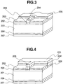
- the extraction electrode may have a monolayer structure consisting of a first electrode, and the collector electrode have a monolayer structure consisting of a second electrode, as shown in FIG. 3 .
- the extraction electrode and collector electrode each may have a laminate structure consisting of first and second electrodes as shown in FIG. 4 .
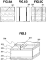
- the structure of these electrodes may be prepared, for example, by screen printing an electrode paste to form, in case of the first electrode, a pattern consisting solely of extraction electrodes as shown in FIG. 5(a) , or a pattern of both extraction and collector electrodes as shown in FIG. 5(c) , and in case of the second electrode, a pattern as shown in FIG. 5(c) or a pattern consisting solely of collector electrodes as shown in FIG. 5(b) .
- the electrode forming method is not limited to screen printing and may be performed by inkjet printing, dispenser, intaglio printing, aerosol spraying or the like.
- An electrode having a structure as shown in FIG. 4 may be prepared by effecting metallization, with the first electrode serving as seed, to form the second electrode.
- electroplating, electroless plating or photo-plating is applicable.
- the second electrode may penetrate through the passivation layer 203, for example, by fire-through capability, until it contacts the emitter layer 202, as shown in FIGS. 2 and 3 , or may not penetrate through the passivation layer 203 as shown in FIG. 6 .
- the embodiment of FIG. 6 wherein the passivation film immediately below the collector electrode is left intact inhibits recombination of carriers at the silicon surface in this portion, thus improving solar cell characteristics.
- the fire-through capability of electrode paste to penetrate through the passivation film is tailored by the amount of low-softening-point glass frit added.
- the second electrode may be formed using a high-temperature firing paste containing a relatively small amount of glass frit or free of glass frit, or a low-temperature cure resin paste.
- the back electrode is formed by mixing aluminum powder with an organic binder and screen printing the resulting paste. Printing is followed by firing at a temperature of 700 to 900°C for 5 to 30 minutes to form the back electrode and an electric field layer.
- the electric field layer may also be formed by vapor phase diffusion of boron bromide, for example. In this case, it is preferred from the standpoint of suppressing interconnect resistance to use silver paste to form the back electrode.
- Firing of the back electrode and the light-receiving surface electrode may be performed at a time. Also, the order of forming electrodes on opposite surfaces may be reversed.
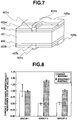
- FIG. 7 illustrates an embodiment wherein the electrode of the invention is applied to both the light-receiving surface and the non-light-receiving surface.
- the p-type silicon solar cell uses the silicon substrate 401 of p-type conductivity
- this embodiment is such that the self-doped region 407b formed immediately below the non-light-receiving side first electrode 404b is of p-type conductivity and the self-doped region 407a on the light-receiving side is of n-type conductivity.
- a self-doping paste containing a Group V element is used for the light-receiving side first electrode 404a and a self-doping paste containing a Group III element is used for the non-light-receiving side first electrode 404b.
- an emitter layer 402 is also illustrated.
- a passivation layer 403a is also illustrated.
- collector electrodes 405a and 405b are also illustrated.
- Such a structure on the non-light-receiving side allows the non-electrode-forming surface to be covered with the electric field layer 406 and passivation film 403b, enhancing the collection efficiency of photogenerated carriers. It is noted that the electric field layer 406 may not be formed where the passivation film has a fully high passivation effect.
- the second electrode 405b may penetrate through the passivation layer 403b until it contacts the field effect layer 406 or silicon substrate 401, as shown in FIG. 7 , or may not penetrate through the passivation layer.
- a reflector (not shown) is preferably provided for taking in again the light transmitted by the substrate.
- the reflector may be a film of aluminum or silver formed by vacuum evaporation or the like, a sufficient reflector effect is obtainable simply by using a white backsheet or the like on the solar cell module without any additional treatment. Absent the reflector, electricity generation is yet possible by causing scattering light to enter from the back surface or by placing the solar cell such that the non-light-receiving surface may become a light-receiving side.
- the solar cell of the invention is described by referring to the embodiments using p-type silicon substrates, the invention is equally applicable to a solar cell using an n-type silicon substrate.
- silicon substrate 401, electric field layer 406 and self-doped region 407b on the non-light-receiving side are of n type and the emitter layer 402 and self-doped region 407a on the light-receiving side are of p type.
- the silicon substrate 401 is a n-type crystalline silicon substrate which is prepared by doping high-purity silicon with a Group V element such as P or Sb to give a resistivity of 0.1 to 5 Q-cm.
- the emitter layer 402 may be formed when the silicon substrate is doped with boron by vapor phase diffusion using boron bromide, for example.
- the electric field layer may be formed by vapor phase diffusion using phosphorus oxychloride, for example.
- the self-doped layer 407a on the light-receiving side is formed using a self-doping paste containing a Group III element such as B, A1, Ga or In alone or a compound thereof or a combination thereof.
- the self-doped layer 407b on the non-light-receiving side is formed using a self-doping paste containing a Group V element such as P, As or Sb alone or a compound thereof or a combination thereof.
- a plurality of solar cells according to the invention may be electrically connected and used as a solar cell module.
- the connection may be made by any well-known methods.
- a solar cell having a conventional electrode structure and a solar cell having an electrode structure according to the invention are compared for electricity generating ability.
- a silicon nitride film was formed over the sample surface on the light-receiving side as a passivation film.
- the substrates were divided into three groups (1), (2) and (3), each consisting of 30 substrates.
- Each of different silver pastes (see below) was printed on the substrates as a light-receiving side electrode using a printing screen having a pattern of extraction and collector electrodes on a common screen as shown in FIG. 5(c) .
- printing conditions such as printing pressure and squeeze angle were controlled such that an equivalent line width and cross-sectional area were obtained at the end of firing.
- Group (1) is a comparative example by the prior art technique.
- first electrode ordinary fire-through type high-temperature firing paste (paste A) was screen printed and dried.
- paste B high-conductivity silver paste
- firing at 830°C or optimum condition was carried out in the ambient (air) atmosphere.
- Group (2) is another comparative example by the prior art technique.
- fire-through type self-doping silver paste (paste C) having a phosphorus compound added so that the self-doped region might have a resistivity of 2 m ⁇ -cm was screen printed and dried.
- paste C was again screen printed as the second electrode so that the first electrode was completely overlaid therewith. Thereafter, firing at 880°C or optimum condition was carried out in the ambient atmosphere.
- Determination of contact resistance was by the ladder method.
- Determination of interconnect resistance was carried out by cutting out an extraction electrode portion from the solar cell sample, placing probes at opposite ends of the electrode and measuring current-voltage values.
- FIG. 8 illustrates relative values of the two resistances for each group, provided that the average value of samples of group (1) is 1. It is seen that the samples of group (3) having the electrode structure according to the invention have a low contact resistance. It is thus concluded that the samples of group (3) show the highest fill factor in Table 2 as a result of the contact resistance and interconnect resistance being suppressed.
Landscapes
- Photovoltaic Devices (AREA)
- Life Sciences & Earth Sciences (AREA)
- Sustainable Development (AREA)
- Engineering & Computer Science (AREA)
- Sustainable Energy (AREA)
- Electrodes Of Semiconductors (AREA)
- Chemical & Material Sciences (AREA)
- Crystallography & Structural Chemistry (AREA)
Claims (16)
- Cellule solaire comprenant un substrat de silicium cristallin (201, 401) d'un type de conductivité ayant une surface de réception de lumière, une couche émettrice (202, 402) formée sur le côté surface de réception de lumière du substrat et ayant un dopant d'un type de conductivité opposé ajouté à celle-ci, un film de passivation (203, 403a) formé sur la surface du substrat, une électrode d'extraction pour extraire une charge photo-générée du substrat de silicium, et une électrode collectrice en contact avec au moins une partie de l'électrode d'extraction pour collecter la charge attirée dans l'électrode d'extraction, dans laquelle
l'électrode d'extraction inclut une première électrode (204, 404a), l'électrode collectrice inclut une seconde électrode (205, 405a), et la première électrode (204, 404a) est partiellement en contact ou entièrement recouverte avec la seconde électrode (205, 405),
caractérisée en ce que
la première électrode est sous une forme pouvant être obtenue par frittage d'une pâte conductrice contenant de la poudre d'argent, de la fritte de verre et un dopant pour conférer une conductivité au silicium, la première électrode (204, 404a) pénétrant à travers le film de passivation (203, 403a), moyennant quoi en dessous de l'interface entre la couche émettrice (202, 402) et la première électrode (204, 404a), se trouve une région auto-dopée (208, 407a) en résultat de la diffusion de dopant supplémentaire à partir de la première électrode pendant le frittage, et
l'électrode collectrice inclut une seconde électrode (205, 405a) pouvant être obtenue par cuisson d'une pâte conductrice contenant une proportion plus élevée de poudre d'argent que ladite pâte conductrice formant la première électrode, et ayant une conductivité plus élevée que la première électrode (204, 404a). - Cellule solaire selon la revendication 1, dans laquelle la région auto-dopée (208, 407a) a une résisitivité plus faible que la couche émettrice (202, 402) disposée de manière adjacente à celle-ci.
- Cellule solaire selon la revendication 1 ou la revendication 2, dans laquelle la première électrode (204, 404a) est formée d'une pâte conductrice à base de Ag et contenant B, Al, Ga, P, As, In ou Sb, seuls ou sous forme d'un composé de ceux-ci ou d'une combinaison de ceux-ci, en tant que dopant.
- Cellule solaire selon l'une quelconque des revendications 1 à 3, dans laquelle l'électrode d'extraction a une structure stratifiée constituée des première et seconde électrodes (204, 205 ; 404a, 405), et l'électrode collectrice a une structure monocouche constituée de la seconde électrode (205, 405).
- Cellule solaire selon l'une quelconque des revendications 1 à 3, dans laquelle l'électrode d'extraction et l'électrode collectrice ont chacune une structure stratifiée constituée des première et seconde électrodes (204, 405).
- Cellule solaire selon l'une quelconque des revendications 1 à 3, dans laquelle l'électrode d'extraction est constituée de la première électrode (204) et l'électrode collectrice est constituée de la seconde électrode (205) .
- Cellule solaire selon l'une quelconque des revendications 1 à 6, dans laquelle le film de passivation comprend de l'oxyde de silicium, du nitrure de silicium, du carbure de silicium, de l'oxyde d'aluminium, du silicium amorphe, du silicium microcristallin ou de l'oxyde de titane ou une combinaison de ceux-ci.
- Cellule solaire selon l'une quelconque des revendications 1 à 7, dans laquelle le substrat de silicium cristallin a une surface non réceptrice de lumière avec un film de passivation de côté arrière (403b) formé sur la surface non réceptrice de lumière du substrat, une électrode d'extraction de côté arrière pour extraire une charge photo-générée du substrat de silicium, et une électrode collectrice de côté arrière disposée au moins partiellement en contact avec l'électrode d'extraction de côté arrière pour collecter la charge collectée dans l'électrode d'extraction de côté arrière, et dans laquelle
l'électrode d'extraction de côté arrière inclut une première électrode de côté arrière (404b) pouvant être obtenue par frittage d'une pâte conductrice contenant un dopant pour conférer une conductivité au silicium, la première électrode de côté arrière (404b) pénétrant à travers le film de passivation de côté arrière (403b), moyennant quoi à l'interface entre le substrat de silicium et la première électrode de côté arrière, se trouve une région auto-dopée (407b) en résultat d'une diffusion de dopant dans la première électrode de côté arrière pendant le frittage,
l'électrode collectrice côté de arrière inclut une seconde électrode de côté arrière (405b) ayant une conductivité plus élevée que la première électrode de côté arrière (404b), et
la première électrode de côté arrière (404b) est partiellement en contact ou entièrement recouverte avec la seconde électrode de côté arrière (405b). - Cellule solaire selon la revendication 8, dans laquelle la première électrode de côté arrière (404b) peut être obtenue par frittage d'une dite pâte conductrice contenant de la poudre d'argent, de la fritte de verre et ledit dopant et la seconde électrode de côté arrière (405b) peut être obtenue par frittage d'une pâte conductrice contenant une proportion plus élevée de poudre d'argent que ladite pâte conductrice formant la première électrode de côté arrière.
- Cellule solaire selon la revendication 8, dans laquelle la région auto-dopée (407b) au niveau de la surface non réceptrice de lumière a une résisitivité plus faible qu'une région non auto-dopée disposée de manière adjacente à celle-ci.
- Module de cellules solaires comprenant des cellules solaires connectées électriquement selon l'une quelconque des revendications 1 à 10.
- Procédé de fabrication d'une cellule solaire selon l'une quelconque des revendications 1 à 10, comprenant(a) sur ledit côté surface de réception de lumière du substrat de silicium cristallin, la formation d'une couche émettrice (202, 402) par ajout de dopant, et la formation du film de passivation (203, 403a) sur ladite surface du substrat, et caractérisé par(b) la formation de la première électrode (204, 404a) par frittage d'une dite pâte conductrice contenant de la poudre d'argent, de la fritte de verre et ledit dopant pour conférer une conductivité au silicium, moyennant quoi pendant ledit frittage la pâte conductrice pénètre dans le film de passivation (203, 403a) pour établir un contact électrique avec le substrat de silicium, et le dopant dans la pâte conductrice se diffuse pour former la région auto-dopée (208, 407a) en dessous de l'interface entre la première électrode (204, 404a) et la couche émettrice, etla formation de la seconde électrode (405a) par cuisson de ladite pâte conductrice contenant une proportion plus élevée de poudre d'argent que ladite pâte conductrice formant la première électrode (404b).
- Procédé selon la revendication 12, dans lequel pour fournir les première et seconde électrodes, la première électrode est imprimée et séchée, la seconde électrode est imprimée, et un traitement thermique unique est réalisé pour faire cuire à la fois les première et seconde électrodes en même temps.
- Procédé selon la revendication 12 ou 13, dans lequel la première électrode (204, 404a) est préparée par sérigraphie de la pâte d'électrode conductrice pour former un motif d'électrodes d'extraction uniquement ou un motif à la fois d'électrodes d'extraction et collectrices, et la seconde électrode (204, 404a) est préparée par sérigraphie de pâte d'électrode conductrice pour former un motif à la fois d'électrodes d'extraction et collectrices ou un motif d'électrodes collectrices uniquement.
- Procédé selon l'une quelconque des revendications 12 à 14 fabriquant une cellule solaire selon la revendication 8, et comprenant :(c) sur ladite surface non réceptrice de lumière du substrat de silicium cristallin, la formation dudit film de passivation de côté arrière (403b), et(d) la formation de la première électrode de côté arrière (404b) par frittage de ladite pâte conductrice contenant du dopant pour procurer une conductivité au silicium, moyennant quoi pendant ledit frittage, la pâte conductrice pénètre dans le film de passivation de côté arrière (403b) et le dopant dans la pâte conductrice se diffuse pour former la région auto-dopée (407b) à l'interface entre la première électrode de côté arrière (404b) et le substrat de silicium, etla formation de la seconde électrode de côté arrière (405b) ayant une conductivité plus élevée que la première électrode de côté arrière (404b).
- Procédé selon la revendication 15, dans lequel la première électrode de côté arrière (404b) est formée par frittage d'une dite pâte conductrice contenant de la poudre d'argent, de la fritte de verre et ledit dopant, et la seconde électrode de côté arrière (405b) est formée par cuisson d'une pâte conductrice contenant une proportion plus élevée de poudre d'argent que ladite pâte conductrice formant la première électrode de côté arrière.
Applications Claiming Priority (2)
| Application Number | Priority Date | Filing Date | Title |
|---|---|---|---|
| JP2010271619 | 2010-12-06 | ||
| PCT/JP2011/077784 WO2012077567A1 (fr) | 2010-12-06 | 2011-12-01 | Cellule solaire et module cellule solaire |
Publications (3)
| Publication Number | Publication Date |
|---|---|
| EP2650923A1 EP2650923A1 (fr) | 2013-10-16 |
| EP2650923A4 EP2650923A4 (fr) | 2017-11-22 |
| EP2650923B1 true EP2650923B1 (fr) | 2021-06-02 |
Family
ID=46207057
Family Applications (1)
| Application Number | Title | Priority Date | Filing Date |
|---|---|---|---|
| EP11846590.5A Active EP2650923B1 (fr) | 2010-12-06 | 2011-12-01 | Cellule solaire, module cellule solaire et methode de fabrication de cellule solaire |
Country Status (12)
| Country | Link |
|---|---|
| US (2) | US20130247957A1 (fr) |
| EP (1) | EP2650923B1 (fr) |
| JP (1) | JP5541370B2 (fr) |
| KR (1) | KR101917879B1 (fr) |
| CN (1) | CN103329280B (fr) |
| CA (1) | CA2820002A1 (fr) |
| MY (1) | MY170106A (fr) |
| PH (1) | PH12013501162A1 (fr) |
| RU (1) | RU2571444C2 (fr) |
| SG (1) | SG191044A1 (fr) |
| TW (1) | TWI587534B (fr) |
| WO (1) | WO2012077567A1 (fr) |
Families Citing this family (19)
| Publication number | Priority date | Publication date | Assignee | Title |
|---|---|---|---|---|
| US9293624B2 (en) * | 2012-12-10 | 2016-03-22 | Sunpower Corporation | Methods for electroless plating of a solar cell metallization layer |
| US9263601B2 (en) * | 2012-12-21 | 2016-02-16 | Sunpower Corporation | Enhanced adhesion of seed layer for solar cell conductive contact |
| KR102032280B1 (ko) * | 2013-04-25 | 2019-10-15 | 엘지전자 주식회사 | 태양 전지의 전극용 페이스트 조성물 |
| US20160104810A1 (en) * | 2013-05-13 | 2016-04-14 | Kaneka Corporation | Solar cell module and method for producing same |
| US9761752B2 (en) | 2013-05-21 | 2017-09-12 | Kaneka Corporation | Solar cell, solar cell module, method for manufacturing solar cell, and method for manufacturing solar cell module |
| JP2015050349A (ja) * | 2013-09-02 | 2015-03-16 | 株式会社ノリタケカンパニーリミテド | 太陽電池素子およびその製造方法並びにファイヤースルー用アルミニウムペースト |
| TW201511300A (zh) * | 2013-09-11 | 2015-03-16 | 行政院原子能委員會核能研究所 | 具有摻雜矽或硼原子之鋁金屬電極之製備方法 |
| KR101867855B1 (ko) | 2014-03-17 | 2018-06-15 | 엘지전자 주식회사 | 태양 전지 |
| US20170117433A1 (en) * | 2014-04-03 | 2017-04-27 | Trina Solar Energy Development Pte Ltd | A hybrid all-back-contact solar cell and method of fabricating the same |
| CN104241454B (zh) * | 2014-09-25 | 2017-04-05 | 上海联孚新能源科技集团有限公司 | 一种提高太阳能电池转化效率的方法 |
| JP6502651B2 (ja) | 2014-11-13 | 2019-04-17 | 信越化学工業株式会社 | 太陽電池の製造方法及び太陽電池モジュールの製造方法 |
| US10061450B2 (en) | 2014-12-04 | 2018-08-28 | Apple Inc. | Coarse scan and targeted active mode scan for touch |
| CN110100317B (zh) * | 2016-12-13 | 2022-09-30 | 信越化学工业株式会社 | 高效背面接触型太阳能电池单元、太阳能电池组件和光伏发电系统 |
| CN110047952A (zh) * | 2019-04-04 | 2019-07-23 | 国家电投集团西安太阳能电力有限公司 | 一种太阳能电池Al栅线结构及其制备方法 |
| WO2021075130A1 (fr) * | 2019-10-18 | 2021-04-22 | 株式会社エネコートテクノロジーズ | Élément |
| CN111739985B (zh) * | 2020-08-21 | 2021-01-12 | 浙江晶科能源有限公司 | 太阳能电池及其选择性发射极的制备方法 |
| CN112002775B (zh) * | 2020-09-08 | 2024-11-08 | 中国科学院力学研究所 | 一种激光无线充电接收端 |
| CN113644145B (zh) | 2021-10-18 | 2022-02-18 | 浙江晶科能源有限公司 | 太阳能电池及光伏组件 |
| CN121038431B (zh) * | 2025-10-30 | 2026-02-24 | 浙江晶科能源有限公司 | 太阳能电池及其制造方法、叠层电池和光伏组件 |
Family Cites Families (32)
| Publication number | Priority date | Publication date | Assignee | Title |
|---|---|---|---|---|
| JPH0536998A (ja) * | 1991-07-30 | 1993-02-12 | Sharp Corp | 電極の形成方法 |
| JP2928433B2 (ja) * | 1993-02-23 | 1999-08-03 | シャープ株式会社 | 光電変換素子の製造方法 |
| CA2232857C (fr) * | 1995-10-05 | 2003-05-13 | Jalal Salami | Pile solaire a emetteur localement profondement diffuse auto-aligne |
| JP2000138386A (ja) | 1998-11-04 | 2000-05-16 | Shin Etsu Chem Co Ltd | 太陽電池の製造方法およびこの方法で製造された太陽電池 |
| US6632730B1 (en) * | 1999-11-23 | 2003-10-14 | Ebara Solar, Inc. | Method for self-doping contacts to a semiconductor |
| AU4251001A (en) | 2000-04-28 | 2001-11-12 | Merck Patent Gmbh | Etching pastes for inorganic surfaces |
| JP2002217434A (ja) * | 2001-01-19 | 2002-08-02 | Sharp Corp | 太陽電池、太陽電池用インターコネクターおよびストリング |
| JP2004273826A (ja) | 2003-03-10 | 2004-09-30 | Sharp Corp | 光電変換装置及びその製造方法 |
| JP4121928B2 (ja) | 2003-10-08 | 2008-07-23 | シャープ株式会社 | 太陽電池の製造方法 |
| JPWO2005109524A1 (ja) * | 2004-05-07 | 2008-03-21 | 三菱電機株式会社 | 太陽電池及びその製造方法 |
| JP4557622B2 (ja) * | 2004-07-29 | 2010-10-06 | 京セラ株式会社 | 太陽電池素子の接続構造及びこれを含む太陽電池モジュール |
| JP4780953B2 (ja) | 2004-11-29 | 2011-09-28 | 京セラ株式会社 | 太陽電池素子及び、これを用いた太陽電池モジュール |
| US7435361B2 (en) | 2005-04-14 | 2008-10-14 | E.I. Du Pont De Nemours And Company | Conductive compositions and processes for use in the manufacture of semiconductor devices |
| JP2008204967A (ja) * | 2005-05-31 | 2008-09-04 | Naoetsu Electronics Co Ltd | 太陽電池素子及びその製造方法 |
| JP2007096040A (ja) | 2005-09-29 | 2007-04-12 | Sharp Corp | 太陽電池の製造方法および太陽電池 |
| US7765949B2 (en) * | 2005-11-17 | 2010-08-03 | Palo Alto Research Center Incorporated | Extrusion/dispensing systems and methods |
| JP2007214372A (ja) | 2006-02-09 | 2007-08-23 | Sharp Corp | 太陽電池およびその製造方法 |
| JP4963866B2 (ja) | 2006-04-28 | 2012-06-27 | シャープ株式会社 | 光電変換素子の製造方法 |
| TWI487124B (zh) * | 2006-08-25 | 2015-06-01 | Sanyo Electric Co | 太陽電池模組及太陽電池模組的製造方法 |
| RU2468475C2 (ru) * | 2007-07-26 | 2012-11-27 | Университет Констанц | Способ изготовления кремниевого солнечного элемента (варианты) и соответствующий солнечный элемент |
| US8309844B2 (en) * | 2007-08-29 | 2012-11-13 | Ferro Corporation | Thick film pastes for fire through applications in solar cells |
| JP4610630B2 (ja) * | 2008-03-31 | 2011-01-12 | 三菱電機株式会社 | 太陽電池用拡散層の製造方法および太陽電池セルの製造方法 |
| US20090250108A1 (en) * | 2008-04-02 | 2009-10-08 | Applied Materials, Inc. | Silicon carbide for crystalline silicon solar cell surface passivation |
| KR100974221B1 (ko) | 2008-04-17 | 2010-08-06 | 엘지전자 주식회사 | 레이저 어닐링을 이용한 태양전지의 선택적 에미터형성방법 및 이를 이용한 태양전지의 제조방법 |
| JP5172480B2 (ja) * | 2008-06-04 | 2013-03-27 | シャープ株式会社 | 光電変換装置およびその製造方法 |
| TWI423462B (zh) * | 2008-10-22 | 2014-01-11 | Ind Tech Res Inst | 矽晶太陽電池之背面電極製造方法 |
| WO2010056826A1 (fr) * | 2008-11-14 | 2010-05-20 | Applied Nanotech Holdings, Inc. | Encres et pâtes pour la fabrication de cellules solaires |
| KR100993511B1 (ko) * | 2008-11-19 | 2010-11-12 | 엘지전자 주식회사 | 태양 전지 및 그 제조 방법 |
| KR101002282B1 (ko) * | 2008-12-15 | 2010-12-20 | 엘지전자 주식회사 | 태양 전지 및 그 제조 방법 |
| CN102396073B (zh) * | 2009-04-14 | 2015-09-09 | 三菱电机株式会社 | 光电动势装置及其制造方法 |
| KR101009422B1 (ko) * | 2009-04-14 | 2011-01-19 | (유)에스엔티 | 태양전지의 제조 방법 |
| US8586129B2 (en) * | 2010-09-01 | 2013-11-19 | Solarworld Innovations Gmbh | Solar cell with structured gridline endpoints and vertices |
-
2011
- 2011-12-01 US US13/991,978 patent/US20130247957A1/en not_active Abandoned
- 2011-12-01 CA CA2820002A patent/CA2820002A1/fr not_active Abandoned
- 2011-12-01 JP JP2012547809A patent/JP5541370B2/ja active Active
- 2011-12-01 EP EP11846590.5A patent/EP2650923B1/fr active Active
- 2011-12-01 MY MYPI2013002043A patent/MY170106A/en unknown
- 2011-12-01 WO PCT/JP2011/077784 patent/WO2012077567A1/fr not_active Ceased
- 2011-12-01 CN CN201180065728.7A patent/CN103329280B/zh active Active
- 2011-12-01 RU RU2013131015/28A patent/RU2571444C2/ru active
- 2011-12-01 KR KR1020137017430A patent/KR101917879B1/ko active Active
- 2011-12-01 SG SG2013043831A patent/SG191044A1/en unknown
- 2011-12-01 PH PH1/2013/501162A patent/PH12013501162A1/en unknown
- 2011-12-06 TW TW100144862A patent/TWI587534B/zh active
-
2015
- 2015-10-23 US US14/921,473 patent/US9887312B2/en active Active
Non-Patent Citations (1)
| Title |
|---|
| None * |
Also Published As
| Publication number | Publication date |
|---|---|
| WO2012077567A1 (fr) | 2012-06-14 |
| US20130247957A1 (en) | 2013-09-26 |
| RU2013131015A (ru) | 2015-01-20 |
| JPWO2012077567A1 (ja) | 2014-05-19 |
| TW201240115A (en) | 2012-10-01 |
| RU2571444C2 (ru) | 2015-12-20 |
| SG191044A1 (en) | 2013-08-30 |
| CN103329280A (zh) | 2013-09-25 |
| JP5541370B2 (ja) | 2014-07-09 |
| KR20130138285A (ko) | 2013-12-18 |
| TWI587534B (zh) | 2017-06-11 |
| CA2820002A1 (fr) | 2012-06-14 |
| EP2650923A4 (fr) | 2017-11-22 |
| KR101917879B1 (ko) | 2018-11-13 |
| MY170106A (en) | 2019-07-05 |
| EP2650923A1 (fr) | 2013-10-16 |
| US20160079466A1 (en) | 2016-03-17 |
| PH12013501162A1 (en) | 2013-07-29 |
| US9887312B2 (en) | 2018-02-06 |
| CN103329280B (zh) | 2017-02-08 |
Similar Documents
| Publication | Publication Date | Title |
|---|---|---|
| EP2650923B1 (fr) | Cellule solaire, module cellule solaire et methode de fabrication de cellule solaire | |
| US12191406B2 (en) | Solar cell, method for manufacturing solar cell, and solar cell module | |
| US9224888B2 (en) | Solar cell and solar-cell module | |
| JP5091161B2 (ja) | 太陽電池素子及び太陽電池素子の製造方法 | |
| EP2905812B1 (fr) | Procédé de fabrication de cellule photovoltaïque | |
| KR101149891B1 (ko) | 태양전지 및 이의 제조방법 | |
| JP2014146553A (ja) | 太陽電池の電極用導電性ペーストおよびその製造方法 | |
| Balaji et al. | Laser fired local back contact c-Si solar cells using phosphoric acid for back surface field | |
| JP2011018748A (ja) | 太陽電池セルの製造方法 | |
| JP2012129407A (ja) | 太陽電池素子の製造方法 |
Legal Events
| Date | Code | Title | Description |
|---|---|---|---|
| PUAI | Public reference made under article 153(3) epc to a published international application that has entered the european phase |
Free format text: ORIGINAL CODE: 0009012 |
|
| 17P | Request for examination filed |
Effective date: 20130620 |
|
| AK | Designated contracting states |
Kind code of ref document: A1 Designated state(s): AL AT BE BG CH CY CZ DE DK EE ES FI FR GB GR HR HU IE IS IT LI LT LU LV MC MK MT NL NO PL PT RO RS SE SI SK SM TR |
|
| DAX | Request for extension of the european patent (deleted) | ||
| REG | Reference to a national code |
Ref country code: DE Ref legal event code: R079 Ref document number: 602011071099 Country of ref document: DE Free format text: PREVIOUS MAIN CLASS: H01L0031040000 Ipc: H01L0031022400 |
|
| RA4 | Supplementary search report drawn up and despatched (corrected) |
Effective date: 20171023 |
|
| RIC1 | Information provided on ipc code assigned before grant |
Ipc: H01L 31/18 20060101ALI20171017BHEP Ipc: H01L 31/0224 20060101AFI20171017BHEP Ipc: H01L 31/0216 20140101ALI20171017BHEP Ipc: H01L 31/068 20120101ALI20171017BHEP |
|
| GRAP | Despatch of communication of intention to grant a patent |
Free format text: ORIGINAL CODE: EPIDOSNIGR1 |
|
| STAA | Information on the status of an ep patent application or granted ep patent |
Free format text: STATUS: GRANT OF PATENT IS INTENDED |
|
| INTG | Intention to grant announced |
Effective date: 20201217 |
|
| GRAS | Grant fee paid |
Free format text: ORIGINAL CODE: EPIDOSNIGR3 |
|
| GRAA | (expected) grant |
Free format text: ORIGINAL CODE: 0009210 |
|
| STAA | Information on the status of an ep patent application or granted ep patent |
Free format text: STATUS: THE PATENT HAS BEEN GRANTED |
|
| RBV | Designated contracting states (corrected) |
Designated state(s): DE FR GB NL |
|
| AK | Designated contracting states |
Kind code of ref document: B1 Designated state(s): DE FR GB NL |
|
| REG | Reference to a national code |
Ref country code: GB Ref legal event code: FG4D |
|
| REG | Reference to a national code |
Ref country code: DE Ref legal event code: R096 Ref document number: 602011071099 Country of ref document: DE |
|
| REG | Reference to a national code |
Ref country code: NL Ref legal event code: FP |
|
| REG | Reference to a national code |
Ref country code: DE Ref legal event code: R097 Ref document number: 602011071099 Country of ref document: DE |
|
| PLBE | No opposition filed within time limit |
Free format text: ORIGINAL CODE: 0009261 |
|
| STAA | Information on the status of an ep patent application or granted ep patent |
Free format text: STATUS: NO OPPOSITION FILED WITHIN TIME LIMIT |
|
| 26N | No opposition filed |
Effective date: 20220303 |
|
| P01 | Opt-out of the competence of the unified patent court (upc) registered |
Effective date: 20230512 |
|
| REG | Reference to a national code |
Ref country code: DE Ref legal event code: R079 Ref document number: 602011071099 Country of ref document: DE Free format text: PREVIOUS MAIN CLASS: H01L0031022400 Ipc: H10F0077200000 |
|
| PGFP | Annual fee paid to national office [announced via postgrant information from national office to epo] |
Ref country code: NL Payment date: 20251112 Year of fee payment: 15 |
|
| PGFP | Annual fee paid to national office [announced via postgrant information from national office to epo] |
Ref country code: DE Payment date: 20251028 Year of fee payment: 15 |
|
| PGFP | Annual fee paid to national office [announced via postgrant information from national office to epo] |
Ref country code: GB Payment date: 20251030 Year of fee payment: 15 |
|
| PGFP | Annual fee paid to national office [announced via postgrant information from national office to epo] |
Ref country code: FR Payment date: 20251110 Year of fee payment: 15 |