EP2654190A2 - Procédé de fonctionnement dýune commutation électrique - Google Patents
Procédé de fonctionnement dýune commutation électrique Download PDFInfo
- Publication number
- EP2654190A2 EP2654190A2 EP13163363.8A EP13163363A EP2654190A2 EP 2654190 A2 EP2654190 A2 EP 2654190A2 EP 13163363 A EP13163363 A EP 13163363A EP 2654190 A2 EP2654190 A2 EP 2654190A2
- Authority
- EP
- European Patent Office
- Prior art keywords
- power semiconductor
- resistor
- parallel
- electrical circuit
- power converter
- Prior art date
- Legal status (The legal status is an assumption and is not a legal conclusion. Google has not performed a legal analysis and makes no representation as to the accuracy of the status listed.)
- Granted
Links
Images

Classifications
-
- H—ELECTRICITY
- H02—GENERATION; CONVERSION OR DISTRIBUTION OF ELECTRIC POWER
- H02M—APPARATUS FOR CONVERSION BETWEEN AC AND AC, BETWEEN AC AND DC, OR BETWEEN DC AND DC, AND FOR USE WITH MAINS OR SIMILAR POWER SUPPLY SYSTEMS; CONVERSION OF DC OR AC INPUT POWER INTO SURGE OUTPUT POWER; CONTROL OR REGULATION THEREOF
- H02M7/00—Conversion of AC power input into DC power output; Conversion of DC power input into AC power output
- H02M7/66—Conversion of AC power input into DC power output; Conversion of DC power input into AC power output with possibility of reversal
- H02M7/68—Conversion of AC power input into DC power output; Conversion of DC power input into AC power output with possibility of reversal by static converters
- H02M7/72—Conversion of AC power input into DC power output; Conversion of DC power input into AC power output with possibility of reversal by static converters using discharge tubes with control electrode or semiconductor devices with control electrode
- H02M7/79—Conversion of AC power input into DC power output; Conversion of DC power input into AC power output with possibility of reversal by static converters using discharge tubes with control electrode or semiconductor devices with control electrode using devices of a triode or transistor type requiring continuous application of a control signal
- H02M7/797—Conversion of AC power input into DC power output; Conversion of DC power input into AC power output with possibility of reversal by static converters using discharge tubes with control electrode or semiconductor devices with control electrode using devices of a triode or transistor type requiring continuous application of a control signal using semiconductor devices only
-
- H—ELECTRICITY
- H02—GENERATION; CONVERSION OR DISTRIBUTION OF ELECTRIC POWER
- H02M—APPARATUS FOR CONVERSION BETWEEN AC AND AC, BETWEEN AC AND DC, OR BETWEEN DC AND DC, AND FOR USE WITH MAINS OR SIMILAR POWER SUPPLY SYSTEMS; CONVERSION OF DC OR AC INPUT POWER INTO SURGE OUTPUT POWER; CONTROL OR REGULATION THEREOF
- H02M7/00—Conversion of AC power input into DC power output; Conversion of DC power input into AC power output
- H02M7/42—Conversion of DC power input into AC power output without possibility of reversal
- H02M7/44—Conversion of DC power input into AC power output without possibility of reversal by static converters
- H02M7/48—Conversion of DC power input into AC power output without possibility of reversal by static converters using discharge tubes with control electrode or semiconductor devices with control electrode
- H02M7/483—Converters with outputs that each can have more than two voltages levels
- H02M7/487—Neutral point clamped inverters
-
- H—ELECTRICITY
- H02—GENERATION; CONVERSION OR DISTRIBUTION OF ELECTRIC POWER
- H02P—CONTROL OR REGULATION OF ELECTRIC MOTORS, ELECTRIC GENERATORS OR DYNAMO-ELECTRIC CONVERTERS; CONTROLLING TRANSFORMERS, REACTORS OR CHOKE COILS
- H02P27/00—Arrangements or methods for the control of AC motors characterised by the kind of supply voltage
- H02P27/04—Arrangements or methods for the control of AC motors characterised by the kind of supply voltage using variable-frequency supply voltage, e.g. inverter or converter supply voltage
- H02P27/06—Arrangements or methods for the control of AC motors characterised by the kind of supply voltage using variable-frequency supply voltage, e.g. inverter or converter supply voltage using DC to AC converters or inverters
- H02P27/08—Arrangements or methods for the control of AC motors characterised by the kind of supply voltage using variable-frequency supply voltage, e.g. inverter or converter supply voltage using DC to AC converters or inverters with pulse width modulation
Definitions
- the invention relates to a method for operating an electrical circuit, a control device for such an electrical circuit and a corresponding electrical circuit with a power converter.
- the discharge resistor and the discharge switch are required for the discharge of the DC link capacitor.
- NPC neutral point clamped
- the object of the invention is to provide an electrical circuit in which a lesser effort is required for a discharge of a DC link capacitor.
- the invention solves this problem by a method according to claim 1, by a control device according to claim 5 and by an electrical circuit according to claim 6.
- the electrical circuit is provided with a power converter which has at least one series circuit consisting of at least four power semiconductor components.
- the electrical circuit is provided with at least one capacitor, which is connected in parallel with the series connection.
- At least one resistor is connected in parallel to the middle two power semiconductor components. At least one of the power semiconductor components is turned on and in this way a discharge current is generated from the capacitor via the switched-power semiconductor device and the resistor.
- the at least one turned-on power semiconductor component thus forms a discharge circuit with the resistor or with the resistors. Regardless of the number of resistors, it is not necessary to include an additional discharge switch for Leitend-switching of the discharge circuit in the electrical circuit according to the invention.
- the advantage of the invention is therefore that no separate discharge switch for discharging the DC link capacitor is required, but that instead at least one of the existing power semiconductor components of the power converter is used to the discharge current from the DC link capacitor respectively.
- the existing in the prior art discharge switch can thus be saved and the overall effort can be reduced.
- Another advantage of the invention may be that even the existing in the prior art separate discharge resistor is saved. This is the case when a resistor already present in the power converter is used as a discharge resistor.
- the resistor connected in parallel with the two middle power semiconductor components is a so-called symmetry resistance.
- a symmetry resistor is provided to limit the voltage at the two middle power semiconductor components of the power converter.
- the outer two power semiconductor components are turned on and in this way is a discharge from the Capacitor via the two outer power semiconductor devices and the resistor generated.
- a discharge current can also be generated in this case by means of a corresponding conduction switching of one or more of the power semiconductor components via a discharge resistor connected in parallel.
- the discharge resistor may be a correspondingly existing already in the converter symmetry resistance.
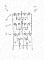
- FIG. 1 shows a schematic diagram of a first embodiment of an electrical according to the invention Circuit and the FIG. 2 shows a schematic diagram of a second embodiment of an electrical circuit according to the invention.
- a power converter 10 is shown, which is provided for converting a DC voltage into an AC voltage or vice versa.
- the power converter 10 is formed in three phases, but the power converter 10 could also have a different number of phases.
- NPC neutral point clamped
- the power converter 10 could have a different type of circuit configuration.
- the power converter 10 has a first series circuit 11, which consists of four IGBTs T1, T2, T3, T4 (IGBT insulated gate bipolar transistor) with in each case in parallel opposite freewheeling diodes D1, D2, D3, D4.
- IGBTs T1, T2, T3, T4 IGBT insulated gate bipolar transistor
- Two series-connected diodes D5, D6 are connected in parallel in opposite directions to the two middle IGBTs T2, T3.
- a resistor is connected in parallel with the two middle IGBTs T2, T3. This resistor may in particular be a so-called symmetry resistor Rsym.
- the series circuit 11 is connected to a terminal P (+) for a positive potential and to a terminal M (-) for a negative potential.
- the connection point of the two diodes D5, D6 is connected to a terminal N (0) for a Zero potential connected.
- the connection point of the two middle IGBTs T2, T3 forms a connection UR for an AC voltage.
- the power converter 10 has a second series circuit 12 and a third series circuit 13, which are constructed in the same way as the first series circuit 11.
- the three series circuits 11, 12, 13 are connected in parallel with each other.
- the connection point of the two central IGBTs there forms a connection UT for an AC voltage In the second series circuit 12, the connection point of the two central IGBTs there forms a connection US for an AC voltage and in the third series circuit 13, the connection point of the two central IGBTs there forms a connection UT for an AC voltage.
- a first capacitor Cd1 and between the N (0) terminal for a zero potential and the negative potential terminal M (-) is on second capacitor Cd2 arranged.
- the two capacitors Cd1, Cd2 form a so-called intermediate circuit.
- a first DC voltage U1 is applied to the first capacitor Cd1 and a second DC voltage U2 to the second capacitor Cd2.
- a voltage source is present which supplies energy to the capacitors Cd1, Cd2 and thus essentially generates or maintains the two direct voltages U1, U2.
- the voltage source may be, for example, a Power supply network, which is coupled via a rectifier with the two capacitors Cd1, Cd2.
- the IGBTs of the three series circuits 11, 12, 13 are controlled by a control unit that at the three terminals UR, US, UT a three-phase AC voltage Urst can be tapped.
- the IGBTs of the three series circuits 11, 12, 13 are continuously switched off and turned on by the control unit.
- the applied to the two capacitors Cd1, Cd2 DC voltages U1, U2 are implemented in this way by the power converter 10 in the AC voltage Urst.
- This AC voltage Urst can then apply, for example, a load, such as a drive motor or the like.
- this resistance is a so-called symmetry resistance Rsym.
- This symmetry resistor Rsym is intended to limit the voltage at the two middle IGBTs T2, T3.
- the two IGBTs T1, T2 block and the two IGBTs T3, T4 are turned on, then the sum of the two direct voltages U1, U2, the so-called intermediate circuit voltage, is applied to the two IGBTs T1, T2. Further, if, for example due to component tolerances or the like, the voltage drop across the IGBT T2 is substantially greater than the voltage drop across the IGBT T1, then it is possible - without the symmetrical resistance Rsym - to apply a voltage to the IGBT T2 which is a predetermined one Value, for example, exceeds half the DC link voltage.
- the voltage applied to the IGBT T2 can be exemplified be said half DC link voltage limited.
- the symmetry resistor Rsym and the IGBT T2 form a parallel circuit, and that by a corresponding selection of the resistance value of the symmetry resistor Rsym the voltage applied to this parallel circuit voltage can be limited to a desired value, for example, to half the DC link voltage.
- the resistor connected in parallel to the two middle IGBTs T3, T4 does not necessarily have to be the symmetry resistor Rsym explained above. It is also possible that the resistor is provided for another purpose or is provided only for the purpose explained below, ie only for discharging the two capacitors Cd1, Cd2 according to the methods described below.
- the two capacitors Cd1, Cd2 no longer supplied energy.
- the two capacitors Cd1, Cd2 are now discharged according to at least one of the following methods.
- the two IGBTs T1, T4 are turned on and the two IGBTs T2, T3 are blocked.
- the symmetry resistor Rsym is then connected in parallel to the two capacitors Cd1, Cd2. This allows a discharge current to flow via the two IGBTs T1, T4 and the symmetrical resistor Rsym.
- At least the IGBT T1 is turned on and the two IGETs T3, T4 are blocked.
- the symmetry resistor Rsym is then connected in parallel via the diode D6 to the first capacitor Cd1.
- a discharge current from the first capacitor Cd1 via the IGBT T1, the symmetry resistor Rsym and the diode D6 flow.
- At least the IGBT T4 is turned on and the two IGBTs T1, T2 are blocked.
- the symmetry resistor Rsym is then connected in parallel via the diode D5 to the second capacitor Cd2.
- a discharge current from the second capacitor Cd2 via the diode D5 the symmetry resistor Rsym and the IGBT T4 flow.
- the first capacitor Cd1 is discharged and then a predetermined period of time, the second capacitor Cd2 is discharged.
- first of all the first capacitor Cd1 may be fully discharged, and then the second capacitor Cd2 may be completely discharged as well.
- the discharge resistor may be a symmetry resistor already present in the converter or a resistor already existing in the converter for other reasons.
- FIG. 2 a power converter 20 is shown, which is provided for converting a DC voltage into an AC voltage or vice versa.
- the power converter 20 of the FIG. 2 corresponds largely to the power converter 10 of FIG. 1 , Matching components are therefore in the FIGS. 1 and 2 provided with matching reference numerals.
- Matching components are therefore in the FIGS. 1 and 2 provided with matching reference numerals.
- the structure and operation of the power converter 20 of the FIG. 2 is in this respect to the explanations to the power converter 10 of FIG. 1 directed.
- the two resistors R1, R2 of each phase may be symmetric resistors, but need not.
Landscapes
- Engineering & Computer Science (AREA)
- Power Engineering (AREA)
- Inverter Devices (AREA)
- Power Conversion In General (AREA)
Applications Claiming Priority (1)
| Application Number | Priority Date | Filing Date | Title |
|---|---|---|---|
| DE102012206409A DE102012206409A1 (de) | 2012-04-18 | 2012-04-18 | Verfahren zum Betreiben einer elektrischen Schaltung |
Publications (3)
| Publication Number | Publication Date |
|---|---|
| EP2654190A2 true EP2654190A2 (fr) | 2013-10-23 |
| EP2654190A3 EP2654190A3 (fr) | 2017-11-15 |
| EP2654190B1 EP2654190B1 (fr) | 2022-11-16 |
Family
ID=48095665
Family Applications (1)
| Application Number | Title | Priority Date | Filing Date |
|---|---|---|---|
| EP13163363.8A Revoked EP2654190B1 (fr) | 2012-04-18 | 2013-04-11 | Procédé de fonctionnement d'une commutation électrique |
Country Status (4)
| Country | Link |
|---|---|
| US (1) | US9276499B2 (fr) |
| EP (1) | EP2654190B1 (fr) |
| DE (1) | DE102012206409A1 (fr) |
| ES (1) | ES2933051T3 (fr) |
Cited By (4)
| Publication number | Priority date | Publication date | Assignee | Title |
|---|---|---|---|---|
| EP3373431A1 (fr) * | 2017-03-06 | 2018-09-12 | Siemens Aktiengesellschaft | Convertisseur d'énergie réglable destiné à convertir l'énergie électrique en énergie thermique |
| CN108736753A (zh) * | 2017-04-20 | 2018-11-02 | 丹佛斯电力电子有限公司 | 具有制动电阻连接的逆变器电路 |
| CN110460278A (zh) * | 2019-08-08 | 2019-11-15 | 华中科技大学 | 一种系留无人机的电机控制方法及存储介质和控制系统 |
| CN110971162A (zh) * | 2019-12-11 | 2020-04-07 | 浙江大学 | Npc三电平变流器-pmsm系统的改进模型预测转矩控制方法 |
Families Citing this family (6)
| Publication number | Priority date | Publication date | Assignee | Title |
|---|---|---|---|---|
| DE102012206409A1 (de) | 2012-04-18 | 2013-10-24 | Ge Energy Power Conversion Gmbh | Verfahren zum Betreiben einer elektrischen Schaltung |
| JP6080714B2 (ja) * | 2013-07-16 | 2017-02-15 | 東芝三菱電機産業システム株式会社 | 電力変換装置 |
| CN108123592B (zh) * | 2016-11-29 | 2020-11-10 | 台达电子企业管理(上海)有限公司 | 用于功率变流器母线电容的放电控制方法 |
| FR3060906B1 (fr) * | 2016-12-16 | 2019-05-24 | Ge Energy Power Conversion Technology Limited | Convertisseur continu-alternatif |
| CN109546879A (zh) * | 2018-12-06 | 2019-03-29 | 珠海格力电器股份有限公司 | 单相三电平混合箝位型逆变电路及具有其的逆变器 |
| EP4376286A4 (fr) * | 2021-11-19 | 2025-07-02 | Jingtsing Tech Ltd | Convertisseur de stockage d'énergie bidirectionnel |
Citations (2)
| Publication number | Priority date | Publication date | Assignee | Title |
|---|---|---|---|---|
| US5465202A (en) | 1990-11-30 | 1995-11-07 | Hitachi, Ltd. | Inverter apparatus provided with electric discharge control circuit of dc smoothing capacitor and method of controlling the same |
| DE19829856A1 (de) | 1998-07-02 | 2000-01-05 | Abb Research Ltd | Dreipunkt-Stromrichter und Verfahren zum Betrieb |
Family Cites Families (10)
| Publication number | Priority date | Publication date | Assignee | Title |
|---|---|---|---|---|
| DE19527178C1 (de) * | 1995-07-25 | 1996-11-07 | Siemens Ag | Rückspeiseschaltung für eine Entlastungsschaltung für einen Zweipunkt- bzw. Dreipunkt-Ventilzweig |
| DE19648948C1 (de) * | 1996-11-26 | 1998-03-05 | Siemens Ag | Wechselrichter mit Bremssteller |
| DE102004034948A1 (de) * | 2004-07-20 | 2006-03-16 | Abb Schweiz Ag | Spannungsanstiegsbegrenzte Umrichterschaltung |
| DE102004034945A1 (de) | 2004-07-20 | 2006-02-16 | Abb Schweiz Ag | Spannungsanstiegsbegrenzte Umrichterschaltung |
| DE102004034946A1 (de) | 2004-07-20 | 2006-02-16 | Abb Schweiz Ag | Spannungsanstiegsbegrenzte Umrichterschaltung |
| JP4600159B2 (ja) * | 2005-06-01 | 2010-12-15 | 三菱電機株式会社 | 3レベル電力変換装置 |
| WO2008075418A1 (fr) * | 2006-12-20 | 2008-06-26 | Mitsubishi Electric Corporation | Convertisseur de courant à trois états |
| CN201352765Y (zh) | 2008-11-18 | 2009-11-25 | Abb瑞士有限公司 | 功率电子积木模块 |
| RU2482599C1 (ru) * | 2009-05-13 | 2013-05-20 | Мицубиси Электрик Корпорейшн | Устройство преобразования энергии и способ управления напряжением на конденсаторе устройства преобразования энергии |
| DE102012206409A1 (de) | 2012-04-18 | 2013-10-24 | Ge Energy Power Conversion Gmbh | Verfahren zum Betreiben einer elektrischen Schaltung |
-
2012
- 2012-04-18 DE DE102012206409A patent/DE102012206409A1/de not_active Ceased
-
2013
- 2013-04-11 ES ES13163363T patent/ES2933051T3/es active Active
- 2013-04-11 EP EP13163363.8A patent/EP2654190B1/fr not_active Revoked
- 2013-04-18 US US13/865,535 patent/US9276499B2/en active Active
Patent Citations (2)
| Publication number | Priority date | Publication date | Assignee | Title |
|---|---|---|---|---|
| US5465202A (en) | 1990-11-30 | 1995-11-07 | Hitachi, Ltd. | Inverter apparatus provided with electric discharge control circuit of dc smoothing capacitor and method of controlling the same |
| DE19829856A1 (de) | 1998-07-02 | 2000-01-05 | Abb Research Ltd | Dreipunkt-Stromrichter und Verfahren zum Betrieb |
Cited By (6)
| Publication number | Priority date | Publication date | Assignee | Title |
|---|---|---|---|---|
| EP3373431A1 (fr) * | 2017-03-06 | 2018-09-12 | Siemens Aktiengesellschaft | Convertisseur d'énergie réglable destiné à convertir l'énergie électrique en énergie thermique |
| CN108736753A (zh) * | 2017-04-20 | 2018-11-02 | 丹佛斯电力电子有限公司 | 具有制动电阻连接的逆变器电路 |
| US11323044B2 (en) | 2017-04-20 | 2022-05-03 | Danfoss Power Electronics A/S | Three-level inverter and a three-level brake chopper |
| CN110460278A (zh) * | 2019-08-08 | 2019-11-15 | 华中科技大学 | 一种系留无人机的电机控制方法及存储介质和控制系统 |
| CN110971162A (zh) * | 2019-12-11 | 2020-04-07 | 浙江大学 | Npc三电平变流器-pmsm系统的改进模型预测转矩控制方法 |
| CN110971162B (zh) * | 2019-12-11 | 2021-04-06 | 浙江大学 | Npc三电平变流器-pmsm系统的模型预测转矩控制方法 |
Also Published As
| Publication number | Publication date |
|---|---|
| EP2654190A3 (fr) | 2017-11-15 |
| US9276499B2 (en) | 2016-03-01 |
| EP2654190B1 (fr) | 2022-11-16 |
| DE102012206409A1 (de) | 2013-10-24 |
| US20130301325A1 (en) | 2013-11-14 |
| ES2933051T3 (es) | 2023-01-31 |
Similar Documents
| Publication | Publication Date | Title |
|---|---|---|
| EP2654190B1 (fr) | Procédé de fonctionnement d'une commutation électrique | |
| EP2596980B1 (fr) | Convertisseur de courant à plusieurs points avec hacheur de freinage | |
| DE102008036811B4 (de) | Redundanzsteuerverfahren eines mehrphasigen Stromrichters mit verteilten Energiespeichern | |
| DE102020200794B4 (de) | Lade- und Heizschaltung | |
| EP2541746B1 (fr) | Procédé de déchartge d'un condensateur de circuit intermédiaire d'un convertisseur et circuit correspondant | |
| DE102016123678A1 (de) | Anordnung und Verfahren zur Erzeugung einer negativen Spannung für einen High-Side-Schalter in einem Wechselrichter | |
| DE19961382A1 (de) | Elektrische Schaltung, insbesondere für einen Mittelspannungsstromrichter | |
| DE102019105196B4 (de) | Verfahren zur Strombegrenzung bei transienten Spannungsänderungen an einem Wechselstromausgang eines Multilevel-Wechselrichters und Multilevel-Wechselrichter | |
| DE102015013875A1 (de) | Wechseleinrichter für eine elektrische Maschine, elektrische Antriebseinrichtung für ein Kraftfahrzeug sowie Verfahren zum Betreiben eines Wechselrichters | |
| EP3251194B1 (fr) | Ensemble d'accumulation d'énergie | |
| DE102009039195A1 (de) | N-stufiger elektrischer Stromrichter | |
| WO2013023914A1 (fr) | Dispositif onduleur | |
| DE102015105889A1 (de) | Schaltmodul und Umrichter mit wenigstens einem Schaltmodul | |
| DE102011087153A1 (de) | Mehrpunkt-Stromrichter mit Bremschopper | |
| DE102017203233A1 (de) | Modularer Wechselrichter | |
| DE102018212523B4 (de) | Fahrzeugseitige Ladeschaltung | |
| DE102020203994A1 (de) | Verfahren zum Ansteuern von Schaltelementen eines modularen Multilevelstromrichters | |
| DE102013109714A1 (de) | Verfahren zum Betreiben einer elektrischen Schaltung sowie elektrische Schaltung | |
| EP3218980B1 (fr) | Procédé de transmission à courant continu | |
| EP2184844A1 (fr) | Onduleur électrique | |
| EP2928055B1 (fr) | Convertisseur de courant modulaire et procédé de production d'une tension de sortie sinusoïdale à harmoniques réduites | |
| DE102013220864B3 (de) | Stromrichter | |
| EP3373431A1 (fr) | Convertisseur d'énergie réglable destiné à convertir l'énergie électrique en énergie thermique | |
| DE102013207894A1 (de) | Elektrische Schaltung | |
| EP3883116B1 (fr) | Véhicule, en particulier véhicule ferroviaire |
Legal Events
| Date | Code | Title | Description |
|---|---|---|---|
| PUAI | Public reference made under article 153(3) epc to a published international application that has entered the european phase |
Free format text: ORIGINAL CODE: 0009012 |
|
| AK | Designated contracting states |
Kind code of ref document: A2 Designated state(s): AL AT BE BG CH CY CZ DE DK EE ES FI FR GB GR HR HU IE IS IT LI LT LU LV MC MK MT NL NO PL PT RO RS SE SI SK SM TR |
|
| AX | Request for extension of the european patent |
Extension state: BA ME |
|
| PUAL | Search report despatched |
Free format text: ORIGINAL CODE: 0009013 |
|
| AK | Designated contracting states |
Kind code of ref document: A3 Designated state(s): AL AT BE BG CH CY CZ DE DK EE ES FI FR GB GR HR HU IE IS IT LI LT LU LV MC MK MT NL NO PL PT RO RS SE SI SK SM TR |
|
| AX | Request for extension of the european patent |
Extension state: BA ME |
|
| RIC1 | Information provided on ipc code assigned before grant |
Ipc: H02M 7/487 20070101AFI20171011BHEP Ipc: H02P 27/08 20060101ALI20171011BHEP Ipc: H02M 7/797 20060101ALI20171011BHEP |
|
| STAA | Information on the status of an ep patent application or granted ep patent |
Free format text: STATUS: REQUEST FOR EXAMINATION WAS MADE |
|
| 17P | Request for examination filed |
Effective date: 20180515 |
|
| RBV | Designated contracting states (corrected) |
Designated state(s): AL AT BE BG CH CY CZ DE DK EE ES FI FR GB GR HR HU IE IS IT LI LT LU LV MC MK MT NL NO PL PT RO RS SE SI SK SM TR |
|
| STAA | Information on the status of an ep patent application or granted ep patent |
Free format text: STATUS: EXAMINATION IS IN PROGRESS |
|
| 17Q | First examination report despatched |
Effective date: 20201203 |
|
| GRAP | Despatch of communication of intention to grant a patent |
Free format text: ORIGINAL CODE: EPIDOSNIGR1 |
|
| STAA | Information on the status of an ep patent application or granted ep patent |
Free format text: STATUS: GRANT OF PATENT IS INTENDED |
|
| INTG | Intention to grant announced |
Effective date: 20220602 |
|
| GRAS | Grant fee paid |
Free format text: ORIGINAL CODE: EPIDOSNIGR3 |
|
| GRAA | (expected) grant |
Free format text: ORIGINAL CODE: 0009210 |
|
| STAA | Information on the status of an ep patent application or granted ep patent |
Free format text: STATUS: THE PATENT HAS BEEN GRANTED |
|
| AK | Designated contracting states |
Kind code of ref document: B1 Designated state(s): AL AT BE BG CH CY CZ DE DK EE ES FI FR GB GR HR HU IE IS IT LI LT LU LV MC MK MT NL NO PL PT RO RS SE SI SK SM TR |
|
| REG | Reference to a national code |
Ref country code: GB Ref legal event code: FG4D Free format text: NOT ENGLISH |
|
| REG | Reference to a national code |
Ref country code: CH Ref legal event code: EP |
|
| REG | Reference to a national code |
Ref country code: IE Ref legal event code: FG4D Free format text: LANGUAGE OF EP DOCUMENT: GERMAN |
|
| REG | Reference to a national code |
Ref country code: DE Ref legal event code: R096 Ref document number: 502013016286 Country of ref document: DE |
|
| REG | Reference to a national code |
Ref country code: AT Ref legal event code: REF Ref document number: 1532382 Country of ref document: AT Kind code of ref document: T Effective date: 20221215 |
|
| REG | Reference to a national code |
Ref country code: SE Ref legal event code: TRGR |
|
| REG | Reference to a national code |
Ref country code: ES Ref legal event code: FG2A Ref document number: 2933051 Country of ref document: ES Kind code of ref document: T3 Effective date: 20230131 |
|
| REG | Reference to a national code |
Ref country code: LT Ref legal event code: MG9D |
|
| REG | Reference to a national code |
Ref country code: NL Ref legal event code: MP Effective date: 20221116 |
|
| PG25 | Lapsed in a contracting state [announced via postgrant information from national office to epo] |
Ref country code: PT Free format text: LAPSE BECAUSE OF FAILURE TO SUBMIT A TRANSLATION OF THE DESCRIPTION OR TO PAY THE FEE WITHIN THE PRESCRIBED TIME-LIMIT Effective date: 20230316 Ref country code: NO Free format text: LAPSE BECAUSE OF FAILURE TO SUBMIT A TRANSLATION OF THE DESCRIPTION OR TO PAY THE FEE WITHIN THE PRESCRIBED TIME-LIMIT Effective date: 20230216 Ref country code: LT Free format text: LAPSE BECAUSE OF FAILURE TO SUBMIT A TRANSLATION OF THE DESCRIPTION OR TO PAY THE FEE WITHIN THE PRESCRIBED TIME-LIMIT Effective date: 20221116 Ref country code: FI Free format text: LAPSE BECAUSE OF FAILURE TO SUBMIT A TRANSLATION OF THE DESCRIPTION OR TO PAY THE FEE WITHIN THE PRESCRIBED TIME-LIMIT Effective date: 20221116 |
|
| PGFP | Annual fee paid to national office [announced via postgrant information from national office to epo] |
Ref country code: FR Payment date: 20230321 Year of fee payment: 11 |
|
| PG25 | Lapsed in a contracting state [announced via postgrant information from national office to epo] |
Ref country code: RS Free format text: LAPSE BECAUSE OF FAILURE TO SUBMIT A TRANSLATION OF THE DESCRIPTION OR TO PAY THE FEE WITHIN THE PRESCRIBED TIME-LIMIT Effective date: 20221116 Ref country code: PL Free format text: LAPSE BECAUSE OF FAILURE TO SUBMIT A TRANSLATION OF THE DESCRIPTION OR TO PAY THE FEE WITHIN THE PRESCRIBED TIME-LIMIT Effective date: 20221116 Ref country code: LV Free format text: LAPSE BECAUSE OF FAILURE TO SUBMIT A TRANSLATION OF THE DESCRIPTION OR TO PAY THE FEE WITHIN THE PRESCRIBED TIME-LIMIT Effective date: 20221116 Ref country code: IS Free format text: LAPSE BECAUSE OF FAILURE TO SUBMIT A TRANSLATION OF THE DESCRIPTION OR TO PAY THE FEE WITHIN THE PRESCRIBED TIME-LIMIT Effective date: 20230316 Ref country code: HR Free format text: LAPSE BECAUSE OF FAILURE TO SUBMIT A TRANSLATION OF THE DESCRIPTION OR TO PAY THE FEE WITHIN THE PRESCRIBED TIME-LIMIT Effective date: 20221116 Ref country code: GR Free format text: LAPSE BECAUSE OF FAILURE TO SUBMIT A TRANSLATION OF THE DESCRIPTION OR TO PAY THE FEE WITHIN THE PRESCRIBED TIME-LIMIT Effective date: 20230217 |
|
| PGFP | Annual fee paid to national office [announced via postgrant information from national office to epo] |
Ref country code: SE Payment date: 20230327 Year of fee payment: 11 Ref country code: IT Payment date: 20230322 Year of fee payment: 11 |
|
| PG25 | Lapsed in a contracting state [announced via postgrant information from national office to epo] |
Ref country code: NL Free format text: LAPSE BECAUSE OF FAILURE TO SUBMIT A TRANSLATION OF THE DESCRIPTION OR TO PAY THE FEE WITHIN THE PRESCRIBED TIME-LIMIT Effective date: 20221116 |
|
| P01 | Opt-out of the competence of the unified patent court (upc) registered |
Effective date: 20230530 |
|
| PG25 | Lapsed in a contracting state [announced via postgrant information from national office to epo] |
Ref country code: SM Free format text: LAPSE BECAUSE OF FAILURE TO SUBMIT A TRANSLATION OF THE DESCRIPTION OR TO PAY THE FEE WITHIN THE PRESCRIBED TIME-LIMIT Effective date: 20221116 Ref country code: RO Free format text: LAPSE BECAUSE OF FAILURE TO SUBMIT A TRANSLATION OF THE DESCRIPTION OR TO PAY THE FEE WITHIN THE PRESCRIBED TIME-LIMIT Effective date: 20221116 Ref country code: EE Free format text: LAPSE BECAUSE OF FAILURE TO SUBMIT A TRANSLATION OF THE DESCRIPTION OR TO PAY THE FEE WITHIN THE PRESCRIBED TIME-LIMIT Effective date: 20221116 Ref country code: DK Free format text: LAPSE BECAUSE OF FAILURE TO SUBMIT A TRANSLATION OF THE DESCRIPTION OR TO PAY THE FEE WITHIN THE PRESCRIBED TIME-LIMIT Effective date: 20221116 Ref country code: CZ Free format text: LAPSE BECAUSE OF FAILURE TO SUBMIT A TRANSLATION OF THE DESCRIPTION OR TO PAY THE FEE WITHIN THE PRESCRIBED TIME-LIMIT Effective date: 20221116 |
|
| PGFP | Annual fee paid to national office [announced via postgrant information from national office to epo] |
Ref country code: ES Payment date: 20230502 Year of fee payment: 11 Ref country code: DE Payment date: 20230321 Year of fee payment: 11 Ref country code: CH Payment date: 20230502 Year of fee payment: 11 |
|
| REG | Reference to a national code |
Ref country code: DE Ref legal event code: R026 Ref document number: 502013016286 Country of ref document: DE |
|
| PLBI | Opposition filed |
Free format text: ORIGINAL CODE: 0009260 |
|
| PLAX | Notice of opposition and request to file observation + time limit sent |
Free format text: ORIGINAL CODE: EPIDOSNOBS2 |
|
| PG25 | Lapsed in a contracting state [announced via postgrant information from national office to epo] |
Ref country code: SK Free format text: LAPSE BECAUSE OF FAILURE TO SUBMIT A TRANSLATION OF THE DESCRIPTION OR TO PAY THE FEE WITHIN THE PRESCRIBED TIME-LIMIT Effective date: 20221116 Ref country code: AL Free format text: LAPSE BECAUSE OF FAILURE TO SUBMIT A TRANSLATION OF THE DESCRIPTION OR TO PAY THE FEE WITHIN THE PRESCRIBED TIME-LIMIT Effective date: 20221116 |
|
| 26 | Opposition filed |
Opponent name: HITACHI ENERGY SWITZERLAND AG Effective date: 20230816 |
|
| PG25 | Lapsed in a contracting state [announced via postgrant information from national office to epo] |
Ref country code: SI Free format text: LAPSE BECAUSE OF FAILURE TO SUBMIT A TRANSLATION OF THE DESCRIPTION OR TO PAY THE FEE WITHIN THE PRESCRIBED TIME-LIMIT Effective date: 20221116 |
|
| PLAB | Opposition data, opponent's data or that of the opponent's representative modified |
Free format text: ORIGINAL CODE: 0009299OPPO |
|
| PLBB | Reply of patent proprietor to notice(s) of opposition received |
Free format text: ORIGINAL CODE: EPIDOSNOBS3 |
|
| GBPC | Gb: european patent ceased through non-payment of renewal fee |
Effective date: 20230411 |
|
| PG25 | Lapsed in a contracting state [announced via postgrant information from national office to epo] |
Ref country code: LU Free format text: LAPSE BECAUSE OF NON-PAYMENT OF DUE FEES Effective date: 20230411 |
|
| R26 | Opposition filed (corrected) |
Opponent name: HITACHI ENERGY LTD Effective date: 20230816 |
|
| REG | Reference to a national code |
Ref country code: BE Ref legal event code: MM Effective date: 20230430 |
|
| PG25 | Lapsed in a contracting state [announced via postgrant information from national office to epo] |
Ref country code: MC Free format text: LAPSE BECAUSE OF FAILURE TO SUBMIT A TRANSLATION OF THE DESCRIPTION OR TO PAY THE FEE WITHIN THE PRESCRIBED TIME-LIMIT Effective date: 20221116 |
|
| PG25 | Lapsed in a contracting state [announced via postgrant information from national office to epo] |
Ref country code: GB Free format text: LAPSE BECAUSE OF NON-PAYMENT OF DUE FEES Effective date: 20230411 |
|
| PG25 | Lapsed in a contracting state [announced via postgrant information from national office to epo] |
Ref country code: MC Free format text: LAPSE BECAUSE OF FAILURE TO SUBMIT A TRANSLATION OF THE DESCRIPTION OR TO PAY THE FEE WITHIN THE PRESCRIBED TIME-LIMIT Effective date: 20221116 Ref country code: GB Free format text: LAPSE BECAUSE OF NON-PAYMENT OF DUE FEES Effective date: 20230411 |
|
| REG | Reference to a national code |
Ref country code: IE Ref legal event code: MM4A |
|
| PG25 | Lapsed in a contracting state [announced via postgrant information from national office to epo] |
Ref country code: BE Free format text: LAPSE BECAUSE OF NON-PAYMENT OF DUE FEES Effective date: 20230430 |
|
| PG25 | Lapsed in a contracting state [announced via postgrant information from national office to epo] |
Ref country code: IE Free format text: LAPSE BECAUSE OF NON-PAYMENT OF DUE FEES Effective date: 20230411 |
|
| RDAF | Communication despatched that patent is revoked |
Free format text: ORIGINAL CODE: EPIDOSNREV1 |
|
| REG | Reference to a national code |
Ref country code: DE Ref legal event code: R103 Ref document number: 502013016286 Country of ref document: DE Ref country code: DE Ref legal event code: R064 Ref document number: 502013016286 Country of ref document: DE |
|
| PG25 | Lapsed in a contracting state [announced via postgrant information from national office to epo] |
Ref country code: IE Free format text: LAPSE BECAUSE OF NON-PAYMENT OF DUE FEES Effective date: 20230411 |
|
| REG | Reference to a national code |
Ref country code: AT Ref legal event code: MM01 Ref document number: 1532382 Country of ref document: AT Kind code of ref document: T Effective date: 20230411 |
|
| PG25 | Lapsed in a contracting state [announced via postgrant information from national office to epo] |
Ref country code: AT Free format text: LAPSE BECAUSE OF NON-PAYMENT OF DUE FEES Effective date: 20230411 |
|
| RDAG | Patent revoked |
Free format text: ORIGINAL CODE: 0009271 |
|
| STAA | Information on the status of an ep patent application or granted ep patent |
Free format text: STATUS: PATENT REVOKED |
|
| PG25 | Lapsed in a contracting state [announced via postgrant information from national office to epo] |
Ref country code: AT Free format text: LAPSE BECAUSE OF NON-PAYMENT OF DUE FEES Effective date: 20230411 |
|
| REG | Reference to a national code |
Ref country code: CH Ref legal event code: PL |
|
| 27W | Patent revoked |
Effective date: 20240425 |
|
| PG25 | Lapsed in a contracting state [announced via postgrant information from national office to epo] |
Ref country code: BG Free format text: LAPSE BECAUSE OF FAILURE TO SUBMIT A TRANSLATION OF THE DESCRIPTION OR TO PAY THE FEE WITHIN THE PRESCRIBED TIME-LIMIT Effective date: 20221116 |
|
| REG | Reference to a national code |
Ref country code: AT Ref legal event code: MA03 Ref document number: 1532382 Country of ref document: AT Kind code of ref document: T Effective date: 20240425 |
|
| PG25 | Lapsed in a contracting state [announced via postgrant information from national office to epo] |
Ref country code: BG Free format text: LAPSE BECAUSE OF FAILURE TO SUBMIT A TRANSLATION OF THE DESCRIPTION OR TO PAY THE FEE WITHIN THE PRESCRIBED TIME-LIMIT Effective date: 20221116 |
|
| REG | Reference to a national code |
Ref country code: SE Ref legal event code: ECNC |
|
| PG25 | Lapsed in a contracting state [announced via postgrant information from national office to epo] |
Ref country code: CY Free format text: LAPSE BECAUSE OF FAILURE TO SUBMIT A TRANSLATION OF THE DESCRIPTION OR TO PAY THE FEE WITHIN THE PRESCRIBED TIME-LIMIT; INVALID AB INITIO Effective date: 20130411 |
|
| PG25 | Lapsed in a contracting state [announced via postgrant information from national office to epo] |
Ref country code: HU Free format text: LAPSE BECAUSE OF FAILURE TO SUBMIT A TRANSLATION OF THE DESCRIPTION OR TO PAY THE FEE WITHIN THE PRESCRIBED TIME-LIMIT; INVALID AB INITIO Effective date: 20130411 |
|
| PG25 | Lapsed in a contracting state [announced via postgrant information from national office to epo] |
Ref country code: TR Free format text: LAPSE BECAUSE OF FAILURE TO SUBMIT A TRANSLATION OF THE DESCRIPTION OR TO PAY THE FEE WITHIN THE PRESCRIBED TIME-LIMIT Effective date: 20221116 |