EP2656412B1 - Organisches halbleiterbauelement mit dotierter lochleiterschicht - Google Patents
Organisches halbleiterbauelement mit dotierter lochleiterschicht Download PDFInfo
- Publication number
- EP2656412B1 EP2656412B1 EP12700039.6A EP12700039A EP2656412B1 EP 2656412 B1 EP2656412 B1 EP 2656412B1 EP 12700039 A EP12700039 A EP 12700039A EP 2656412 B1 EP2656412 B1 EP 2656412B1
- Authority
- EP
- European Patent Office
- Prior art keywords
- hole conductor
- conductor layer
- tfms
- bis
- doping
- Prior art date
- Legal status (The legal status is an assumption and is not a legal conclusion. Google has not performed a legal analysis and makes no representation as to the accuracy of the status listed.)
- Active
Links
Images






Classifications
-
- H—ELECTRICITY
- H10—SEMICONDUCTOR DEVICES; ELECTRIC SOLID-STATE DEVICES NOT OTHERWISE PROVIDED FOR
- H10K—ORGANIC ELECTRIC SOLID-STATE DEVICES
- H10K71/00—Manufacture or treatment specially adapted for the organic devices covered by this subclass
- H10K71/30—Doping active layers, e.g. electron transporting layers
-
- H—ELECTRICITY
- H10—SEMICONDUCTOR DEVICES; ELECTRIC SOLID-STATE DEVICES NOT OTHERWISE PROVIDED FOR
- H10K—ORGANIC ELECTRIC SOLID-STATE DEVICES
- H10K50/00—Organic light-emitting devices
- H10K50/10—OLEDs or polymer light-emitting diodes [PLED]
- H10K50/14—Carrier transporting layers
- H10K50/15—Hole transporting layers
- H10K50/155—Hole transporting layers comprising dopants
-
- H—ELECTRICITY
- H10—SEMICONDUCTOR DEVICES; ELECTRIC SOLID-STATE DEVICES NOT OTHERWISE PROVIDED FOR
- H10K—ORGANIC ELECTRIC SOLID-STATE DEVICES
- H10K50/00—Organic light-emitting devices
- H10K50/10—OLEDs or polymer light-emitting diodes [PLED]
- H10K50/14—Carrier transporting layers
- H10K50/15—Hole transporting layers
- H10K50/156—Hole transporting layers comprising a multilayered structure
-
- H—ELECTRICITY
- H10—SEMICONDUCTOR DEVICES; ELECTRIC SOLID-STATE DEVICES NOT OTHERWISE PROVIDED FOR
- H10K—ORGANIC ELECTRIC SOLID-STATE DEVICES
- H10K71/00—Manufacture or treatment specially adapted for the organic devices covered by this subclass
-
- H—ELECTRICITY
- H10—SEMICONDUCTOR DEVICES; ELECTRIC SOLID-STATE DEVICES NOT OTHERWISE PROVIDED FOR
- H10K—ORGANIC ELECTRIC SOLID-STATE DEVICES
- H10K85/00—Organic materials used in the body or electrodes of devices covered by this subclass
- H10K85/60—Organic compounds having low molecular weight
- H10K85/611—Charge transfer complexes
-
- H—ELECTRICITY
- H10—SEMICONDUCTOR DEVICES; ELECTRIC SOLID-STATE DEVICES NOT OTHERWISE PROVIDED FOR
- H10K—ORGANIC ELECTRIC SOLID-STATE DEVICES
- H10K50/00—Organic light-emitting devices
- H10K50/10—OLEDs or polymer light-emitting diodes [PLED]
- H10K50/17—Carrier injection layers
-
- H—ELECTRICITY
- H10—SEMICONDUCTOR DEVICES; ELECTRIC SOLID-STATE DEVICES NOT OTHERWISE PROVIDED FOR
- H10K—ORGANIC ELECTRIC SOLID-STATE DEVICES
- H10K50/00—Organic light-emitting devices
- H10K50/10—OLEDs or polymer light-emitting diodes [PLED]
- H10K50/18—Carrier blocking layers
-
- H—ELECTRICITY
- H10—SEMICONDUCTOR DEVICES; ELECTRIC SOLID-STATE DEVICES NOT OTHERWISE PROVIDED FOR
- H10K—ORGANIC ELECTRIC SOLID-STATE DEVICES
- H10K71/00—Manufacture or treatment specially adapted for the organic devices covered by this subclass
- H10K71/10—Deposition of organic active material
- H10K71/12—Deposition of organic active material using liquid deposition, e.g. spin coating
-
- H—ELECTRICITY
- H10—SEMICONDUCTOR DEVICES; ELECTRIC SOLID-STATE DEVICES NOT OTHERWISE PROVIDED FOR
- H10K—ORGANIC ELECTRIC SOLID-STATE DEVICES
- H10K71/00—Manufacture or treatment specially adapted for the organic devices covered by this subclass
- H10K71/10—Deposition of organic active material
- H10K71/16—Deposition of organic active material using physical vapour deposition [PVD], e.g. vacuum deposition or sputtering
-
- H—ELECTRICITY
- H10—SEMICONDUCTOR DEVICES; ELECTRIC SOLID-STATE DEVICES NOT OTHERWISE PROVIDED FOR
- H10K—ORGANIC ELECTRIC SOLID-STATE DEVICES
- H10K85/00—Organic materials used in the body or electrodes of devices covered by this subclass
- H10K85/60—Organic compounds having low molecular weight
- H10K85/631—Amine compounds having at least two aryl rest on at least one amine-nitrogen atom, e.g. triphenylamine
- H10K85/633—Amine compounds having at least two aryl rest on at least one amine-nitrogen atom, e.g. triphenylamine comprising polycyclic condensed aromatic hydrocarbons as substituents on the nitrogen atom
Definitions
- the present invention relates to organic semiconductor components and their manufacture.
- An organic light-emitting diode is only one example from the prior art in which doping is used to increase the conductivity of charge transport layers and so-called “charge generation layers”.
- the problem of doping also arises in organic field effect transistors, solar cells or photodetectors, for example for injection layers to reduce the contact resistance, for example at source and drain electrodes or electrodes in general.
- the dopants are limited to one deposition method and can accordingly be processed exclusively from the gas phase or exclusively from the liquid phase. Accordingly, these dopant classes are also limited to one material class each for the semiconductor matrix. I.e. a dopant that can only be deposited from the liquid phase can only be introduced into a polymer matrix. A dopant that can only be deposited from the gas phase can only be introduced into a "small molecule matrix". In terms of suitability for deposition from the gas phase, there is also the fact that the dopant must be able to be heated to a certain temperature without it being decomposed. Only if the dopant is suitable to form a doped hole conductor layer in a condensation reaction together with the matrix material, it should be taken into account for use in component manufacture.
- the primary aim is to further improve their doping effect and thereby further increase the conductivity of organic semiconductor layers.
- compositions for use in hole conductor layers or hole injection layers methods of making these compositions, and devices that can be made with these compositions.
- Organic light-emitting diodes can be produced.
- the compositions consist of at least one conductive conjugated polymer, at least one semiconducting matrix component that is different from the conductive conjugated polymer, and optionally a dopant, the compositions being substantially free of an insulating matrix component.
- the device according to the invention is a semiconductor component with at least one organic hole conductor layer.
- This hole conductor layer is p-doped with a super acid salt.
- the super acid salt contains silver (I) trifluoromethanesulfonate (Ag (I) TFMS) and / or copper (II) trifluoromethanesulfonate (Cu (II) TFMS).
- the substance class of the super acid salts surprisingly turns out to be very good p-dopant in hole conductor layers.
- the advantage of the invention is a greatly increased conductivity of the hole conductor layer by introducing the doping at very low concentrations of the dopant.
- the semiconductor component has a hole conductor layer which has a specific conductivity of at least 2.5 ⁇ 10 -5 S / m, and the doping concentration is at most 20% by volume.
- the super acid salts have the advantage of achieving high conductivities at low concentrations in the hole-conducting matrix.
- the semiconductor component has a hole conductor layer which has p-doping with a super acid salt, the super acid salt having silver (I) trifluoromethanesulfonate (Ag (I) TFMS) and the absorption capacity of the hole conductor layer in the wavelength range between 400 nm and 700 nm is essentially not increased by the p-doping with the super acid salt.
- Substantially not increased means that the color impression remains unchanged for the human eye, whether or not doping has been introduced into the matrix.
- This has the advantage that the doping does not change the color impression, in particular when the component is switched off.
- the color impression is particularly important in the case of organic light-emitting diodes.
- the doping according to the invention is therefore particularly preferred for use in organic light-emitting diodes.
- the silver (I) trifluoromethanesulfonate has the advantage of increasing the conductivity to over 7 ⁇ 10 -5 S / m, with a doping concentration of 10% or less. This corresponds to an increase in the current density at 1V component voltage and 200 nm layer thickness by 6 orders of magnitude.
- the particular advantage of silver (I) trifluoromethanesulfonate is its low absorption in the visible wavelength range, which causes the hole conductor layer doped in this way to appear neutral in color to the human eye.
- copper (II) trifluoromethanesulfonate is particularly characterized by the fact that it can increase the conductivity of the hole conductor layer to over 5 ⁇ 10 -2 S / m at a concentration of 10%.
- an organic hole conductor layer which has p-doping with a super acid salt is deposited in one step, the super acid salt having a salt of a super acid, and the super acid being an acid with an acid constant value pKs smaller than that of Sulfuric acid is.
- a matrix material is deposited together with the super acid salt from the gas phase in a common step, the doping concentration of the hole conductor layer being adjusted via the evaporation rates of the super acid salt and the matrix material in a co-evaporation.
- the volume concentration set via the evaporation rates of the p-dopant in the matrix material can deviate from the actual volume concentration in the completely deposited hole conductor layer.
- the inventive p-doping with super acid salts thus has the advantage of being able to adapt the dopant very well to the matrix material through the choice of cation and acid anion.
- the optical properties for the use of the p-dopant in organic light-emitting diodes can be greatly improved by this new class of materials for p-doping.
- a high conductivity is achieved even with low doping concentrations.
- the inventive p-doping can be used to achieve a compromise between optical and electrical properties.
- the visual appearance of the doped layers is also important for the quality of an organic semiconductor component, especially for display applications or lighting purposes.
- Trifluoromethylsulfonic acid (HSO 3 CF 3 ) is a particularly suitable representative of these.
- the cations listed are also suitable for forming salts with anions of other superacids, which salts can be used as p-dopants.
- the triflates of the transition metals, in particular of silver and copper, are very particularly preferred.
- the super acid salts formed in this way are volatile and can form a doped hole conductor layer together with a hole conductor in particular in the context of a cocondensation reaction.
- the super acid salts are also very stable, especially in anhydrous form, and can even be heated to well over 400 ° C.
- Copper (I) trifluoromethanesulfonate is only suitable for solution processing as it cannot be evaporated without being decomposed.
- copper (I) trifluoromethanesulfonate can be processed, for example in the solvate with benzene (C 6 H 6 ), toluene (C 7 H 8 ) or acetonitrile (C 2 H 3 N): benzene toluene Acetonitrile
- a major advantage of the invention is the cost savings.
- the use of salts of super acids as p-dopants for hole conductor layers in OLEDs has the advantage of extremely low costs in addition to the high doping capacity.
- the costs of the p-dopants currently used are between 2000 and 7000 € / g, depending on the amount purchased.
- Ag (I) CF 3 SO 3 and Cu (II) [CF 3 SO 3 ] 2 are less than 10 € / g in the normal fine chemicals trade.
- many representatives of this class are commercially available or at least their manufacturing processes are known, well-developed and inexpensive.
- Organic hole conductors are generally, but not exclusively, derivatives of triarylamines.
- monomolecular hole transport materials can also be deposited from the liquid phase or added to the polymeric materials mentioned below in solution. If low-molecular and polymeric materials are mixed, the film-forming properties can be influenced and improved via the mixing ratio (between 0 and 100%).
- Polymer hole transporters which are primarily deposited from the liquid phase, are in particular but not restrictive: - PEDOT (poly (3,4 ethylenedioxythiophene)) - PVK (poly (9-vinylcarbazole)) - PTPD (poly (N, N'-bis (4-butylphenyl) -N, N'-bis (phenyl) -benzidine)) - P3HT (poly (3-hexylthiophenes)) - PANI (polyaniline)
- Another particular advantage of the invention is that the material class of super acid salts suitable for p-doping is deposited with the hole conductor matrix from the same gas phase.
- the Figure 1 shows schematically the structure of an organic semiconductor component 10. This structure is used in particular for organic light-emitting diodes.
- a lower electrode 12 and an upper electrode 13 and a plurality of organic semiconductor layers in between are placed on a glass substrate 11 deposited.
- a cross-section through the horizontally arranged layers is shown.
- the component voltage U d can be applied to the lower 12 and upper 13 electrodes.
- the upper electrode 13 is the cathode of the light-emitting diode and the lower electrode 12 is the anode of the light-emitting diode.
- the light decoupling L occurs through the glass substrate 11.
- the anode is transparent, in particular made of indium tin oxide (ITO).
- the hole-conducting layers 20 initially adjoin the anode. These can be designed for different focus functions.
- the first layer 21 on the anode represents a hole injection layer.
- the hole conductor layer 22 connected to it is a hole transport layer and the third hole conductor layer 23 connected to it functions as an electron blocking layer in order to prevent the electrons coming from the cathode side to penetrate the hole guiding area.
- the electron transport area follows.
- This can also comprise a plurality of electron conducting layers 40.
- the cathode is followed by a first electron conduction layer 43, which acts as an electron injection layer.
- a second electron transport layer 42 is subsequently shown and a third electron transport layer 41 can in turn be used as a hole-blocking layer.
- the emission area is located between the electron transport area and the hole transport area. This in turn can consist of several layers.
- the emission area has three emission layers 30 of different colors: a red emission layer 31 adjoins the hole transport area, followed by a green emission layer 32 and a blue emission layer 33 adjoins the electron transport area.
- the layer according to the invention can also be installed in a charge generation layer.
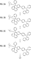
- the doping can be carried out by coordinating one or two hole conductor molecules, such as, for example, NPB, in the axial positions of the Cu (II) complex, as shown schematically in FIG Figure 2 shown.
- the Figure 2 shows schematically the various representations of the mesomeric boundary structures of the complex:
- the dopant in this example a Cu (II) complex
- NPB hole-conducting matrix
- state B there is a purely formal charge transfer in the form of an electron from the NPB molecule to the Cu (II) complex, ie a formal / partial charge transfer of a positive charge to the NPB molecule.
- the copper atom is then only monovalent.
- state C it is shown that the positive charge, also known as a hole, can move over the NPB molecule and in state D can also be transferred to a second neighboring NPB molecule, which ultimately corresponds to hopping transport in organic semiconductors.
- This coordination can be so strong that even materials that are preferentially electron-conducting in the non-coordinated state are reversed in polarity and become hole conductors.
- Cu (II) trifluoromethanesulfonate can be purified by means of zone sublimation at a base pressure of 2 ⁇ 10 -4 Pa (2 ⁇ 10 -6 mbar).
- the material can in particular be sublimed twice, whereby existing residues and impurities are removed.
- sublimation steps can be carried out at different temperatures.
- HTM-014 a 200 nm thick doped hole conductor layer with the hole conductor matrix material HTM-014 was deposited on an ITO electrode (indium-doped tin oxide) by thermal evaporation.
- the hole conductor is referred to below as HTM-014. This can for example stand for bis-N, N, N ', N' - (naphthyl-phenyl) benzidine.
- a 150 nm thick aluminum layer was deposited as a counter electrode.
- Figure 3 shows a current-voltage diagram of this organic semiconductor component made of a hole-conducting layer with the Cu (II) TFMS p-doping in different concentrations of 2%, 5% and 10%.
- the component has a base area of 4 mm 2 .
- the doping effect is particularly dependent on the dopant concentration, which is also demonstrated by the example of Cu (II) TFMS in FIG Figure 3 is shown.
- the current density increases with increasing concentration.
- the horizontal areas of the characteristics do not represent a current limitation of the component, but a measurement limit of the measurement setup. The lower the voltage U d at which the maximum measurable current density was measured in the component, the better the doping effect.
- the symmetrical behavior of the current-voltage characteristic for positive and negative operating voltages U d shows that the hole injection is independent of the work function of the electrodes and is therefore the same for the aluminum and ITO electrodes works well.
- the 2% sample does not show a completely symmetrical behavior because the matrix material is a hole transporter.
- the doping concentration of 2% is not yet sufficient to achieve an injection from the aluminum electrode that is comparable to the ITO electrode.
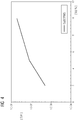
- Figure 4 shows a diagram in which the conductivity of the doped hole transport layer is plotted in Siemens / m as a function of the concentration of the p-dopant in the hole conductor layer.
- substrates on which the conductivity of the doped layers can be measured were coated simultaneously with the samples for the measurement of the current-voltage characteristics.
- differently dimensioned components were produced in order to exclude for the determination of the conductivity that the measured effects depend on the thickness and surface of the components.
- FIG. 4 shows the conductivities as a function of the dopant concentration. The process shown confirms that Figure 3 current-voltage characteristics shown. The conductivity increases the dopant concentration just like the current density.
- the conductivity can only be increased up to material-specific limit values via even higher dopant concentrations, since above a certain concentration it is no longer a matter of doping.
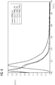
- the Figures 5 , 6th and 7th show the absorption, emission and reflection spectra of the organic hole conductor layers doped with Cu (II) TFMS. For this purpose, these were deposited on quartz glass substrates. These substrates have no electrode contacts and are only used for optical measurements.
- Figure 6 shows the photoluminescence spectra of the hole conductor layers with the Cu (II) TFMS doping in comparison with the spectrum of undoped HTM-014.
- the emission at a wavelength of 432 nm is shifted to 409 nm by the doping.
- a clear shoulder is formed for the doped layers. Shifting and shouldering can be traced back to the formation of a charge transfer complex.
- Figure 7 shows the reflection spectra of the doped hole conductor layers: with increasing dopant concentration, the reflection falls in the blue-green wavelength range and remains in the red range.
- the layers produced therefore have a red cast to the human eye.
- the dependence on the dopant concentration can also be seen optically: the color of the coated substrates becomes darker and redder to the human eye with increasing concentration.
- silver (I) trifluoromethanesulfonate (Ag (I) TFMS) was used.
- the samples shown were also cleaned up: The zone sublimation at a base pressure of 2 ⁇ 10 -4 Pa (2 ⁇ 10 -6 mbar) took place at 370 ° C.-380 ° C. and produced a yield of 47%.
- the purified Ag (I) TFMS was introduced into the hole conductor matrix HTM-014 for doping.
- the substrates, electrodes, layer thicknesses and component size are identical to the Cu (II) TFMS samples.
- Figure 8 shows a current-voltage diagram of an organic semiconductor component with a hole-conducting layer and p-doping with Ag (I) TFMS in different concentrations.
- concentration By varying the concentration, it can be shown that the doping has an effect on the current-voltage characteristic: At 5% doping concentration, an increase in the current density can be seen for negative as well as for small positive voltages ( ⁇ 2V). The characteristics at 5% and 10% concentration are approximately symmetrical and clearly show the successful doping and the improved electrical conductivity. The symmetrical behavior again shows that the hole injection is independent of the work function of the electrodes. At 10% doping concentration, the characteristic curve again reaches the current limit of the measuring device, as already described.
- Figure 9 shows a diagram in which the conductivity of the hole transport layer in Siemens / m is plotted as a function of the concentration of the p-dopant in the hole conductor layer.
- the samples were produced analogously to the Cu (II) TFMS samples.
- the components with the Ag (I) TFMS-doped hole-conducting layers have the following specific conductivities depending on the doping concentration: 2% Ag (I) TFMS in HTM-014: 2.76 x 10⁻⁵ S / m 5% Ag (I) TFMS in HTM-014: 7.66 x 10 -5 S / m 10% Ag (I) TFMS in HTM-014: 7.86 x 10 -5 S / m
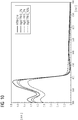
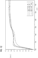
- the Figures 10 , 11 and 12 show the absorption, emission and reflection spectra of the organic hole conductor layers doped with Ag (I) TFMS. For this purpose, these were in turn deposited on quartz glass substrates.
- the absorption spectra in Figure 10 show that the absolute absorption in the absorption maximum at 384 nm wavelength decreases with increasing dopant concentration. At the same time, there is an increase in absorption between 410 nm and 550 nm with increasing dopant concentration. For the visible wavelength range from approx. 400 nm to 700 m, the absorption increases slightly, but in contrast to the Cu (II) TFMS samples, the layers are still color-neutral to the human eye.
- Figure 11 shows the photoluminescence spectra of the hole conductor layers with Ag (I) -TFMS doping. Their comparison with the spectrum of undoped HTM-014 shows that the emission customary from HTM-014 at a wavelength of 432 nm is shifted to 410 nm by the doping. In addition, at 430 nm, a clear shoulder is formed for the doped layers. This shift and shoulder formation is in turn due to the formation of a charge transfer complex.
- Figure 12 shows the reflection spectra of the doped hole conductor layers. With increasing dopant concentration, the reflection in the blue-green wavelength range falls very slightly and remains in the red wavelength range, depending on the dopant concentration. To the human eye, the layers have a neutral color.
Landscapes
- Engineering & Computer Science (AREA)
- Physics & Mathematics (AREA)
- Manufacturing & Machinery (AREA)
- Optics & Photonics (AREA)
- Spectroscopy & Molecular Physics (AREA)
- Chemical & Material Sciences (AREA)
- Materials Engineering (AREA)
- Electroluminescent Light Sources (AREA)
- Photovoltaic Devices (AREA)
Description
- Die vorliegende Erfindung betrifft organische Halbleiterbauelemente und deren Herstellung.
- Im Bereich der organischen Halbleiter ist bekannt, dass zum Transport von Elektronen als Ladungsträger Elektronentransportschichten und zum Transport von Löchern als Ladungsträger Lochtransportschichten eingesetzt werden müssen.
- Eine organische Leuchtdiode ist nur ein Beispiel aus dem Stand der Technik in dem zur Erhöhung der Leitfähigkeit von Ladungstransportschichten und sogenannten "Charge-Generation-Layers" eine Dotierung eingesetzt wird. Auch in organischen Feldeffekttransistoren, Solarzellen oder Fotodetektoren stellt sich das Problem der Dotierung, beispielsweise für Injektionsschichten zur Verringerung des Kontaktwiderstandes, beispielsweise an Source- und Drain-Elektroden oder Elektroden allgemein.
- Grundsätzlich ist für die Dotierung organischer Materialien bekannt, z.B. Dotiermoleküle oder Dotierionen in eine Matrix aus einer organischen Substanz einzubringen. Für die p-Dotierung von Lochleiterschichten werden Elektronenakzeptoren eingebracht. Als derartige zur p-Dotierung geeigneten Elektronenakzeptoren sind beispielsweise Metallkomplexe bekannt. Die bereits bekannten eingesetzten Dotierstoffe haben zumeist Nachteile entweder in der Verarbeitung oder auch in ihrer Auswirkung auf Eigenschaften des Halbleiterbauteils außerhalb des Bereichs der Leitfähigkeitserhöhung. Derartige Bereiche sind z.B. die Effizienz und Lebensdauer. In den meisten organischen Halbleiterbauteilen hängen Effizienz und Lebensdauer stark von der Ladungsträgerdichte an verschiedenen Grenzflächen ab. Insbesondere in organischen Leuchtdioden bestimmt die Exitonendichte in der lichtemittierenden Schicht die Lichtausbeute und Effizienz des Bauteils.
- Was die Verarbeitung der Dotierstoffe zur Herstellung des Bauelements angeht, existiert im Stand der Technik häufig das Problem, dass die Dotierstoffe auf eine Depositionsmethode beschränkt sind und dementsprechend ausschließlich aus der Gasphase oder ausschließlich aus der Flüssigphase verarbeitet werden können. Demnach sind diese Dotierstoffklassen auch auf jeweils eine Materialklasse für die Halbleitermatrix beschränkt. D.h. ein Dotierstoff, der nur aus der Flüssigphase abgeschieden werden kann, kann nur in eine Polymermatrix eingebracht werden. Ein Dotierstoff, der ausschließlich aus der Gasphase abgeschieden werden kann, kann nur in eine "Small-Molecule-Matrix" eingebracht werden. Bei der Eignung für die Abscheidung aus der Gasphase kommt noch hinzu, dass der Dotierstoff auf eine gewisse Temperatur erhitzt werden können muss, ohne dass sich dieser zersetzt. Nur wenn der Dotierstoff geeignet ist in einer Kondensationsreaktion zusammen mit dem Matrixmaterial eine dotierte Lochleiterschicht auszubilden, ist er für den Einsatz in der Bauteilherstellung zu berücksichtigen.
- Neben diesen zusätzlichen Anforderungen an Dotierstoffe wird primär angestrebt, deren Dotierwirkung weiter zu verbessern und dadurch die Leitfähigkeit von organischen Halbleiterschichten weiter zu erhöhen.
- Die
US2010/0109000 A1 offenbart Zusammensetzungen zum Gebrauch in Lochleiterschichten oder Lochinjektionsschichten, Verfahren zur Herstellung dieser Zusammensetzungen, und Vorrichtungen die mit diesen Zusammensetzungen hergestellt werden können. Es können organische Leuchtdioden hergestellt werden. Die Zusammensetzungen bestehen aus zumindest einem leitfähigen konjugierten Polymer, zumindest einer halbleitenden Matrixkomponente, die unterschiedlich von dem leitfähigen konjugierten Polymer ist, und optional einem Dopant, wobei die Zusammensetzungen im Wesentlichen frei von einer isolierenden Matrixkomponente sind. - Es ist Aufgabe der vorliegenden Erfindung, ein Bauelement anzugeben, welches eine Lochleitschicht mit verbesserter Dotierung aufweist. Darüber hinaus ist es Aufgabe der vorliegenden Erfindung, ein Herstellungsverfahren für ein derartiges Bauelement anzugeben.
- Die Aufgabe ist durch eine Vorrichtung gemäß dem Patentanspruch 1 gelöst. Zugehörige Herstellungsverfahren werden in Patentanspruch 4 und Patentanspruch 10 angegeben.
- Vorteilhafte Ausgestaltungen der Erfindung sind Gegenstand der Unteransprüche. Die erfindungsgemäße Vorrichtung ist ein Halbleiterbauelement mit wenigstens einer organischen Lochleiterschicht. Diese Lochleiterschicht weist eine p-Dotierung mit einem Supersäurensalz auf. Das Supersäurensalz weist Silber(I)trifluormethansulfonat (Ag(I)TFMS) und/oder Kupfer(II)trifluormethansulfonat (Cu(II)TFMS) auf.
- Die Substanzklasse der Supersäurensalze erweist sich überraschenderweise als sehr guter p-Dopant in Lochleiterschichten. Vorteil der Erfindung ist eine stark erhöhte Leitfähigkeit der Lochleiterschicht durch Einbringung der Dotierung bei sehr geringen Konzentrationen des Dotierstoffes.
- In einer vorteilhaften Ausgestaltung der Erfindung weist das Halbleiterbauelement eine Lochleiterschicht auf, die eine spezifische Leitfähigkeit von mindestens 2,5 x 10⁻⁵ S/m aufweist, und dabei die Dotierkonzentration bei höchstens 20 Vol.-% liegt. Im Gegensatz zu bisher bekannten Dotierstoffklassen haben die Supersäurensalze den Vorteil bei geringen Konzentrationen in der Lochleitmatrix hohe Leitfähigkeiten zu erwirken.
- In einer weiteren vorteilhaften Ausgestaltung der Erfindung zeigt das Halbleiterbauelement eine Lochleiterschicht auf, die eine p-Dotierung mit einem Supersäurensalz aufweist, wobei das Supersäurensalz Silber(I)trifluormethansulfonat (Ag(I)TFMS) aufweist und das Absorptionsvermögen der Lochleiterschicht im Wellenlängenbereich zwischen 400 nm und 700 nm durch die p-Dotierung mit dem Supersäurensalz im Wesentlichen nicht erhöht wird. Im Wesentlichen nicht erhöht bedeutet, dass der Farbeindruck für das menschliche Auge unverändert bleibt, ob eine Dotierung in die Matrix eingebracht ist oder nicht. Dies hat den Vorteil, dass die Dotierung den Farbeindruck insbesondere im ausgeschalteten Zustand des Bauelements nicht verändert. Der Farbeindruck ist insbesondere bei organischen Leuchtdioden von Bedeutung. Daher ist die erfindungsgemäße Dotierung für den Einsatz in organischen Leuchtdioden besonders bevorzugt.
- Das Silber(I)trifluormethansulfonat hat dabei den Vorteil, die Leitfähigkeit auf bis zu über 7 x 10⁻⁵ S/m zu erhöhen, bei einer Dotierkonzentration von 10 % oder weniger. Dies entspricht einer Erhöhung der Stromdichte bei 1V Bauteilspannung und 200 nm Schichtdicke um 6 Größenordnungen. Der besondere Vorteil von Silber(I)trifluormethansulfonat liegt in der geringen Absorption im sichtbaren Wellenlängenbereich, welche bewirkt, dass die so dotierte Lochleiterschicht für das menschliche Auge farblich neutral erscheint. Das Kupfer(II) trifluormethansulfonat zeichnet sich als p-Dopant besonders dadurch aus, dass es die Leitfähigkeit der Lochleiterschicht auf bis zu über 5 x 10⁻² S/m bei einer Konzentration von 10 % erhöhen kann.
- In einem erfindungsgemäßen Herstellungsverfahren für ein Halbleiterbauelement wird in einem Schritt eine organische Lochleiterschicht, die eine p-Dotierung mit einem Supersäurensalz aufweist, abgeschieden, wobei das Supersäurensalz ein Salz einer Supersäure aufweist, und wobei die Supersäure eine Säure mit einem Säurekonstantewert pKs kleiner als der von Schwefelsäure ist. Hierbei wird für die Abscheidung der Lochleiterschicht ein Matrixmaterial zusammen mit dem Supersäurensalz in einem gemeinsamen Schritt aus der Gasphase abgeschieden, wobei die Dotierkonzentration der Lochleiterschicht über die Verdampfungsraten des Supersäurensalzes und des Matrixmaterials in einer Ko-Verdampfung eingestellt wird.
- Die über die Verdampfungsraten eingestellte Volumenkonzentration des p-Dopanten im Matrixmaterial kann von der tatsächlichen Volumenkonzentration in der fertig abgeschiedenen Lochleiterschicht abweichen.
- Die erfindungsgemäße p-Dotierung mit Supersäurensalzen hat also den Vorteil, über die Wahl von Kation und Säureanion, den Dotierstoff sehr gut an das Matrixmaterial anpassen zu können.
- Besonders die optischen Eigenschaften für den Einsatz des p-Dotierstoffes in organischen Leuchtdioden können durch diese neue Materialklasse für p-Dotierung stark verbessert werden. Eine hohe Leitfähigkeit wird schon bei geringen Dotierkonzentrationen erreicht. Im Bereich der organischen Displays oder Beleuchtungseinrichtungen kann über die erfindungsgemäße p-Dotierung ein Kompromiss zwischen optischen und elektrischen Eigenschaften erwirkt werden. Denn neben dem Dotiereffekt sind auch das optische Erscheinungsbild der dotierten Schichten von Bedeutung für die Qualität eines organischen Halbleiterbauteils, besonders für Displayanwendungen oder Beleuchtungszwecke.
- Nicht einschränkende Beispiele für Supersäuren im Rahmen des oben definierten Begriffs sind:
-
- Fluorsulfonsäure (HSO3F)
- Fluor-Antimonsäure (HSbF6)
- Tetrafluoroborsäure (HBF4)
- Hexafluorophosphorsäure (HPF6)
- Trifluoromethylsulfonsäure (HSO3CF3)
-
- Pentacyanocyclopentadien (HC5(CN)5)
- Teilweise oder ganz fluorierte Derivate des Pentaphenylcyclopentadiens
- Penta-trifluoromethyl-pentadiens bzw. analoger Derviate
- Teilweise oder ganz fluorierte Derivate der Tetraphenylborsäure bzw. deren Cyanoderivate
- Teilweise oder ganz fluorierte Derivate der Arylsulfonsäuren bzw. deren Cyanoderivate
- Teilweise oder ganz fluorierte Derivate der Arylphosphonsäuren bzw. deren Cyanoderivate
- Anionen der Carborane wie beispielsweise [C2B10H10]2- oder [C1B11H10]-
- Die Trifluoromethylsulfonsäure (HSO3CF3) ist davon ein besonders geeigneter Vertreter.
- Die Metallsalze von Supersäuren können mit vielen Kationen erhalten werden, welche beispielsweise aber nicht einschränkend sind:
- Kationen der Alkalimetalle
- Kationen der Erdalkalimetalle
- Kationen der Lanthanoiden (Seltene Erden: La, Ce, Pr, Nd, Sm, Eu, Gd, Tb, Dy, Ho, Er, Tm, Yb, Lu, Y)
- Kationen der Übergangsmetalle
- Aluminium-Kationen
- Kationische Metallkomplexe
- Neben den klassischen Salzen der Alkali- und Erdalkalimetalle sind die Salze der seltenen Erden sowie von Scandium und Aluminium von Bedeutung in der organischen Synthese. Als besonders geeignet haben sich experimentell die Triflate, das heißt die Salze, insbesondere Metallsalze der Supersäure Trifluormethansulfonsäure (TFMS) erwiesen. Diese sehen in allgemeiner Form aus:
(MLn)x+·[O3S-CF3 -]x
Dabei steht M für ein Metall, Ln für einen (n=1) oder mehrere (n=2,3,4,...) Liganden und x für die Ladung des Metallkomplexes. Als Kationen sind also insbesondere alle Kationen komplexer Natur oder Kationen ohne zusätzliche Liganden geeignet. - Die aufgeführten Kationen sind aber auch geeignet mit Anionen anderer Supersäuren Salze zu bilden, die als p-Dotierstoff eingesetzt werden können. Ganz besonders zu bevorzugen sind dabei die Triflate der Übergangsmetalle, insbesondere von Silber und von Kupfer.
- Davon besonders geeignet haben sich:
- Kupfer(II)trifluormethansulfonat (Cu(II)TFMS, CAS-Nr. 34946-82-2, Verdampfungstemperatur: 350°C - 370°C @ 10-5 mbar - 10-6 mbar)

- Silber(I)trifluormethansulfonat (Ag(I)TFMS, CAS-Nr. 2923-28-6, Verdampfungstemperatur: 370°C - 380°C @ 10-5 mbar - 10-6 mbar)

- Überraschenderweise sind viele der so gebildeten Supersäurensalze flüchtig und können insbesondere im Rahmen einer Kokondensationsreaktion zusammen mit einem Lochleiter eine dotierte Lochleiterschicht ausbilden. Die Supersäurensalze sind besonders in wasserfreier Form auch sehr stabil und können sogar weit über 400°C erhitzt werden.
- Kupfer(I)trifluormethansulfonat ist ausschließlich für Lösungsprozessierung geeignet, da es sich nicht unzersetzt verdampfen lässt. Dazu kann Kupfer(I)trifluormethansulfonat beispielsweise im Solvat mit Benzol (C6H6), Toluol (C7H8) oder Acetonitril (C2H3N) verarbeitet werden:
Benzol Toluol Acetonitril 


- Ein wesentlicher Vorteil der Erfindung liegt in der Kostenersparnis. Die Verwendung von Salzen von Supersäuren als p-Doierstoffe für Lochleiterschichten in OLEDs birgt neben dem hohen Dotiervermögen gleichzeitig den Vorteil äußerst geringer Kosten. Die Kosten des derzeit eingesetzter p-Dotierstoffe liegen bei 2000 bis 7000€ /g je nach Abnahmemenge. Ag(I)CF3SO3 und Cu(II) [CF3SO3]2 hingegen liegen bei weniger als 10€/g im normalen Feinchemikalienhandel. Darüber hinaus sind viele Vertreter dieser Klasse kommerziell erhältlich oder zumindest sind deren Herstellverfahren bekannt, gut ausgearbeitet und kostengünstig.
- Organische Lochleiter sind im Allgemeinen aber nicht ausschließlich Abkömmlinge von Triarylaminen.
- Als Lochtransporter, die aus der Gasphase abgeschieden werden können, kommen hierbei insbesondere aber nicht einschränkend in Frage:
- N,N'-Bis(naphthalen-1-yl)-N,N'-bis(phenyl)-9,9-dimethylfluorene
- N,N'-Bis(3-methylphenyl)-N,N'-bis(phenyl)-9,9-diphenylfluorene
- N,N'-Bis(naphthalen-1-yl)-N,N'-bis(phenyl)-9,9-diphenylfluorene
- N,N'-Bis(naphthalen-1-yl)-N,N'-bis(phenyl)-2,2-dimethylbenzidine
- N,N'-Bis(3-methylphenyl)-N,N'-bis(phenyl)-9,9-spirobifluorene
- 2,2',7,7'-Tetrakis(N,N-diphenylamino)-9,9'-spirobifluorene
- N,N'-Bis(naphthalen-1-yl)-N,N'-bis(phenyl)-benzidine
- N,N'-Bis(naphthalen-2-yl)-N,N'-bis(phenyl)-benzidine
- N,N'-Bis(3-methylphenyl)-N,N'-bis(phenyl)-benzidine
- N,N'-Bis(3-methylphenyl)-N,N'-bis(phenyl)-9,9-dimethyl-fluorene
- N,N'-Bis(naphthalen-1-yl)-N,N'-bis(phenyl)-9,9-spirobifluorene
- Di-[4-(N,N-ditolyl-amino)-phenyl]cyclohexane
- 2,2',7,7'-tetra(N, N-di-tolyl)amino-spiro-bifluorene
- 9,9-Bis[4-(N,N-bis-biphenyl-4-yl-amino)phenyl]-9H-fluorene
- 2,2',7,7'-Tetrakis[N-naphthalenyl(phenyl)-amino]-9,9-spirobifluorene
- 2,7-Bis[N,N-bis(9,9-spiro-bifluorene-2-yl)-amino]-9,9-spirobifluorene
- 2,2'-Bis[N,N-bis(biphenyl-4-yl)amino]-9,9-spirobifluorene
- N,N'-bis(phenanthren-9-yl)-N,N'-bis(phenyl)-benzidine
- N,N,N',N'-tetra-naphthalen-2-yl-benzidine
- 2,2'-Bis(N,N-di-phenyl-amino)-9,9-spirobifluorene
- 9,9-Bis[4-(N,N-bis-naphthalen-2-yl-amino)phenyl]-9H-fluorene
- 9,9-Bis[4-(N, N'-bis-naphthalen-2-yl-N,N'-bis-phenyl-amino)-phenyl]-9H-fluorene
- Titanium oxide phthalocyanine
- Copper phthalocyanine
- 2,3,5,6-Tetrafluoro-7,7,8,8,-tetracyano-quinodimethane
- 4,4',4"-Tris(N-3-methylphenyl-N-phenyl-amino)triphenylamine
- 4,4',4"-Tris(N-(2-naphthyl)-N-phenyl-amino)triphenylamine
- 4,4',4"-Tris(N-(1-naphthyl)-N-phenyl-amino)triphenylamine
- 4,4',4"-Tris(N,N-diphenyl-amino)triphenylamine
- Pyrazino[2,3-f][1,10]phenanthroline-2,3-dicarbonitrile
- N, N,N',N'-Tetrakis(4-methoxyphenyl)benzidine
- 2,7-Bis[N,N-bis(4-methoxy-phenyl)amino]-9,9-spirobifluorene
- 2,2'-Bis[N,N-bis(4-methoxy-phenyl)amino]-9,9-spirobifluorene
- N,N'-di(naphthalen-2-yl)-N,N'-diphenylbenzene-1,4-diamine
- N,N'-di-phenyl-N,N'-di-[4-(N,N-di-tolyl-amino)phenyl]benzidine
- N,N'-di-phenyl-N,N'-di-[4-(N, N-di-phenyl-amino)phenyl]benzidine
- NPB (N,N'-Di-[(1-naphthyl)-N,N'-diphenyl]-1,1'-biphenyl)-4,4'-diamine)
- Diese monomolekularen Lochtransportmaterialien können auch aus der Flüssigphase abgeschieden werden oder zu den unten genannten polymeren Materialien in Lösung hinzugemischt werden. Wenn niedermolekulare und polymere Materialien gemischt werden, können über das Mischungsverhältnis (zwischen 0 und 100 %) die Filmbildungseigenschaften beeinflusst und verbessert werden.
- Polymere Lochtransporter, die vornehmlich aus der Flüssigphase abgeschieden werden, sind insbesondere aber nicht einschränkend:
- PEDOT (Poly(3,4 ethylenedioxythiophene)) 
- PVK (poly(9-vinylcarbazole)) 
- PTPD (poly(N,N'-bis(4-butylphenyl)-N,N'-bis(phenyl)-benzidine)) 
- P3HT (poly(3-hexylthiophene)) 
- PANI (polyaniline) 
- Im Sinne der Erfindung sind auch Mischungen aus den genannten polymeren Lochtransportmaterialien.
Als Lösungsmittel kommen bevorzugt organische Lösungsmittel zum Einsatz, wie zum Beispiel: - Benzol,
- Chlorbenzol,
- Chloroform,
- Toluol,
- THF,
- Methoxypropylacetat,
- Anisol,
- Acetonitril,
- Phenetol oder
- Dioxan.
- Ein weiterer besonderer Vorteil der Erfindung besteht darin, dass die für die p-Dotierung geeignete Materialklasse der Supersäurensalze mit der Lochleiter-Matrix aus der gleichen Gasphase abgeschieden wird.
- Dies stellt eine signifikante Vereinfachung der Abscheideverfahren für die Bauteilherstellung dar.
- Neben der besonderen Eignung der Substanzklasse der Supersäurensalze nach Definition der Erfindung für die Abscheidung dotierter Lochleiterschichten aus der Gasphase haben diese den weiteren besonderen Vorteil, dass über die Dotierung das Erscheinungsbild einer OLED im ausgeschalteten Zustand je nach Metallkation und Konzentration einstellbar ist.
- Ausführungsformen der vorliegenden Erfindung werden in exemplarischer Weise mit Bezug auf die
Figuren 1 bis 12 der angehängten Zeichnung beschrieben: - Fig. 1
- Schematischer Aufbau einer organischen Leuchtdiode
- Fig. 2
- Koordination von NPB in die axialen Positionen des Cu(II)-Komplexes
- Fig. 3
- IV-Kennlinien von HTM-014 sowie HTM-014 dotiert mit Cu(II)TFMS
- Fig. 4
- Leitfähigkeiten über der Dotierstoffkonzentration für HTM-014 dotiert mit Cu(II)TFMS
- Fig. 5
- Absorptionsspektra von HTM-014 sowie HTM-014 dotiert mit Cu(II)TFMS
- Fig. 6
- PL-Spektren von HTM-014 und HTM-014 dotiert mit Cu(II)TFMS
- Fig. 7
- Reflexionsspektra von HTM-014 dotiert mit Cu(II)TFMS
- Fig. 8
- IV-Kennlinien von HTM-014 sowie HTM-014 dotiert mit Ag(I)TFMS
- Fig. 9
- Leitfähigkeiten über der Dotierstoffkonzentration für HTM-014 dotiert mit Ag(I)TFMS
- Fig. 10
- Absorptionsspektra von HTM-014 sowie HTM-014 dotiert mit Ag(I)TFMS
- Fig. 11
- PL-Spektren von HTM-014 und HTM-014 dotiert mit Ag(I)TFMS
- Fig. 12
- Reflexionsspektra von HTM-014 dotiert mit Ag(I)TFMS.
- Die
Figur 1 zeigt schematisch den Aufbau eines organischen Halbleiterbauelements 10. Dieser Aufbau wird insbesondere für organische Leuchtdioden verwendet. Dabei werden auf ein Glassubstrat 11 eine untere Elektrode 12 und eine obere Elektrode 13 und dazwischen eine Vielzahl organischer Halbleiterschichten abgeschieden. In derFigur 1 ist ein Querschnitt durch die horizontal angeordneten Schichten gezeigt. An die untere 12 und obere 13 Elektrode kann die Bauteilspannung Ud angelegt werden. In dem gezeigten Fall ist die obere Elektrode 13 die Kathode der Leuchtdiode und die untere Elektrode 12 ist die Anode der Leuchtdiode. Die Lichtauskopplung L geschieht durch das Glassubstrat 11. Dafür ist die Anode transparent, insbesondere aus Indiumzinnoxid (ITO). An die Anode schließen zunächst die Lochleitschichten 20 an. Dabei können diese für unterschiedliche Schwerpunktsfunktionen ausgestaltet sein. Z.B. stellt die erste Schicht 21 auf der Anode eine Lochinjektionsschicht dar. Die daran anschließende Lochleiterschicht 22 eine Lochtransportschicht und die daran weiter anschließende dritte Lochleiterschicht 23 fungiert als elektronblockende Schicht, um die Elektronen, die von der Kathoden-Seite her kommen, daran zu hindern in den Lochleitbereich einzudringen. - Von der Gegenseite, der Kathodenseite her, schließt sich der Elektronentransportbereich an. Dieser kann ebenso mehrere Elektronleitschichten 40 umfassen. Beispielsweise schließt sich an die Kathode eine erste Elektronenleitschicht 43 an, welche als Elektroneninjektionsschicht wirkt. Daran anschließend ist eine zweite Elektronentransportschicht 42 gezeigt und eine dritte Elektronentransportschicht 41 kann wiederum als lochblockende Schicht eingesetzt sein.
- Zwischen dem Elektronentransportbereich und dem Lochtransportbereich befindet sich der Emissionsbereich. Dieser kann wiederum aus mehreren Schichten bestehen. Beispielsweise weist der Emissionsbereich drei Emissionsschichten 30 unterschiedlicher Farbe auf: Eine rote Emissionsschicht 31 schließt an den Lochtransportbereich an, darauf folgt eine grüne Emissionsschicht 32 und eine blaue Emissionsschicht 33 schließt an den Elektrontransportbereich an.
- Für die Stapelung solcher OLED kann die erfindungsgemäße Schicht auch in einer Charge-Generation-Layer verbaut sein. Formal kann die Dotierung durch Koordination von ein bis zwei Lochleitermolekülen, wie z.B. NPB, in die axialen Positionen des Cu(II)-Komplexes vorgenommen werden, wie schematisch in
Figur 2 gezeigt. - Die
Figur 2 zeigt schematisch die verschiedenen Darstellungen der mesomeren Grenzstrukturen des Komplexes: Im Zustand A ist der Dotierstoff, in diesem Beispiel ein Cu(II)-Komplex, nahe an ein Molekül der Lochleitmatrix, in diesem Fall ein NPB-Molekül gebracht. Im Zustand B erfolgt rein formal ein Ladungsübertrag in Form eines Elektrons vom NPB-Molekül auf den Cu(II)-Komplex, d.h. ein Formal-/Partialladungsübertrag einer positiven Ladung auf das NPB-Molekül. Das Kupferatom ist dann nur noch einwertig. Im Zustand C ist gezeigt, dass sich die positive Ladung, auch als Loch bezeichnet, über das NPB-Molekül bewegen kann und im Zustand D auch an ein zweites benachbartes NPB-Molekül übertragen werden kann, was letztendlich dem Hoppingtransport in organischen Halbleitern entspricht. - Diese Koordination kann so stark sein, dass sogar Materialien, die im nicht-koordinierten Zustand bevorzugt elektronenleitend sind, umgepolt werden und zum Lochleiter werden.
- In einem Beispiel kann kommerziell verfügbares Kupfer(II) trifluormethansulfonat (Cu(II)TFMS) mittels Zonensublimation bei einem Basisdruck von 2·10-4 Pa (2·10-6 mbar) aufgereinigt werden. Hierzu kann das Material insbesondere zweimal sublimiert werden, wodurch vorhandene Rückstände und Verunreinigungen entfernt werden. Dazu können Sublimationsschritte bei unterschiedlicher Temperatur vorgenommen werden.
- Für die in den Diagrammen der
Figuren 3 bis 7 gezeigten Proben erfolgte die erste Sublimation des Cu(II)TFMS bei 350°C - 370 °C und erbrachte eine Ausbeute von 79%. Die zweite Sublimation wurde bei 330°C - 345 °C durchgeführt und ergab eine Ausbeute von 89%. Die Gesamtausbeute dieser Aufreinigung betrug damit gut 70%. - Mit diesem Material wurden auf einer ITO-Elektrode (indiumdotiertes Zinnoxid) durch thermisches Verdampfen eine 200 nm dicke dotierte Lochleiterschicht mit dem Lochleiter-Matrixmaterial HTM-014 abgeschieden. Der Lochleiter wird im Folgenden mit HTM-014 bezeichnet. Dieser kann beispielsweise für Bis-N,N,N',N'-(naphthyl-phenyl)benzidin stehen. Als Gegenelektrode wurde eine 150 nm dicke Aluminiumschicht abgeschieden.
-
Figur 3 zeigt ein Stromspannungsdiagramm dieses organischen Halbleiterbauelements aus einer Lochleitschicht mit der Cu(II)TFMS p-Dotierung in unterschiedlichen Konzentrationen von 2%, 5% und 10%. Dabei hat das Bauelement eine Grundfläche von 4 mm2. Eine Referenzmessung der Strom-Spannungs-Kennlinie des undotierten Lochleiters, im Diagramm als "HTM-014" bezeichnet, verdeutlicht den starken Dotiereffekt des Cu(II)TFMS. - Für alle Konzentrationen kann demnach gezeigt werden, dass die Dotierung einen Effekt auf die Strom-Spannungs-Kennlinie hat. Es zeigt sich für alle Konzentrationen ein deutlicher Anstieg der Stromdichten im Vergleich zum undotierten Referenz-Bauteil aus reinem HTM-014.
- Der Dotiereffekt ist insbesondere abhängig von der Dotierstoffkonzentration, was auch durch das Beispiel Cu(II)TFMS in der
Figur 3 gezeigt ist. Die Stromdichte steigt mit steigender Konzentration. Dabei stellen die waagerechten Bereiche der Kennlinien keine Strombegrenzung des Bauteils dar, sondern eine Messgrenze des Messaufbaus. Je kleiner die Spannung Ud, bei der im Bauteil die maximal messbare Stromdichte gemessen wurde, desto besser ist der Dotiereffekt. - Das symmetrische Verhalten der Strom-Spannungs-Kennlinie für positive und negative Betriebsspannungen Ud, zumindest bei Konzentrationen von 5% und 10% zeigt, dass die Lochinjektion unabhängig ist von der Austrittsarbeit der Elektroden und daher für die Aluminium- sowie die ITO-Elektrode gleich gut funktioniert. Die 2%-Probe zeigt kein vollständig symmetrisches Verhalten, da das Matrixmaterial ein Lochtransporter ist. Die Dotierkonzentration von 2% ist noch nicht ausreichend um eine zur ITO-Elektrode vergleichbare Injektion aus der Aluminium-Elektrode zu erreichen.
-
Figur 4 zeigt ein Diagramm, in dem die Leitfähigkeit der dotierten Lochtransportschicht in Siemens/m in Abhängigkeit von der Konzentration des p-Dopanten in der Lochleiterschicht aufgetragen ist. Dazu wurden gleichzeitig mit den Proben für die Messung der Strom-Spannungs-Kennlinien Substrate beschichtet, auf denen die Leitfähigkeit der dotierten Schichten gemessen werden kann. Dazu wurden verschieden dimensionierte Bauteile erzeugt um für die Bestimmung der Leitfähigkeit auszuschließen, dass die gemessenen Effekte von Dicke und Fläche der Bauelemente abhängen. Daraus ergeben sich für die gewählten Dotierkonzentrationen folgende spezifische Werte:2% Cu(II)TFMS in HTM-014: 1,99·10-3 S/m 5% Cu(II)TFMS in HTM-014: 1,24·10-2 S/m 10% Cu(II)TFMS in HTM-014: 5,25·10-2 S/m - Das Diagramm in
Figur 4 zeigt die Leitfähigkeiten in Abhängigkeit von der Dotierstoffkonzentration. Der gezeigte Verlauf bestätigt dieFigur 3 gezeigten Strom-Spannungs-Kennlinien. Die Leitfähigkeit steigt der Dotierstoffkonzentration genau wie die Stromdichte. - Die Leitfähigkeit ist über noch höhere Dotierstoffkonzentrationen nur bis zu materialspezifischen Grenzwerten steigerbar, da es sich ab einer gewissen Konzentration nicht mehr um einen Dotierung handelt.
- Die
Figuren 5 ,6 und7 zeigen die Absorptions-, Emissions- und Reflexionsspektren der mit Cu(II)TFMS dotierten organischen Lochleiterschichten. Dazu wurden diese auf Quarzglassubstraten abgeschieden. Diese Substrate besitzen keine Elektroden-Kontakte und dienen nur zur optischen Messung. - Die Absorptionsspektren in
Figur 5 zeigen, dass die absolute Absorption im Absorptionsmaximum bei 384 nm Wellenlänge mit steigender Dotierstoffkonzentration abfällt. Die Absorption des HTM-014 unterhalb von 400 nm wird also durch die Dotierung gesenkt, was an der Bildung eines Charge-Transfer Komplexes liegt. - Gleichzeitig kommt es zu einem Anstieg der Absorption zwischen 410 nm und 550 nm. Auch in diesem Bereich steigt die Absorption mit steigender Dotierstoffkonzentration. Für den sichtbaren Wellenlängenbereich von circa 400nm bis 700 nm steigt also die Absorption im blauen bis grünen Wellenlängenbereich wodurch die Schichten für das menschliche Auge rötlich erscheinen.
-
Figur 6 zeigt die Fotolumineszenzspektren der Lochleiterschichten mit der Cu(II)TFMS-Dotierung im Vergleich mit dem Spektrum von undotiertem HTM-014. Die Emission bei einer Wellenlänge von 432 nm wird durch die Dotierung auf 409 nm verschoben. Außerdem bildet sich bei 430 nm eine deutliche Schulter für die dotierten Schichten aus. Verschiebung und Schulterbildung können auf die Bildung eines Charge-Transfer Komplexes zurück geführt werden. -
Figur 7 zeigt die Reflexionsspektren der dotierten Lochleiterschichten: Mit steigender Dotierstoffkonzentration fällt die Reflexion im blau-grünen Wellenlängenbereich und bleibt im roten Bereich erhalten. Daher besitzen die erzeugten Schichten einen für das menschliche Auge roten Stich. Auch optisch ist die Abhängigkeit von der Dotierstoffkonzentration zu sehen: Der Farbton der beschichteten Substrate wird für das menschliche Auge mit steigender Konzentration immer dunkler und roter. - In einem weiteren Beispiel wurde kommerziell verfügbares Silber(I) trifluormethansulfonat (Ag(I)TFMS) verwendet. Für die in den Diagrammen der
Figuren 8 bis 12 gezeigten Proben erfolgte auch eine Aufreinigung des Materials: Die Zonensublimation bei einem Basisdruck von 2·10-4 Pa (2·10-6 mbar) erfolgte bei 370°C - 380°C und erbrachte eine Ausbeute von 47%. Analog Beispiel Cu(II)TFMS wurde das aufgereinigte Ag(I)TFMS zur Dotierung in die Lochleiter-Matrix HTM-014 eingebracht. Substrate, Elektroden, Schichtdicken und Bauteilgröße sind hierbei identisch zu den Cu(II)TFMS-Proben. -
Figur 8 zeigt ein Stromspannungsdiagramm eines organischen Halbleiterbauelements mit einer Lochleitschicht und einer p-Dotierung mit Ag(I)TFMS in unterschiedlichen Konzentrationen. Durch die Variation der Konzentration kann gezeigt werden, dass die Dotierung einen Effekt auf die Strom-Spannungs-Kennlinie hat: Bei 5% Dotier-Konzentration ist eine Erhöhung der Stromdichte für negative sowie für kleine positive Spannungen (<2V) zu sehen. Die Kennlinie bei 5% und 10% Konzentration sind annähernd symmetrisch und zeigen deutlich die erfolgreiche Dotierung und die verbesserte Stromleitfähigkeit. Das symmetrische Verhalten zeigt wiederum, dass die Lochinjektion unabhängig ist von der Austrittsarbeit der Elektroden. Bei 10% Dotier-Konzentration erreicht die Kennlinie wieder die Strombegrenzung des Messgerätes, wie bereits beschrieben. -
Figur 9 zeigt ein Diagramm, in dem die Leitfähigkeit der Lochtransportschicht in Siemens/m in Abhängigkeit von der Konzentration des p-Dopanten in der Lochleiterschicht aufgetragen ist. Die Proben wurden analog zu den Cu(II)TFMS-Proben hergestellt. Die Bauelemente mit den Ag(I)TFMS-dotierten Lochleitschichten weisen folgende spezifische Leitfähigkeiten in Abhängigkeit von der Dotierkonzentration auf:2% Ag(I)TFMS in HTM-014: 2,76·10~5 S/m 5% Ag(I)TFMS in HTM-014: 7,66·10-5 S/m 10% Ag(I)TFMS in HTM-014: 7,86·10-5 S/m - Die
Figuren 10 ,11 und12 zeigen die Absorptions-, Emissions- und Reflexionsspektren der mit Ag(I)TFMS dotierten organischen Lochleiterschichten. Dazu wurden diese wiederum auf Quarzglassubstraten abgeschieden. - Die Absorptionsspektren in
Figur 10 zeigen, dass die absolute Absorption im Absorptionsmaximum bei 384 nm Wellenlänge mit steigender Dotierstoffkonzentration abfällt. Gleichzeitig kommt es zu einem Anstieg der Absorption zwischen 410 nm und 550 nm mit steigender Dotierstoffkonzentration. Für den sichtbaren Wellenlängenbereich von circa 400 nm bis 700 m steigt die Absorption zwar leicht an, aber im Gegensatz zu den Cu(II)TFMS-Proben sind die Schichten für das menschliche Auge farblich weiterhin neutral. -
Figur 11 zeigt die Fotolumineszenzspektren der Lochleiterschichten mit Ag(I)-TFMS-Dotierung. Deren Vergleich dem Spektrum von undotiertem HTM-014 zeigt, dass sich die vom HTM-014 übliche Emission bei einer Wellenlänge von 432 nm durch die Dotierung auf 410 nm verschiebt. Außerdem bildet sich bei 430 nm eine deutliche Schulter für die dotierten Schichten aus. Diese Verschiebung und Schulterbildung ist wiederum auf die Bildung eines Charge-Transfer Komplexes zurück zu führen. -
Figur 12 zeigt die Reflexionsspektren der dotierten Lochleiterschichten. Mit steigender Dotierstoffkonzentration fällt die Reflexion im blau-grünen Wellenlängenbereich sehr leicht ab und bleibt im roten Wellenlängenbereich erhalten, abhängig von der Dotierstoffkonzentration. Für das menschliche Auge weisen die Schichten einen neutralen Farbton auf.
Claims (10)
- Halbleiterbauelement (10) mit wenigstens einer organischen Lochleiterschicht (20), die eine p-Dotierung mit einem Supersäurensalz aufweist, dadurch gekennzeichnet, dass das Supersäurensalz Silber(I)trifluormethansulfonat (Ag(I)TFMS) und/oder Kupfer(II)trifluormethansulfonat (Cu(II)TFMS) aufweist.
- Halbleiterbauelement (10) nach Anspruch 1, wobei die Lochleiterschicht (20), die eine p-Dotierung mit einem Supersäurensalz aufweist, eine spezifische Leitfähigkeit von mindestens 2,5·10-5 S/m bei einer Dotierkonzentration von höchstens 20 Vol.-% aufweist.
- Halbleiterbauelement (10) nach einem der vorstehenden Ansprüche, wobei das Supersäurensalz Silber(I)trifluormethansulfonat (Ag(I)TFMS) aufweist und das Absorptionsvermögen der Lochleiterschicht (20) im Wellenlängenbereich zwischen 400 nm und 700 nm durch die p-Dotierung mit dem Supersäuresalz im Wesentlichen nicht erhöht wird, so dass der Farbeindruck für das menschliche Auge unverändert bleibt.
- Herstellungsverfahren für ein Halbleiterbauelement (10) mit einem Schritt zur Abscheidung einer organischen Lochleiterschicht (20), die eine p-Dotierung mit einem Supersäurensalz aufweist, dadurch gekennzeichnet, dass das Supersäurensalz Silber(I)trifluormethansulfonat (Ag(I)TFMS) und/oder Kupfer(II)trifluormethansulfonat (Cu(II)TFMS) aufweist.
- Herstellungsverfahren nach Anspruch 4, wobei für die Abscheidung der Lochleiterschicht (20) ein Matrixmaterial zusammen mit dem Supersäurensalz in einem gemeinsamen Schritt abgeschieden wird.
- Herstellungsverfahren nach einem der Ansprüche 4 oder 5, wobei Matrixmaterial und das Supersäurensalz aus der Gasphase, insbesondere durch thermisches Verdampfen abgeschieden werden.
- Herstellungsverfahren nach Anspruch 5 und Anspruch 6, wobei die Dotierkonzentration der Lochleiterschicht (20) über die Verdampfungsraten des Supersäurensalzes und des Matrixmaterials in einer Ko-Verdampfung eingestellt wird.
- Herstellungsverfahren nach einem der Ansprüche 4 oder 5, wobei Matrixmaterial und das Supersäurensalz aus Lösung abgeschieden werden.
- Herstellungsverfahren nach Anspruch 5 und Anspruch 8, wobei die Dotierkonzentration der Lochleiterschicht (20) über den Massenanteil des Supersäurensalzes und des Matrixmaterials in der Lösung vor der Abscheidung eingestellt wird.
- Herstellungsverfahren für ein Halbleiterbauelement (10) mit einem Schritt zur Abscheidung einer organischen Lochleiterschicht (20), die eine p-Dotierung mit einem Supersäurensalz aufweist, wobei das Supersäurensalz ein Salz einer Supersäure aufweist, und wobei die Supersäure eine Säure mit einem Säurekonstantewert pKs kleiner als der von Schwefelsäure ist, dadurch gekennzeichnet, dass für die Abscheidung der Lochleiterschicht (20) ein Matrixmaterial zusammen mit dem Supersäurensalz in einem gemeinsamen Schritt aus der Gasphase abgeschieden wird, wobei die Dotierkonzentration der Lochleiterschicht (20) über die Verdampfungsraten des Supersäurensalzes und des Matrixmaterials in einer Ko-Verdampfung eingestellt wird.
Applications Claiming Priority (2)
| Application Number | Priority Date | Filing Date | Title |
|---|---|---|---|
| DE102011003192.8A DE102011003192B4 (de) | 2011-01-26 | 2011-01-26 | Halbleiterbauelement und Verfahren zu seiner Herstellung |
| PCT/EP2012/050117 WO2012100972A1 (de) | 2011-01-26 | 2012-01-05 | Organisches halbleiterbauelement mit dotierter lochleiterschicht |
Publications (2)
| Publication Number | Publication Date |
|---|---|
| EP2656412A1 EP2656412A1 (de) | 2013-10-30 |
| EP2656412B1 true EP2656412B1 (de) | 2020-11-18 |
Family
ID=45446061
Family Applications (1)
| Application Number | Title | Priority Date | Filing Date |
|---|---|---|---|
| EP12700039.6A Active EP2656412B1 (de) | 2011-01-26 | 2012-01-05 | Organisches halbleiterbauelement mit dotierter lochleiterschicht |
Country Status (7)
| Country | Link |
|---|---|
| US (1) | US9263696B2 (de) |
| EP (1) | EP2656412B1 (de) |
| JP (1) | JP5869590B2 (de) |
| KR (1) | KR101991525B1 (de) |
| CN (1) | CN103339753B (de) |
| DE (1) | DE102011003192B4 (de) |
| WO (1) | WO2012100972A1 (de) |
Families Citing this family (10)
| Publication number | Priority date | Publication date | Assignee | Title |
|---|---|---|---|---|
| DE102011003192B4 (de) | 2011-01-26 | 2015-12-24 | Siemens Aktiengesellschaft | Halbleiterbauelement und Verfahren zu seiner Herstellung |
| DE102013106949A1 (de) | 2013-07-02 | 2015-01-08 | Osram Opto Semiconductors Gmbh | Optoelektronisches Bauelement, organische funktionelle Schicht und Verfahren zur Herstellung eines optoelektronischen Bauelements |
| DE102013107415A1 (de) * | 2013-07-12 | 2015-01-15 | Osram Opto Semiconductors Gmbh | Organisches lichtemittierendes Bauelement und Verfahren zur Herstellung eines organischen lichtemittierenden Bauelements |
| DE102014210412A1 (de) * | 2014-06-03 | 2015-12-03 | Siemens Aktiengesellschaft | p-Dotierende Vernetzung organischer Lochleiter |
| GB2527606A (en) * | 2014-06-27 | 2015-12-30 | Cambridge Display Tech Ltd | Charge-transfer salt |
| DE102015121844A1 (de) | 2015-12-15 | 2017-06-22 | Osram Oled Gmbh | Organisches elektronisches Bauelement und Verwendung eines fluorierten Sulfonimid-Metallsalzes |
| DE102017111425A1 (de) | 2017-05-24 | 2018-11-29 | Osram Oled Gmbh | Organisches elektronisches Bauelement und Verfahren zur Herstellung eines organischen elektronischen Bauelements |
| DE102018212305A1 (de) | 2018-07-24 | 2020-01-30 | Siemens Aktiengesellschaft | Metallorganische Perowskit-Solarzelle, Tandem-Solarzelle sowie Herstellungsverfahren dazu |
| DE102018212304A1 (de) | 2018-07-24 | 2020-01-30 | Siemens Aktiengesellschaft | Metallorganische Perowskit-Solarzelle, Tandem-Solarzelle sowie Herstellungsverfahren dazu |
| EP3859811B1 (de) * | 2020-01-28 | 2025-03-19 | Novaled GmbH | Organische elektronische vorrichtung mit einer anodenschicht, einer kathodenschicht, mindestens einer emissionsschicht (eml) und mindestens einer lochinjektionsschicht (hil) |
Citations (1)
| Publication number | Priority date | Publication date | Assignee | Title |
|---|---|---|---|---|
| WO2006086480A2 (en) * | 2005-02-10 | 2006-08-17 | Plextronics, Inc. | Hole injection/transport layer compositions and devices |
Family Cites Families (21)
| Publication number | Priority date | Publication date | Assignee | Title |
|---|---|---|---|---|
| US5853906A (en) * | 1997-10-14 | 1998-12-29 | Xerox Corporation | Conductive polymer compositions and processes thereof |
| JPH11251067A (ja) | 1998-03-02 | 1999-09-17 | Junji Kido | 有機エレクトロルミネッセント素子 |
| JP4363050B2 (ja) | 2002-01-31 | 2009-11-11 | 住友化学株式会社 | 有機エレクトロルミネッセンス素子 |
| WO2003065770A1 (fr) * | 2002-01-31 | 2003-08-07 | Sumitomo Chemical Company, Limited | Dispositif d'electroluminescence organique |
| JP2003272865A (ja) | 2002-03-19 | 2003-09-26 | Mitsubishi Rayon Co Ltd | 有機電界発光素子 |
| US7390438B2 (en) * | 2003-04-22 | 2008-06-24 | E.I. Du Pont De Nemours And Company | Water dispersible substituted polydioxythiophenes made with fluorinated polymeric sulfonic acid colloids |
| GB0311234D0 (en) | 2003-05-16 | 2003-06-18 | Isis Innovation | Organic phosphorescent material and organic optoelectronic device |
| US7455793B2 (en) | 2004-03-31 | 2008-11-25 | E.I. Du Pont De Nemours And Company | Non-aqueous dispersions comprising electrically doped conductive polymers and colloid-forming polymeric acids |
| US20060008671A1 (en) * | 2004-07-07 | 2006-01-12 | Raymond Kwong | Electroluminescent efficiency |
| US7851072B2 (en) | 2005-05-19 | 2010-12-14 | Universal Display Corporation | Stable and efficient electroluminescent materials |
| EP1899985A4 (de) | 2005-06-27 | 2010-03-10 | Du Pont | Elektrisch leitfähige polymerzusammensetzungen |
| WO2008057615A2 (en) * | 2006-03-03 | 2008-05-15 | Eikos, Inc. | Highly transparent and conductive carbon nanotube coatings |
| DE102007028238A1 (de) | 2007-06-20 | 2008-12-24 | Osram Opto Semiconductors Gmbh | Verwendung eines Metallkomplexes als p-Dotand für ein organisches halbleitendes Matrixmaterial, organisches Halbleitermaterial und organische Leuchtdiode |
| KR101435999B1 (ko) * | 2007-12-07 | 2014-08-29 | 삼성전자주식회사 | 도펀트로 도핑된 산화그라펜의 환원물, 이를 포함하는 박막및 투명전극 |
| KR20090092114A (ko) * | 2008-02-26 | 2009-08-31 | 삼성모바일디스플레이주식회사 | 초강산의 염을 포함하는 전자 주입층, 이를 포함하는광전변환 소자 및 이를 포함하는 유기 발광 소자 |
| JP5104428B2 (ja) | 2008-03-13 | 2012-12-19 | コニカミノルタホールディングス株式会社 | 有機半導体材料、これを用いた電界効果トランジスタ |
| KR101762964B1 (ko) | 2008-10-27 | 2017-07-28 | 닛산 가가쿠 고교 가부시키 가이샤 | 전하 주입 및 수송 층 |
| JP2010265236A (ja) | 2009-05-18 | 2010-11-25 | Sumitomo Chemical Co Ltd | 含シリルチアゾリウムヨーダイド又は含シリルオキサゾリウムヨーダイド及びその用途 |
| US8580394B2 (en) * | 2009-11-19 | 2013-11-12 | Universal Display Corporation | 3-coordinate copper(I)-carbene complexes |
| DE102010056519B4 (de) * | 2010-12-27 | 2024-11-28 | Heliatek Gmbh | Optoelektronisches Bauelement mit dotierten Schichten |
| DE102011003192B4 (de) | 2011-01-26 | 2015-12-24 | Siemens Aktiengesellschaft | Halbleiterbauelement und Verfahren zu seiner Herstellung |
-
2011
- 2011-01-26 DE DE102011003192.8A patent/DE102011003192B4/de active Active
-
2012
- 2012-01-05 JP JP2013550813A patent/JP5869590B2/ja active Active
- 2012-01-05 US US13/982,053 patent/US9263696B2/en active Active
- 2012-01-05 KR KR1020137022295A patent/KR101991525B1/ko active Active
- 2012-01-05 CN CN201280006603.1A patent/CN103339753B/zh active Active
- 2012-01-05 WO PCT/EP2012/050117 patent/WO2012100972A1/de not_active Ceased
- 2012-01-05 EP EP12700039.6A patent/EP2656412B1/de active Active
Patent Citations (1)
| Publication number | Priority date | Publication date | Assignee | Title |
|---|---|---|---|---|
| WO2006086480A2 (en) * | 2005-02-10 | 2006-08-17 | Plextronics, Inc. | Hole injection/transport layer compositions and devices |
Non-Patent Citations (1)
| Title |
|---|
| AGNES KÜTT ET AL: "Equilibrium Acidities of Superacids", JOURNAL OF ORGANIC CHEMISTRY, vol. 76, no. 2, 17 December 2010 (2010-12-17), US, pages 391 - 395, XP055235130, ISSN: 0022-3263, DOI: 10.1021/jo101409p * |
Also Published As
| Publication number | Publication date |
|---|---|
| DE102011003192A1 (de) | 2012-07-26 |
| KR101991525B1 (ko) | 2019-06-20 |
| JP5869590B2 (ja) | 2016-02-24 |
| US9263696B2 (en) | 2016-02-16 |
| EP2656412A1 (de) | 2013-10-30 |
| WO2012100972A1 (de) | 2012-08-02 |
| JP2014511021A (ja) | 2014-05-01 |
| CN103339753B (zh) | 2016-11-09 |
| DE102011003192B4 (de) | 2015-12-24 |
| KR20140007395A (ko) | 2014-01-17 |
| CN103339753A (zh) | 2013-10-02 |
| US20140034934A1 (en) | 2014-02-06 |
Similar Documents
| Publication | Publication Date | Title |
|---|---|---|
| EP2656412B1 (de) | Organisches halbleiterbauelement mit dotierter lochleiterschicht | |
| EP2553047B1 (de) | Dotierstoff für eine lochleiterschicht für organische halbleiterbauelemente und verwendung dazu | |
| DE102012101652B4 (de) | Organisches halbleitendes Material und elektronisches Bauelement | |
| EP3246960B1 (de) | Hauptgruppenmetallkomplexe als p-dotanden für organische elektronische matrixmaterialien | |
| EP1656706B1 (de) | Organisches elektrolumineszenzelement | |
| DE60306570T2 (de) | Organische elektrolumineszente Vorrichtungen | |
| DE102008051737B4 (de) | Quadratisch planare Übergangsmetallkomplexe, organische halbleitende Materialien sowie elektronische oder optoelektronische Bauelemente, die diese umfassen und Verwendung derselben | |
| DE102007018456B4 (de) | Verwendung von Hauptgruppenelementhalogeniden und/oder -pseudohalogeniden, organisches halbleitendes Matrixmaterial, elektronische und optoelektronische Bauelemente | |
| DE112008004292B3 (de) | Licht emittierendes Bauelement und Verfahren zum Herstellen | |
| EP2483945B1 (de) | Organische elektronische vorrichtung und verfahren zu deren herstellung | |
| EP2691997B1 (de) | Komplexierung niedermolekularer halbleiter für die anwendung als emitterkomplex in organischen lichtemittierenden elektrochemischen zellen (oleecs) | |
| EP2158625B1 (de) | Verwendung eines metallkomplexes als p-dotand für ein organisches halbleitendes matrixmaterial, organisches halbleitermaterial und organische leuchtdioden | |
| WO2005036667A1 (de) | N- dotierung von organischen halbleitern | |
| EP1786050A1 (de) | Dotiertes organisches Halbleitermaterial | |
| EP1668718B1 (de) | Organisches elektrolumineszenzelement | |
| WO2008058525A2 (de) | Verwendung einer koordinationsverbindung zur dotierung von organischen halbleitern | |
| EP1806795B1 (de) | Organisches Bauelement | |
| EP2768926A1 (de) | Organisches elektronisches bauelement mit dotierstoff, verwendung eines dotierstoffs und verfahren zur herstellung des dotierstoffs | |
| EP3201959B1 (de) | Organisches elektronisches bauteil | |
| EP2483943B1 (de) | Optoelektronisches organisches bauelement und verfahren zu dessen herstellung | |
| EP1643568A1 (de) | Verfahren zum Herstellen einer Schicht aus einem dotierten Halbleitermaterial und Vorrichtung | |
| WO2010057471A1 (de) | Chinoxalinverbindungen und halbleitermaterialien | |
| WO2017178473A1 (de) | Organisches elektronisches bauteil mit ladungsträger-generationsschicht | |
| DE102018212304A1 (de) | Metallorganische Perowskit-Solarzelle, Tandem-Solarzelle sowie Herstellungsverfahren dazu | |
| DE102007059887B4 (de) | Lichtemittierendes organisches Bauelement und Verfahren zu dessen Herstellung |
Legal Events
| Date | Code | Title | Description |
|---|---|---|---|
| PUAI | Public reference made under article 153(3) epc to a published international application that has entered the european phase |
Free format text: ORIGINAL CODE: 0009012 |
|
| 17P | Request for examination filed |
Effective date: 20130614 |
|
| AK | Designated contracting states |
Kind code of ref document: A1 Designated state(s): AL AT BE BG CH CY CZ DE DK EE ES FI FR GB GR HR HU IE IS IT LI LT LU LV MC MK MT NL NO PL PT RO RS SE SI SK SM TR |
|
| RIN1 | Information on inventor provided before grant (corrected) |
Inventor name: KELLERMANN, RENATE Inventor name: SCHMID, GUENTER Inventor name: MALTENBERGER, ANNA Inventor name: WEMKEN, JAN HAUKE |
|
| DAX | Request for extension of the european patent (deleted) | ||
| RAP1 | Party data changed (applicant data changed or rights of an application transferred) |
Owner name: SIEMENS AKTIENGESELLSCHAFT |
|
| STAA | Information on the status of an ep patent application or granted ep patent |
Free format text: STATUS: EXAMINATION IS IN PROGRESS |
|
| 17Q | First examination report despatched |
Effective date: 20190719 |
|
| GRAP | Despatch of communication of intention to grant a patent |
Free format text: ORIGINAL CODE: EPIDOSNIGR1 |
|
| STAA | Information on the status of an ep patent application or granted ep patent |
Free format text: STATUS: GRANT OF PATENT IS INTENDED |
|
| INTG | Intention to grant announced |
Effective date: 20200316 |
|
| GRAS | Grant fee paid |
Free format text: ORIGINAL CODE: EPIDOSNIGR3 |
|
| GRAA | (expected) grant |
Free format text: ORIGINAL CODE: 0009210 |
|
| STAA | Information on the status of an ep patent application or granted ep patent |
Free format text: STATUS: THE PATENT HAS BEEN GRANTED |
|
| AK | Designated contracting states |
Kind code of ref document: B1 Designated state(s): AL AT BE BG CH CY CZ DE DK EE ES FI FR GB GR HR HU IE IS IT LI LT LU LV MC MK MT NL NO PL PT RO RS SE SI SK SM TR |
|
| RAP1 | Party data changed (applicant data changed or rights of an application transferred) |
Owner name: NOVALED GMBH |
|
| REG | Reference to a national code |
Ref country code: GB Ref legal event code: FG4D Free format text: NOT ENGLISH |
|
| REG | Reference to a national code |
Ref country code: CH Ref legal event code: EP |
|
| REG | Reference to a national code |
Ref country code: IE Ref legal event code: FG4D Free format text: LANGUAGE OF EP DOCUMENT: GERMAN |
|
| REG | Reference to a national code |
Ref country code: DE Ref legal event code: R096 Ref document number: 502012016482 Country of ref document: DE |
|
| REG | Reference to a national code |
Ref country code: AT Ref legal event code: REF Ref document number: 1336739 Country of ref document: AT Kind code of ref document: T Effective date: 20201215 |
|
| REG | Reference to a national code |
Ref country code: NL Ref legal event code: MP Effective date: 20201118 |
|
| PG25 | Lapsed in a contracting state [announced via postgrant information from national office to epo] |
Ref country code: RS Free format text: LAPSE BECAUSE OF FAILURE TO SUBMIT A TRANSLATION OF THE DESCRIPTION OR TO PAY THE FEE WITHIN THE PRESCRIBED TIME-LIMIT Effective date: 20201118 Ref country code: FI Free format text: LAPSE BECAUSE OF FAILURE TO SUBMIT A TRANSLATION OF THE DESCRIPTION OR TO PAY THE FEE WITHIN THE PRESCRIBED TIME-LIMIT Effective date: 20201118 Ref country code: NO Free format text: LAPSE BECAUSE OF FAILURE TO SUBMIT A TRANSLATION OF THE DESCRIPTION OR TO PAY THE FEE WITHIN THE PRESCRIBED TIME-LIMIT Effective date: 20210218 Ref country code: PT Free format text: LAPSE BECAUSE OF FAILURE TO SUBMIT A TRANSLATION OF THE DESCRIPTION OR TO PAY THE FEE WITHIN THE PRESCRIBED TIME-LIMIT Effective date: 20210318 Ref country code: GR Free format text: LAPSE BECAUSE OF FAILURE TO SUBMIT A TRANSLATION OF THE DESCRIPTION OR TO PAY THE FEE WITHIN THE PRESCRIBED TIME-LIMIT Effective date: 20210219 |
|
| PG25 | Lapsed in a contracting state [announced via postgrant information from national office to epo] |
Ref country code: SE Free format text: LAPSE BECAUSE OF FAILURE TO SUBMIT A TRANSLATION OF THE DESCRIPTION OR TO PAY THE FEE WITHIN THE PRESCRIBED TIME-LIMIT Effective date: 20201118 Ref country code: PL Free format text: LAPSE BECAUSE OF FAILURE TO SUBMIT A TRANSLATION OF THE DESCRIPTION OR TO PAY THE FEE WITHIN THE PRESCRIBED TIME-LIMIT Effective date: 20201118 Ref country code: IS Free format text: LAPSE BECAUSE OF FAILURE TO SUBMIT A TRANSLATION OF THE DESCRIPTION OR TO PAY THE FEE WITHIN THE PRESCRIBED TIME-LIMIT Effective date: 20210318 Ref country code: LV Free format text: LAPSE BECAUSE OF FAILURE TO SUBMIT A TRANSLATION OF THE DESCRIPTION OR TO PAY THE FEE WITHIN THE PRESCRIBED TIME-LIMIT Effective date: 20201118 Ref country code: BG Free format text: LAPSE BECAUSE OF FAILURE TO SUBMIT A TRANSLATION OF THE DESCRIPTION OR TO PAY THE FEE WITHIN THE PRESCRIBED TIME-LIMIT Effective date: 20210218 |
|
| REG | Reference to a national code |
Ref country code: LT Ref legal event code: MG9D |
|
| PG25 | Lapsed in a contracting state [announced via postgrant information from national office to epo] |
Ref country code: HR Free format text: LAPSE BECAUSE OF FAILURE TO SUBMIT A TRANSLATION OF THE DESCRIPTION OR TO PAY THE FEE WITHIN THE PRESCRIBED TIME-LIMIT Effective date: 20201118 |
|
| PG25 | Lapsed in a contracting state [announced via postgrant information from national office to epo] |
Ref country code: SK Free format text: LAPSE BECAUSE OF FAILURE TO SUBMIT A TRANSLATION OF THE DESCRIPTION OR TO PAY THE FEE WITHIN THE PRESCRIBED TIME-LIMIT Effective date: 20201118 Ref country code: RO Free format text: LAPSE BECAUSE OF FAILURE TO SUBMIT A TRANSLATION OF THE DESCRIPTION OR TO PAY THE FEE WITHIN THE PRESCRIBED TIME-LIMIT Effective date: 20201118 Ref country code: LT Free format text: LAPSE BECAUSE OF FAILURE TO SUBMIT A TRANSLATION OF THE DESCRIPTION OR TO PAY THE FEE WITHIN THE PRESCRIBED TIME-LIMIT Effective date: 20201118 Ref country code: SM Free format text: LAPSE BECAUSE OF FAILURE TO SUBMIT A TRANSLATION OF THE DESCRIPTION OR TO PAY THE FEE WITHIN THE PRESCRIBED TIME-LIMIT Effective date: 20201118 Ref country code: EE Free format text: LAPSE BECAUSE OF FAILURE TO SUBMIT A TRANSLATION OF THE DESCRIPTION OR TO PAY THE FEE WITHIN THE PRESCRIBED TIME-LIMIT Effective date: 20201118 Ref country code: CZ Free format text: LAPSE BECAUSE OF FAILURE TO SUBMIT A TRANSLATION OF THE DESCRIPTION OR TO PAY THE FEE WITHIN THE PRESCRIBED TIME-LIMIT Effective date: 20201118 |
|
| REG | Reference to a national code |
Ref country code: DE Ref legal event code: R097 Ref document number: 502012016482 Country of ref document: DE |
|
| PG25 | Lapsed in a contracting state [announced via postgrant information from national office to epo] |
Ref country code: DK Free format text: LAPSE BECAUSE OF FAILURE TO SUBMIT A TRANSLATION OF THE DESCRIPTION OR TO PAY THE FEE WITHIN THE PRESCRIBED TIME-LIMIT Effective date: 20201118 Ref country code: MC Free format text: LAPSE BECAUSE OF FAILURE TO SUBMIT A TRANSLATION OF THE DESCRIPTION OR TO PAY THE FEE WITHIN THE PRESCRIBED TIME-LIMIT Effective date: 20201118 |
|
| REG | Reference to a national code |
Ref country code: CH Ref legal event code: PL |
|
| PLBE | No opposition filed within time limit |
Free format text: ORIGINAL CODE: 0009261 |
|
| STAA | Information on the status of an ep patent application or granted ep patent |
Free format text: STATUS: NO OPPOSITION FILED WITHIN TIME LIMIT |
|
| PG25 | Lapsed in a contracting state [announced via postgrant information from national office to epo] |
Ref country code: LU Free format text: LAPSE BECAUSE OF NON-PAYMENT OF DUE FEES Effective date: 20210105 |
|
| REG | Reference to a national code |
Ref country code: BE Ref legal event code: MM Effective date: 20210131 |
|
| 26N | No opposition filed |
Effective date: 20210819 |
|
| GBPC | Gb: european patent ceased through non-payment of renewal fee |
Effective date: 20210218 |
|
| PG25 | Lapsed in a contracting state [announced via postgrant information from national office to epo] |
Ref country code: FR Free format text: LAPSE BECAUSE OF NON-PAYMENT OF DUE FEES Effective date: 20210118 Ref country code: NL Free format text: LAPSE BECAUSE OF FAILURE TO SUBMIT A TRANSLATION OF THE DESCRIPTION OR TO PAY THE FEE WITHIN THE PRESCRIBED TIME-LIMIT Effective date: 20201118 Ref country code: IT Free format text: LAPSE BECAUSE OF FAILURE TO SUBMIT A TRANSLATION OF THE DESCRIPTION OR TO PAY THE FEE WITHIN THE PRESCRIBED TIME-LIMIT Effective date: 20201118 Ref country code: AL Free format text: LAPSE BECAUSE OF FAILURE TO SUBMIT A TRANSLATION OF THE DESCRIPTION OR TO PAY THE FEE WITHIN THE PRESCRIBED TIME-LIMIT Effective date: 20201118 |
|
| PG25 | Lapsed in a contracting state [announced via postgrant information from national office to epo] |
Ref country code: SI Free format text: LAPSE BECAUSE OF FAILURE TO SUBMIT A TRANSLATION OF THE DESCRIPTION OR TO PAY THE FEE WITHIN THE PRESCRIBED TIME-LIMIT Effective date: 20201118 Ref country code: LI Free format text: LAPSE BECAUSE OF NON-PAYMENT OF DUE FEES Effective date: 20210131 Ref country code: ES Free format text: LAPSE BECAUSE OF FAILURE TO SUBMIT A TRANSLATION OF THE DESCRIPTION OR TO PAY THE FEE WITHIN THE PRESCRIBED TIME-LIMIT Effective date: 20201118 Ref country code: CH Free format text: LAPSE BECAUSE OF NON-PAYMENT OF DUE FEES Effective date: 20210131 |
|
| PG25 | Lapsed in a contracting state [announced via postgrant information from national office to epo] |
Ref country code: IE Free format text: LAPSE BECAUSE OF NON-PAYMENT OF DUE FEES Effective date: 20210105 Ref country code: GB Free format text: LAPSE BECAUSE OF NON-PAYMENT OF DUE FEES Effective date: 20210218 |
|
| REG | Reference to a national code |
Ref country code: AT Ref legal event code: MM01 Ref document number: 1336739 Country of ref document: AT Kind code of ref document: T Effective date: 20210105 |
|
| PG25 | Lapsed in a contracting state [announced via postgrant information from national office to epo] |
Ref country code: AT Free format text: LAPSE BECAUSE OF NON-PAYMENT OF DUE FEES Effective date: 20210105 |
|
| PG25 | Lapsed in a contracting state [announced via postgrant information from national office to epo] |
Ref country code: IS Free format text: LAPSE BECAUSE OF FAILURE TO SUBMIT A TRANSLATION OF THE DESCRIPTION OR TO PAY THE FEE WITHIN THE PRESCRIBED TIME-LIMIT Effective date: 20210318 |
|
| PG25 | Lapsed in a contracting state [announced via postgrant information from national office to epo] |
Ref country code: BE Free format text: LAPSE BECAUSE OF NON-PAYMENT OF DUE FEES Effective date: 20210131 |
|
| REG | Reference to a national code |
Ref country code: DE Ref legal event code: R079 Ref document number: 502012016482 Country of ref document: DE Free format text: PREVIOUS MAIN CLASS: H01L0051000000 Ipc: H10K0099000000 |
|
| PG25 | Lapsed in a contracting state [announced via postgrant information from national office to epo] |
Ref country code: HU Free format text: LAPSE BECAUSE OF FAILURE TO SUBMIT A TRANSLATION OF THE DESCRIPTION OR TO PAY THE FEE WITHIN THE PRESCRIBED TIME-LIMIT; INVALID AB INITIO Effective date: 20120105 Ref country code: CY Free format text: LAPSE BECAUSE OF FAILURE TO SUBMIT A TRANSLATION OF THE DESCRIPTION OR TO PAY THE FEE WITHIN THE PRESCRIBED TIME-LIMIT Effective date: 20201118 |
|
| P01 | Opt-out of the competence of the unified patent court (upc) registered |
Effective date: 20230526 |
|
| PG25 | Lapsed in a contracting state [announced via postgrant information from national office to epo] |
Ref country code: MK Free format text: LAPSE BECAUSE OF FAILURE TO SUBMIT A TRANSLATION OF THE DESCRIPTION OR TO PAY THE FEE WITHIN THE PRESCRIBED TIME-LIMIT Effective date: 20201118 |
|
| PG25 | Lapsed in a contracting state [announced via postgrant information from national office to epo] |
Ref country code: MT Free format text: LAPSE BECAUSE OF FAILURE TO SUBMIT A TRANSLATION OF THE DESCRIPTION OR TO PAY THE FEE WITHIN THE PRESCRIBED TIME-LIMIT Effective date: 20201118 |
|
| PGFP | Annual fee paid to national office [announced via postgrant information from national office to epo] |
Ref country code: DE Payment date: 20241126 Year of fee payment: 14 |
|
| PG25 | Lapsed in a contracting state [announced via postgrant information from national office to epo] |
Ref country code: TR Free format text: LAPSE BECAUSE OF FAILURE TO SUBMIT A TRANSLATION OF THE DESCRIPTION OR TO PAY THE FEE WITHIN THE PRESCRIBED TIME-LIMIT Effective date: 20201118 |