EP2658104A2 - Compensation d'ondulation résiduelle - Google Patents
Compensation d'ondulation résiduelle Download PDFInfo
- Publication number
- EP2658104A2 EP2658104A2 EP13164898.2A EP13164898A EP2658104A2 EP 2658104 A2 EP2658104 A2 EP 2658104A2 EP 13164898 A EP13164898 A EP 13164898A EP 2658104 A2 EP2658104 A2 EP 2658104A2
- Authority
- EP
- European Patent Office
- Prior art keywords
- ripple
- waveform
- bus
- compensation
- phase
- Prior art date
- Legal status (The legal status is an assumption and is not a legal conclusion. Google has not performed a legal analysis and makes no representation as to the accuracy of the status listed.)
- Granted
Links
Images




Classifications
-
- H—ELECTRICITY
- H02—GENERATION; CONVERSION OR DISTRIBUTION OF ELECTRIC POWER
- H02M—APPARATUS FOR CONVERSION BETWEEN AC AND AC, BETWEEN AC AND DC, OR BETWEEN DC AND DC, AND FOR USE WITH MAINS OR SIMILAR POWER SUPPLY SYSTEMS; CONVERSION OF DC OR AC INPUT POWER INTO SURGE OUTPUT POWER; CONTROL OR REGULATION THEREOF
- H02M1/00—Details of apparatus for conversion
- H02M1/14—Arrangements for reducing ripples from DC input or output
-
- H—ELECTRICITY
- H02—GENERATION; CONVERSION OR DISTRIBUTION OF ELECTRIC POWER
- H02M—APPARATUS FOR CONVERSION BETWEEN AC AND AC, BETWEEN AC AND DC, OR BETWEEN DC AND DC, AND FOR USE WITH MAINS OR SIMILAR POWER SUPPLY SYSTEMS; CONVERSION OF DC OR AC INPUT POWER INTO SURGE OUTPUT POWER; CONTROL OR REGULATION THEREOF
- H02M7/00—Conversion of AC power input into DC power output; Conversion of DC power input into AC power output
- H02M7/42—Conversion of DC power input into AC power output without possibility of reversal
- H02M7/44—Conversion of DC power input into AC power output without possibility of reversal by static converters
- H02M7/48—Conversion of DC power input into AC power output without possibility of reversal by static converters using discharge tubes with control electrode or semiconductor devices with control electrode
- H02M7/483—Converters with outputs that each can have more than two voltages levels
- H02M7/4833—Capacitor voltage balancing
-
- H—ELECTRICITY
- H02—GENERATION; CONVERSION OR DISTRIBUTION OF ELECTRIC POWER
- H02M—APPARATUS FOR CONVERSION BETWEEN AC AND AC, BETWEEN AC AND DC, OR BETWEEN DC AND DC, AND FOR USE WITH MAINS OR SIMILAR POWER SUPPLY SYSTEMS; CONVERSION OF DC OR AC INPUT POWER INTO SURGE OUTPUT POWER; CONTROL OR REGULATION THEREOF
- H02M1/00—Details of apparatus for conversion
- H02M1/0003—Details of control, feedback or regulation circuits
- H02M1/0016—Control circuits providing compensation of output voltage deviations using feedforward of disturbance parameters
- H02M1/0022—Control circuits providing compensation of output voltage deviations using feedforward of disturbance parameters the disturbance parameters being input voltage fluctuations
-
- H—ELECTRICITY
- H02—GENERATION; CONVERSION OR DISTRIBUTION OF ELECTRIC POWER
- H02M—APPARATUS FOR CONVERSION BETWEEN AC AND AC, BETWEEN AC AND DC, OR BETWEEN DC AND DC, AND FOR USE WITH MAINS OR SIMILAR POWER SUPPLY SYSTEMS; CONVERSION OF DC OR AC INPUT POWER INTO SURGE OUTPUT POWER; CONTROL OR REGULATION THEREOF
- H02M1/00—Details of apparatus for conversion
- H02M1/0003—Details of control, feedback or regulation circuits
- H02M1/0025—Arrangements for modifying reference values, feedback values or error values in the control loop of a converter
-
- H—ELECTRICITY
- H02—GENERATION; CONVERSION OR DISTRIBUTION OF ELECTRIC POWER
- H02M—APPARATUS FOR CONVERSION BETWEEN AC AND AC, BETWEEN AC AND DC, OR BETWEEN DC AND DC, AND FOR USE WITH MAINS OR SIMILAR POWER SUPPLY SYSTEMS; CONVERSION OF DC OR AC INPUT POWER INTO SURGE OUTPUT POWER; CONTROL OR REGULATION THEREOF
- H02M5/00—Conversion of AC power input into AC power output, e.g. for change of voltage, for change of frequency, for change of number of phases
- H02M5/40—Conversion of AC power input into AC power output, e.g. for change of voltage, for change of frequency, for change of number of phases with intermediate conversion into DC
- H02M5/42—Conversion of AC power input into AC power output, e.g. for change of voltage, for change of frequency, for change of number of phases with intermediate conversion into DC by static converters
- H02M5/44—Conversion of AC power input into AC power output, e.g. for change of voltage, for change of frequency, for change of number of phases with intermediate conversion into DC by static converters using discharge tubes or semiconductor devices to convert the intermediate DC into AC
- H02M5/453—Conversion of AC power input into AC power output, e.g. for change of voltage, for change of frequency, for change of number of phases with intermediate conversion into DC by static converters using discharge tubes or semiconductor devices to convert the intermediate DC into AC using devices of a triode or transistor type requiring continuous application of a control signal
- H02M5/458—Conversion of AC power input into AC power output, e.g. for change of voltage, for change of frequency, for change of number of phases with intermediate conversion into DC by static converters using discharge tubes or semiconductor devices to convert the intermediate DC into AC using devices of a triode or transistor type requiring continuous application of a control signal using semiconductor devices only
-
- H—ELECTRICITY
- H02—GENERATION; CONVERSION OR DISTRIBUTION OF ELECTRIC POWER
- H02M—APPARATUS FOR CONVERSION BETWEEN AC AND AC, BETWEEN AC AND DC, OR BETWEEN DC AND DC, AND FOR USE WITH MAINS OR SIMILAR POWER SUPPLY SYSTEMS; CONVERSION OF DC OR AC INPUT POWER INTO SURGE OUTPUT POWER; CONTROL OR REGULATION THEREOF
- H02M7/00—Conversion of AC power input into DC power output; Conversion of DC power input into AC power output
- H02M7/42—Conversion of DC power input into AC power output without possibility of reversal
- H02M7/44—Conversion of DC power input into AC power output without possibility of reversal by static converters
- H02M7/48—Conversion of DC power input into AC power output without possibility of reversal by static converters using discharge tubes with control electrode or semiconductor devices with control electrode
- H02M7/483—Converters with outputs that each can have more than two voltages levels
- H02M7/487—Neutral point clamped inverters
Definitions
- the present disclosure relates to compensating ripple in a power system, and in particular to systems, methods, and apparatuses to calculate ripple in a DC bus generated from an AC power source and to use the calculated ripple to compensate the ripple of a multi-phase AC output powered by the DC bus.
- Multi-phase power inverters/converters modulate a DC bus to provide a multi-phase voltage at an output.
- the DC bus includes harmonic ripple from a power source used to generate the DC bus
- the harmonic ripple may be passed to the AC output side of the power inverters/converters powered by the DC bus.
- Embodiments of the present disclosure include a ripple compensation apparatus comprising a ripple detection unit to detect the ripple on a dual direct current (DC) bus, a waveform generation unit to generate a modulated waveform based on a base waveform and the detected ripple, and a multi-phase control signal generation unit to receive the modulated waveform and to generate at least one pulse width modulated (PWM) control signal based on the modulated waveform.
- a ripple detection unit to detect the ripple on a dual direct current (DC) bus
- a waveform generation unit to generate a modulated waveform based on a base waveform and the detected ripple
- PWM pulse width modulated
- Embodiments of the present disclosure further include a system comprising a multi-phase power inverter configured to receive a DC voltage input and modulated control signals and to output a multi-phase AC voltage based on the DC voltage input and the modulated control signals, and a ripple-compensation circuit configured to detect ripple in the DC voltage input, to generate a ripple-compensation waveform, and to generate the modulated control signals based on the ripple-compensation waveform.
- Embodiments of the present disclosure further include a method comprising detecting ripple on a dual DC bus, generating a ripple-compensation wavefonn based on the detected ripple, and generating a multi-phase AC output based on a DC voltage provided by the dual DC bus and the ripple-compensation waveform.
- FIG. 1 illustrates a multi-phase power supply system according to one embodiment of the disclosure
- FIG. 2 illustrates a three-phase generator and an active rectifier according to an embodiment of the disclosure
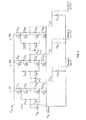
- FIG. 3 illustrates a three-phase power inverter according to one embodiment
- FIG. 4 illustrates a three-level pulse width modulator according to an embodiment of the disclosure
- FIG. 5 illustrates a DC bus ripple feed-forward calculator according to an embodiment of the disclosure
- FIG. 6A illustrates a modulated sinusoidal waveform according to an embodiment of the disclosure
- FIG. 6B illustrates a modulated sinusoidal waveform according to another embodiment of the disclosure.
- FIG. 7 is a flowchart of a method of reducing ripple in a DC bus according to an embodiment of the disclosure.
- FIG. 1 illustrates a system 1 according to one embodiment of the disclosure.
- the system 1 includes a three-phase generator 10 configured to generate voltage outputs having three phases A, B, and C.
- the three-phase generator 10 generates power in three phases, each of which is illustrated as a separate alternating current (AC) sourceAC1, AC2, and AC3.
- AC alternating current
- the generator 10 can include a single rotor and stator and the particular winding arrangement is what is illustrated as separate AC current sources.
- the output voltages from the three-phase generator 10 are input to a three-phase, three-level active rectifier 12.
- the three-phase three-level active rectifier 12 includes a boost inductor stage 102 which also acts as an input filter section.
- Each phase can include its own LRC formed of respective inductors LA1, LA2, LB1, LB2, LC1 and LC2, resistors RA1-RA3, RB1-RB3, and RC1-RC3 and capacitors CA1, CB1, and CC1 to filter the multi-phase AC input currents and to provide a voltage boost operation for the three-phase three-level active rectifier 12. While FIG. 1 illustrates a three-phase generator 10, it is understood that any multi-phase generator is encompassed by embodiments of the present disclosure.
- the three-phase, three-level active rectifier 12 includes a plurality of stages including phase A switching components 121, phase B switching components 122, and phase C switching components 123 corresponding to the plurality of phases A, B, and C, respectively.
- Each stage of switching components 121, 122 and 123 includes a plurality of transistors connected in parallel, source-to-drain.
- the stage corresponding to phase A includes transistors TA1 and TA2
- the stage corresponding to phase B includes transistors TB1 and TB2
- the stage corresponding to phase C includes transistors TC1 and TC2.
- the three-phase, three-level active rectifier 12 may further include a plurality of diodes D1-D18 which may correspond to separate elements or to diode-like inherent properties of an integrated circuit including the transistors TA1, TA2, TB1, TB2, TC1, and TC2.
- the three-phase, three-level active rectifier 12 is controlled by an active rectifier controller 14 to generate a dual direct current (DC) output voltage, Vdc-top and Vdc-bottom. Each bus voltage is half of the full bus voltage from top to bottom.
- the Vdc-top and Vdc-bottom correspond to positive and negative rails which are symmetrical to each other from a common ground, Vdc-mid.
- the active rectifier controller 14 may provide control signals to turn on and off the transistors TA1, TA2, TB1, TB2, TC1, and TC2.
- Outputs at the ends of the stages and a center of the stages between the respective transistors provide the dual DC bus.
- an output connecting a first end of each one of the stages 121, 122, and 123 provides a first DC voltage Vdc_top
- an output connecting a second end of each one of the stages 121, 122, and 123 provides a second DC voltage Vdc_bottom
- an output connecting nodes between each of the pairs of transistors TA1 and TA2, TB1 and TB2 provides a third DC voltage Vdc_mid between the first and second DC voltages Vdc_top and Vdc_bottom.
- Vdc_top corresponds to a positive DC voltage
- Vdc_bottom corresponds to a negative DC voltage
- Vdc_mid corresponds to a DC voltage midway between Vdc_top and Vdc_bottom.
- Vdc_mid corresponds to ground, and in one embodiment, ground has a voltage potential of 0 volts.
- an active rectifier controller 14 controls the gates of the transistors TA1, TA2, TB1, TB2, TC1, and TC2 to generate the dual DC output voltages Vdc_top and Vdc _bottom.
- the system 1 may further include first and second capacitors C1 and C2 connected between Vdc _top, Vdc _mid, and Vdc _bottom, respectively.
- Vdc _top, Vdc _mid, and Vdc _bottom are input to a three-phase, three-level power inverter 16.
- the three-phase, three-level power inverter 16 includes a plurality of stages 161, 162, and 163, corresponding to the respective phases A, B, and C. Each stage includes a plurality of transistors connected in series, source-to-drain.
- the first stage 161 corresponding to phase A includes transistors TA3, TA4, TA5, and TA6;
- the second stage 162 corresponding to phase B includes transistors TB3, TB4, TB5, and TB6;
- the third stage 163 corresponding to phase C includes transistors TC3, TC4, TC5, and TC6.
- the three-phase, three-level power inverter 16 may further include one or more capacitors, such as capacitors CA2, CB2, and CC2, and one or more inductors, such as inductors LA3, LB3, and LC3.
- the gates of the transistors TA3-TA6, TB3-TB6, and TC3-TC6 are controlled by signals 26 from a three-level pulse width modulator (PWM) 18 to generate a three-phase output signal including phases A, B, and C to drive a three-phase AC motor 22.
- PWM pulse width modulator
- FIG. 1 a three-phase, three-level power inverter 16 is illustrated in FIG. 1 , it is understood that a power inverter having any number of stages or levels is encompassed by embodiments of the present disclosure.
- the three-level PWM modulator 18 receives as an input a waveform 24 generated by the DC bus ripple feed-forward calculator 20.
- the three-level PWM 18 includes a triangle waveform generator 181 which generates triangle waveforms 29.
- the waveform 24 from the DC bus ripple feed-forward calculator 20 is applied to the triangle waveforms 29 by a modulated control signal generator 182 to generate the output control signals CTRLTA3-CTRLTA6, CTRLTB3-CTRLTB6, and CTRLTC3-CTRLTC6 to drive the transistors TA3-TA6, TB3-TB6, and TC3-TC6, respectively.
- the triangle waveform generator 181 and modulated control signal generator 182 may comprise one or more of oscillators, filters, rectifiers, and other circuitry and software to generate the triangle waveforms and pulse width modulated control signals 26.
- the waveform 24 is a modulated sinusoidal waveform, the modulation corresponding to ripple detected by the DC bus ripple feed-forward calculator 20, and the modulation being configured to cancel the ripple from the DC bus.
- the DC voltage lines Vdc _top and Vdc _bottom include ripple, such as harmonic ripple coming from the generating power source as well as the rectification, which may cause the DC voltage of the dual DC bus Vdc_top and Vdc_bottom to vary in amplitude up-and-down from its assumed-to-be-a-constant value.
- a modulation is applied to a base sinusoidal waveform (indicated for description purposes by reference numeral 28 in FIG. 6A ) in the DC bus ripple feed-forward calculator 20 to generate a modulated sinusoidal waveform 24 having a modulation to offset the ripple of the DC bus.
- FIGS. 6A and 6B illustrate embodiments of example modulated sinusoidal waveforms 24 and pulse width modulated control signals 26 according to embodiments of the present disclosure.
- the base sinusoidal waveform 28 is illustrated for description purposes, and in FIG. 6B , the base sinusoidal waveform 28 is omitted.
- the pulse width modulated control signals 26 are generated based on a value of the modulated sinusoidal waveform 24 compared to a value of the triangle waveforms 29.
- the modulated control signals 26 are transmitted to the three-phase three-level power inverter 16 to generate a multi-phase AC output signal.
- FIG. 5 illustrates a functional block diagram of the DC bus ripple feed-forward calculator 20 according to an embodiment of the present disclosure.
- the DC bus ripple feed-forward calculator 20 includes a signal input unit 202 to receive input signals corresponding to the first DC voltage Vdc_top, the second DC voltage Vdc_bottom, a controlled average of the first DC voltage Vdc_top, and a controlled average of the second DC voltage Vdc_bottom.
- the controlled averages of the first and second DC voltages Vdc_top and Vdc_bottom may correspond to a base voltage on which a ripple causes voltage variations.
- the input signals are provided to a ripple detection and calculation unit 204 which calculates a ripple of the DC voltages Vdc_top and Vdc_bottom.
- controlled averages of first and second DC voltages Vdc_top and Vdc_bottom are determined to approximate a desired DC voltage having no ripple, and the first and second DC voltages Vdc_top and Vdc_bottom are compared to the controlled averages of the first and second DC voltages Vdc_top and Vdc_bottom.
- the ripple detection and calculation unit 204 may comprise one or more comparison circuits to compare the controlled averages of the first and second DC voltages to the actual first and second DC voltages, and to calculate the ripple of the first and second DC voltages corresponding to the difference between the average DC voltages and the actual DC voltages.
- the calculated ripple may be provided to a ripple cancellation unit 206 which generates a signal 209 to cancel the ripple.
- the ripple cancellation signal for each DC signal Vdc_top and Vdc_bottom has an amplitude opposite the DC signals Vdc_top and Vdc_bottom relative to the controlled averages of the DC voltages Vdc_top and Vdc_bottom.
- the signal 209 to cancel the ripple is combined in the ripple cancellation waveform generator 210 with a base control signal 28 generated by a motor controller 30 to output the modulated waveform 24 having a modulation configured to cancel the ripple caused by the DC voltage lines Vdc_top and Vdc_bottom.
- the signal 209 to cancel the ripple corresponds to the difference between the base control signal 28 and the modulated waveform 24.
- the motor controller 30 may receive motor control signals 32 and feedback and/or feed-forward signals from the motor 22 and may generate the base control signal 28 having a mainly sinusoidal shape, such that the waveform 24 is a modulated sinusoidal waveform 24.
- the ripple cancellation waveform generator 210 may include, for example, an adding circuit to modulate the amplitude of the base waveform generated by the motor controller 30 using a ripple cancellation waveform output from the ripple cancellation unit 206.
- the three-level PWM modulator 18 receives as an input the modulated sinusoidal waveform 24, and outputs pulse width modulated control signals CTRLTA3-CTRLTA6, CTRLTB3-CTRLTB6, and CTRLTC3-CTRLTC6 to control the transistors of the three-phase, three-level power inverter 16. Since the pulse width modulated control signals CTRLTA3-CTRLTA6, CTRLTB3-CTRLTB6, and CTRLTC3-CTRLTC6 are generated based on the modulated sinusoidal waveform 24 that is modulated to reduce or cancel the ripple from the DC bus, the ripple from the DC voltage lines Vdc_top and Vdc_bottom is not passed through to the phase outputs A, B, and C of FIG. 3 , and is not passed through to the motor 22 of FIG. 1 .
- FIG. 7 is a flowchart illustrating a method of compensating ripple according to one embodiment of the present disclosure.
- a ripple in a DC bus is detected and calculated.
- a plurality of DC voltages of a DC bus may be input to a ripple detection and calculation assembly, and the ripple detection and calculation assembly may determine a level of ripple in the plurality of DC voltages.
- the plurality of DC voltages is generated from a multi-phase generator and includes harmonic ripple.
- the level of ripple in DC lines of the DC bus are calculated by comparing voltage levels of the DC lines to predetermined DC voltage levels, such as controlled average DC voltage levels of the DC lines.
- a ripple-cancellation waveform is generated based on the determined level of ripple.
- the ripple-cancellation waveform is a waveform configured to cancel the ripple of the plurality of DC voltages when applied to the plurality of DC voltages.
- a plurality of ripple-calculation waveforms may be generated, each ripple-calculation waveform corresponding to a separate one of the plurality of DC voltages.
- the ripple-cancellation waveform is a waveform having a voltage level such that combining the ripple-cancellation waveform with a waveform of the detected ripple results in a substantially constant DC voltage.
- the ripple-cancellation waveform is applied to a base waveform.
- the base waveform is a sinusoidal waveform
- the ripple-cancellation waveform is applied to the sinusoidal waveform to modulate the amplitude of the sinusoidal waveform.
- the base waveform is a waveform configured to operate a device, such as a motor by applying control signals to the device in a pattern determined by the base waveform.
- pulse width modulated control signals are generated with the sinusoidal waveform modulated by the ripple-cancellation waveform.
- the modulated sinusoidal waveform is provided to a three-level pulse width modulator 18 which generates the pulse width modulated control signals.
- a separate modulated sinusoidal waveform is generated for each output phase of the system 1. For example, in a system 1 such as illustrated in FIG. 1 in which three output phases A, B, and C are generated to control a motor 22, three separate modulated sinusoidal waves may be generated by a DC bus ripple feed-forward calculator 20 and supplied to the three-level PWM modulator 18.
- the three separate modulated sinusoidal waves may then be used to generate separate sets of pulse width modulated control signals to control transistors of a three-phase, three-level power inverter 16 to generate the three output phases A, B, and C of a multi-phase AC voltage in operation 75.
- ripple is detected in a DC bus, a compensation signal is generated and applied to a base waveform, and a modulated waveform based on the combination of the compensation signal and the base waveform is provided to a pulse width modulator to generate pulse width modulation control signals.
- the pulse width modulation control signals may be applied to a multi-level power inverter to generate modulated multi-phase voltages having ripple reduced or eliminated.
- Embodiments of the present disclosure include multi-phase systems and apparatuses including multi-phase generators, rectifiers, power inverters, and pulse width modulators.
- Embodiments of the present disclosure further include methods and processes to reduce or eliminate ripple output from a multi-phase power inverter having as inputs a DC bus which may include ripple.
Landscapes
- Engineering & Computer Science (AREA)
- Power Engineering (AREA)
- Inverter Devices (AREA)
- Air Bags (AREA)
Applications Claiming Priority (1)
| Application Number | Priority Date | Filing Date | Title |
|---|---|---|---|
| US13/453,527 US8982587B2 (en) | 2012-04-23 | 2012-04-23 | Compensating ripple on pulse with modulator outputs |
Publications (3)
| Publication Number | Publication Date |
|---|---|
| EP2658104A2 true EP2658104A2 (fr) | 2013-10-30 |
| EP2658104A3 EP2658104A3 (fr) | 2017-01-04 |
| EP2658104B1 EP2658104B1 (fr) | 2025-09-17 |
Family
ID=48226969
Family Applications (1)
| Application Number | Title | Priority Date | Filing Date |
|---|---|---|---|
| EP13164898.2A Active EP2658104B1 (fr) | 2012-04-23 | 2013-04-23 | Compensation d'ondulation résiduelle |
Country Status (2)
| Country | Link |
|---|---|
| US (1) | US8982587B2 (fr) |
| EP (1) | EP2658104B1 (fr) |
Families Citing this family (17)
| Publication number | Priority date | Publication date | Assignee | Title |
|---|---|---|---|---|
| US8929111B2 (en) * | 2012-10-22 | 2015-01-06 | Hamilton Sundstrand Corporation | System and method for common-mode elimination in a multi-level converter |
| EP2741330A1 (fr) * | 2012-12-06 | 2014-06-11 | Nxp B.V. | Protection contre les décharges électrostatiques |
| US9270168B2 (en) | 2013-03-15 | 2016-02-23 | Hamilton Sundstrand Corporation | Electromagnetic interference (EMI) reduction in multi-level power converter |
| US20140268948A1 (en) * | 2013-03-15 | 2014-09-18 | Hamilton Sundstrand Corporation | Electromagnetic interference (emi) reduction in interleaved power converter |
| US9837893B2 (en) * | 2013-07-31 | 2017-12-05 | Fairchild Korea Semiconductor Ltd. | Charge pump and switch control circuit |
| US9237288B2 (en) * | 2013-12-19 | 2016-01-12 | City University Of Hong Kong | Signal modulating interface for a solid state electronic device |
| CN104038030B (zh) * | 2014-06-04 | 2017-01-04 | 华为技术有限公司 | 一种控制母线纹波的方法、装置和系统 |
| KR20160109137A (ko) * | 2015-03-10 | 2016-09-21 | 엘에스산전 주식회사 | 인버터 시스템 |
| US9840968B2 (en) | 2015-09-16 | 2017-12-12 | Hamilton Sundstrand Corporation | Topologies and methods for turbine engine start inverters |
| US9912266B2 (en) | 2016-08-02 | 2018-03-06 | Otis Elevator Company | Motor torque ripple reduction using DC bus harmonics |
| US10523130B2 (en) * | 2018-01-22 | 2019-12-31 | Hamilton Sundstrand Corporation | Alternate grounding of inverter midpoint for three level switching control |
| JP7154019B2 (ja) * | 2018-03-08 | 2022-10-17 | ナブテスコ株式会社 | Ac-ac電力変換装置 |
| US10574132B2 (en) * | 2018-03-14 | 2020-02-25 | Alpha And Omega Semiconductor (Cayman) Limited | Inductor with bypass switch |
| EP3799282A1 (fr) * | 2019-09-27 | 2021-03-31 | Siemens Aktiengesellschaft | Convertisseur de courant à amortissement actif de la tension d'un circuit intermédiaire |
| US11387859B2 (en) * | 2020-06-29 | 2022-07-12 | Motorola Solutions, Inc. | Method and apparatus for mitigating image interference in a receiver |
| CN115296552B (zh) * | 2022-08-16 | 2024-05-28 | 易事特储能科技有限公司 | 低干扰高效率TL-Boost控制方法 |
| CN115955138B (zh) * | 2022-12-13 | 2025-06-10 | 电子科技大学 | 基于纹波预测的三电平逆变器脉冲延时补偿系统及方法 |
Citations (5)
| Publication number | Priority date | Publication date | Assignee | Title |
|---|---|---|---|---|
| EP0293915A2 (fr) * | 1987-06-03 | 1988-12-07 | Hitachi, Ltd. | Dispositif de commande pour onduleur |
| US5053939A (en) * | 1990-08-27 | 1991-10-01 | Sundstrand Corporation | Control of PWM inverters by pattern development from stored constants relating D.C. link harmonics to output distortion |
| EP0698519A1 (fr) * | 1994-08-25 | 1996-02-28 | Kabushiki Kaisha Toshiba | Dispositif de commande pour une véhicule électrique alimenté à la fois par courant alternatif et par courant continu |
| EP2151916A1 (fr) * | 2007-05-31 | 2010-02-10 | Mitsubishi Electric Corporation | Convertisseur de puissance |
| EP2396882B1 (fr) * | 2009-02-11 | 2014-10-22 | ABB Research Ltd. | Procédé dans un convertisseur à deux niveaux en cascade, dispositif de commande et produits programmes d'ordinateur |
Family Cites Families (8)
| Publication number | Priority date | Publication date | Assignee | Title |
|---|---|---|---|---|
| US5481451A (en) * | 1992-10-30 | 1996-01-02 | Arex Electronics Corporation | AC-to-AC power inverter apparatus functioning without smoothing capacitor, and control method thereof |
| US5664047A (en) * | 1995-08-28 | 1997-09-02 | Iomega Corporation | System for controlling the speed of a motor driven by an unregulated voltage |
| US6154379A (en) * | 1998-07-16 | 2000-11-28 | Tdk Corporation | Electric power conversion device |
| US6850426B2 (en) * | 2002-04-30 | 2005-02-01 | Honeywell International Inc. | Synchronous and bi-directional variable frequency power conversion systems |
| US6838925B1 (en) * | 2003-10-07 | 2005-01-04 | American Power Conversion Corporation | Three level inverter |
| JP3998624B2 (ja) * | 2003-10-09 | 2007-10-31 | Necエレクトロニクス株式会社 | パルス幅変調波形生成方法及び装置 |
| US7193872B2 (en) * | 2005-01-28 | 2007-03-20 | Kasemsan Siri | Solar array inverter with maximum power tracking |
| JP5771429B2 (ja) * | 2010-05-28 | 2015-08-26 | ローム株式会社 | スイッチング電源装置 |
-
2012
- 2012-04-23 US US13/453,527 patent/US8982587B2/en active Active
-
2013
- 2013-04-23 EP EP13164898.2A patent/EP2658104B1/fr active Active
Patent Citations (5)
| Publication number | Priority date | Publication date | Assignee | Title |
|---|---|---|---|---|
| EP0293915A2 (fr) * | 1987-06-03 | 1988-12-07 | Hitachi, Ltd. | Dispositif de commande pour onduleur |
| US5053939A (en) * | 1990-08-27 | 1991-10-01 | Sundstrand Corporation | Control of PWM inverters by pattern development from stored constants relating D.C. link harmonics to output distortion |
| EP0698519A1 (fr) * | 1994-08-25 | 1996-02-28 | Kabushiki Kaisha Toshiba | Dispositif de commande pour une véhicule électrique alimenté à la fois par courant alternatif et par courant continu |
| EP2151916A1 (fr) * | 2007-05-31 | 2010-02-10 | Mitsubishi Electric Corporation | Convertisseur de puissance |
| EP2396882B1 (fr) * | 2009-02-11 | 2014-10-22 | ABB Research Ltd. | Procédé dans un convertisseur à deux niveaux en cascade, dispositif de commande et produits programmes d'ordinateur |
Also Published As
| Publication number | Publication date |
|---|---|
| US8982587B2 (en) | 2015-03-17 |
| EP2658104A3 (fr) | 2017-01-04 |
| US20130279216A1 (en) | 2013-10-24 |
| EP2658104B1 (fr) | 2025-09-17 |
Similar Documents
| Publication | Publication Date | Title |
|---|---|---|
| EP2658104B1 (fr) | Compensation d'ondulation résiduelle | |
| US9780692B2 (en) | Control device of neutral-point-clamped power converter apparatus, and control method of neutral-point-clamped power converter apparatus | |
| EP2395652B1 (fr) | Systèmes et procédés pour réduire les courants en mode commun d'un entraînement CA | |
| EP2528221A2 (fr) | Redresseur actif à phases multiples | |
| US9419542B2 (en) | Inverter device | |
| US8963453B2 (en) | Method and apparatus for synchronization of pulse width modulation | |
| CN110832769B (zh) | 功率转换装置、电动助力转向装置 | |
| JP5512593B2 (ja) | 電力変換装置及びその運転方法 | |
| JPWO1997025766A1 (ja) | 多レベル電力変換装置 | |
| JPH05227796A (ja) | 電力変換器の制御装置 | |
| JP6131360B1 (ja) | 電力変換装置 | |
| KR20160108216A (ko) | 변환 장치 | |
| JP6117039B2 (ja) | 電力変換装置およびエレベーター | |
| KR102441724B1 (ko) | 변환 장치 및 그 제어 방법 | |
| KR101225344B1 (ko) | 전력 변환기, 그 제어 방법 및 다이렉트 매트릭스 컨버터 | |
| JP4755504B2 (ja) | 電力変換装置 | |
| JP6138035B2 (ja) | 電力変換装置及び制御装置 | |
| KR101520899B1 (ko) | 공진효과를 저감시키는 3상 pwm 컨버터 시스템 | |
| JP5190683B2 (ja) | 交流電源装置 | |
| CN115398789A (zh) | 用分离dc链路控制多电平逆变器的方法 | |
| JP7667713B2 (ja) | インバータ装置 | |
| CN115411731B (zh) | 控制装置及控制方法 | |
| JP5894031B2 (ja) | 電力変換装置 | |
| JP2017034805A (ja) | 電力変換装置 | |
| KR101860576B1 (ko) | 인버터 제어장치 |
Legal Events
| Date | Code | Title | Description |
|---|---|---|---|
| PUAI | Public reference made under article 153(3) epc to a published international application that has entered the european phase |
Free format text: ORIGINAL CODE: 0009012 |
|
| AK | Designated contracting states |
Kind code of ref document: A2 Designated state(s): AL AT BE BG CH CY CZ DE DK EE ES FI FR GB GR HR HU IE IS IT LI LT LU LV MC MK MT NL NO PL PT RO RS SE SI SK SM TR |
|
| AX | Request for extension of the european patent |
Extension state: BA ME |
|
| PUAL | Search report despatched |
Free format text: ORIGINAL CODE: 0009013 |
|
| AK | Designated contracting states |
Kind code of ref document: A3 Designated state(s): AL AT BE BG CH CY CZ DE DK EE ES FI FR GB GR HR HU IE IS IT LI LT LU LV MC MK MT NL NO PL PT RO RS SE SI SK SM TR |
|
| AX | Request for extension of the european patent |
Extension state: BA ME |
|
| RIC1 | Information provided on ipc code assigned before grant |
Ipc: H02M 7/487 20070101ALI20161129BHEP Ipc: H02M 1/14 20060101AFI20161129BHEP Ipc: H02M 5/458 20060101ALI20161129BHEP |
|
| STAA | Information on the status of an ep patent application or granted ep patent |
Free format text: STATUS: REQUEST FOR EXAMINATION WAS MADE |
|
| 17P | Request for examination filed |
Effective date: 20170703 |
|
| RBV | Designated contracting states (corrected) |
Designated state(s): AL AT BE BG CH CY CZ DE DK EE ES FI FR GB GR HR HU IE IS IT LI LT LU LV MC MK MT NL NO PL PT RO RS SE SI SK SM TR |
|
| STAA | Information on the status of an ep patent application or granted ep patent |
Free format text: STATUS: EXAMINATION IS IN PROGRESS |
|
| 17Q | First examination report despatched |
Effective date: 20200528 |
|
| REG | Reference to a national code |
Ref country code: DE Ref legal event code: R079 Free format text: PREVIOUS MAIN CLASS: H02M0001140000 Ipc: H02M0007483000 Ref country code: DE Ref legal event code: R079 Ref document number: 602013087050 Country of ref document: DE Free format text: PREVIOUS MAIN CLASS: H02M0001140000 Ipc: H02M0007483000 |
|
| GRAP | Despatch of communication of intention to grant a patent |
Free format text: ORIGINAL CODE: EPIDOSNIGR1 |
|
| STAA | Information on the status of an ep patent application or granted ep patent |
Free format text: STATUS: GRANT OF PATENT IS INTENDED |
|
| RIC1 | Information provided on ipc code assigned before grant |
Ipc: H02M 1/14 20060101ALI20250314BHEP Ipc: H02M 5/458 20060101ALI20250314BHEP Ipc: H02M 7/487 20070101ALI20250314BHEP Ipc: H02M 7/483 20070101AFI20250314BHEP |
|
| INTG | Intention to grant announced |
Effective date: 20250408 |
|
| GRAS | Grant fee paid |
Free format text: ORIGINAL CODE: EPIDOSNIGR3 |
|
| GRAA | (expected) grant |
Free format text: ORIGINAL CODE: 0009210 |
|
| STAA | Information on the status of an ep patent application or granted ep patent |
Free format text: STATUS: THE PATENT HAS BEEN GRANTED |
|
| AK | Designated contracting states |
Kind code of ref document: B1 Designated state(s): AL AT BE BG CH CY CZ DE DK EE ES FI FR GB GR HR HU IE IS IT LI LT LU LV MC MK MT NL NO PL PT RO RS SE SI SK SM TR |
|
| RAP3 | Party data changed (applicant data changed or rights of an application transferred) |
Owner name: HAMILTON SUNDSTRAND CORPORATION |
|
| REG | Reference to a national code |
Ref country code: GB Ref legal event code: FG4D |
|
| REG | Reference to a national code |
Ref country code: CH Ref legal event code: EP |
|
| REG | Reference to a national code |
Ref country code: IE Ref legal event code: FG4D |
|
| REG | Reference to a national code |
Ref country code: DE Ref legal event code: R096 Ref document number: 602013087050 Country of ref document: DE |
|
| PG25 | Lapsed in a contracting state [announced via postgrant information from national office to epo] |
Ref country code: NO Free format text: LAPSE BECAUSE OF FAILURE TO SUBMIT A TRANSLATION OF THE DESCRIPTION OR TO PAY THE FEE WITHIN THE PRESCRIBED TIME-LIMIT Effective date: 20251217 |
|
| REG | Reference to a national code |
Ref country code: LT Ref legal event code: MG9D |
|
| PG25 | Lapsed in a contracting state [announced via postgrant information from national office to epo] |
Ref country code: FI Free format text: LAPSE BECAUSE OF FAILURE TO SUBMIT A TRANSLATION OF THE DESCRIPTION OR TO PAY THE FEE WITHIN THE PRESCRIBED TIME-LIMIT Effective date: 20250917 |
|
| PG25 | Lapsed in a contracting state [announced via postgrant information from national office to epo] |
Ref country code: HR Free format text: LAPSE BECAUSE OF FAILURE TO SUBMIT A TRANSLATION OF THE DESCRIPTION OR TO PAY THE FEE WITHIN THE PRESCRIBED TIME-LIMIT Effective date: 20250917 |
|
| PG25 | Lapsed in a contracting state [announced via postgrant information from national office to epo] |
Ref country code: GR Free format text: LAPSE BECAUSE OF FAILURE TO SUBMIT A TRANSLATION OF THE DESCRIPTION OR TO PAY THE FEE WITHIN THE PRESCRIBED TIME-LIMIT Effective date: 20251218 |
|
| PG25 | Lapsed in a contracting state [announced via postgrant information from national office to epo] |
Ref country code: SE Free format text: LAPSE BECAUSE OF FAILURE TO SUBMIT A TRANSLATION OF THE DESCRIPTION OR TO PAY THE FEE WITHIN THE PRESCRIBED TIME-LIMIT Effective date: 20250917 |
|
| REG | Reference to a national code |
Ref country code: NL Ref legal event code: MP Effective date: 20250917 |
|
| PG25 | Lapsed in a contracting state [announced via postgrant information from national office to epo] |
Ref country code: LV Free format text: LAPSE BECAUSE OF FAILURE TO SUBMIT A TRANSLATION OF THE DESCRIPTION OR TO PAY THE FEE WITHIN THE PRESCRIBED TIME-LIMIT Effective date: 20250917 |
|
| PG25 | Lapsed in a contracting state [announced via postgrant information from national office to epo] |
Ref country code: BG Free format text: LAPSE BECAUSE OF FAILURE TO SUBMIT A TRANSLATION OF THE DESCRIPTION OR TO PAY THE FEE WITHIN THE PRESCRIBED TIME-LIMIT Effective date: 20250917 |
|
| PG25 | Lapsed in a contracting state [announced via postgrant information from national office to epo] |
Ref country code: RS Free format text: LAPSE BECAUSE OF FAILURE TO SUBMIT A TRANSLATION OF THE DESCRIPTION OR TO PAY THE FEE WITHIN THE PRESCRIBED TIME-LIMIT Effective date: 20251217 |
|
| PG25 | Lapsed in a contracting state [announced via postgrant information from national office to epo] |
Ref country code: NL Free format text: LAPSE BECAUSE OF FAILURE TO SUBMIT A TRANSLATION OF THE DESCRIPTION OR TO PAY THE FEE WITHIN THE PRESCRIBED TIME-LIMIT Effective date: 20250917 |
|
| REG | Reference to a national code |
Ref country code: AT Ref legal event code: MK05 Ref document number: 1839246 Country of ref document: AT Kind code of ref document: T Effective date: 20250917 |
|
| PG25 | Lapsed in a contracting state [announced via postgrant information from national office to epo] |
Ref country code: SM Free format text: LAPSE BECAUSE OF FAILURE TO SUBMIT A TRANSLATION OF THE DESCRIPTION OR TO PAY THE FEE WITHIN THE PRESCRIBED TIME-LIMIT Effective date: 20250917 |
|
| PG25 | Lapsed in a contracting state [announced via postgrant information from national office to epo] |
Ref country code: ES Free format text: LAPSE BECAUSE OF FAILURE TO SUBMIT A TRANSLATION OF THE DESCRIPTION OR TO PAY THE FEE WITHIN THE PRESCRIBED TIME-LIMIT Effective date: 20250917 |
|
| PG25 | Lapsed in a contracting state [announced via postgrant information from national office to epo] |
Ref country code: AT Free format text: LAPSE BECAUSE OF FAILURE TO SUBMIT A TRANSLATION OF THE DESCRIPTION OR TO PAY THE FEE WITHIN THE PRESCRIBED TIME-LIMIT Effective date: 20250917 |
|
| PG25 | Lapsed in a contracting state [announced via postgrant information from national office to epo] |
Ref country code: IT Free format text: LAPSE BECAUSE OF FAILURE TO SUBMIT A TRANSLATION OF THE DESCRIPTION OR TO PAY THE FEE WITHIN THE PRESCRIBED TIME-LIMIT Effective date: 20250917 |
|
| PG25 | Lapsed in a contracting state [announced via postgrant information from national office to epo] |
Ref country code: IS Free format text: LAPSE BECAUSE OF FAILURE TO SUBMIT A TRANSLATION OF THE DESCRIPTION OR TO PAY THE FEE WITHIN THE PRESCRIBED TIME-LIMIT Effective date: 20260117 |
|
| PGFP | Annual fee paid to national office [announced via postgrant information from national office to epo] |
Ref country code: FR Payment date: 20260320 Year of fee payment: 14 |
|
| PG25 | Lapsed in a contracting state [announced via postgrant information from national office to epo] |
Ref country code: PT Free format text: LAPSE BECAUSE OF FAILURE TO SUBMIT A TRANSLATION OF THE DESCRIPTION OR TO PAY THE FEE WITHIN THE PRESCRIBED TIME-LIMIT Effective date: 20260119 Ref country code: CZ Free format text: LAPSE BECAUSE OF FAILURE TO SUBMIT A TRANSLATION OF THE DESCRIPTION OR TO PAY THE FEE WITHIN THE PRESCRIBED TIME-LIMIT Effective date: 20250917 |
|
| PG25 | Lapsed in a contracting state [announced via postgrant information from national office to epo] |
Ref country code: PL Free format text: LAPSE BECAUSE OF FAILURE TO SUBMIT A TRANSLATION OF THE DESCRIPTION OR TO PAY THE FEE WITHIN THE PRESCRIBED TIME-LIMIT Effective date: 20250917 |
|
| PG25 | Lapsed in a contracting state [announced via postgrant information from national office to epo] |
Ref country code: EE Free format text: LAPSE BECAUSE OF FAILURE TO SUBMIT A TRANSLATION OF THE DESCRIPTION OR TO PAY THE FEE WITHIN THE PRESCRIBED TIME-LIMIT Effective date: 20250917 Ref country code: SK Free format text: LAPSE BECAUSE OF FAILURE TO SUBMIT A TRANSLATION OF THE DESCRIPTION OR TO PAY THE FEE WITHIN THE PRESCRIBED TIME-LIMIT Effective date: 20250917 |