EP2660656A1 - Appareil d'alignement sur face arrière et procédé - Google Patents
Appareil d'alignement sur face arrière et procédé Download PDFInfo
- Publication number
- EP2660656A1 EP2660656A1 EP11852338.0A EP11852338A EP2660656A1 EP 2660656 A1 EP2660656 A1 EP 2660656A1 EP 11852338 A EP11852338 A EP 11852338A EP 2660656 A1 EP2660656 A1 EP 2660656A1
- Authority
- EP
- European Patent Office
- Prior art keywords
- alignment mark
- workpiece stage
- imaging
- reference plate
- backside
- Prior art date
- Legal status (The legal status is an assumption and is not a legal conclusion. Google has not performed a legal analysis and makes no representation as to the accuracy of the status listed.)
- Granted
Links
Images




Classifications
-
- G—PHYSICS
- G03—PHOTOGRAPHY; CINEMATOGRAPHY; ANALOGOUS TECHNIQUES USING WAVES OTHER THAN OPTICAL WAVES; ELECTROGRAPHY; HOLOGRAPHY
- G03F—PHOTOMECHANICAL PRODUCTION OF TEXTURED OR PATTERNED SURFACES, e.g. FOR PRINTING, FOR PROCESSING OF SEMICONDUCTOR DEVICES; MATERIALS THEREFOR; ORIGINALS THEREFOR; APPARATUS SPECIALLY ADAPTED THEREFOR
- G03F9/00—Registration or positioning of originals, masks, frames, photographic sheets or textured or patterned surfaces, e.g. automatically
- G03F9/70—Registration or positioning of originals, masks, frames, photographic sheets or textured or patterned surfaces, e.g. automatically for microlithography
- G03F9/7003—Alignment type or strategy, e.g. leveling, global alignment
- G03F9/7007—Alignment other than original with workpiece
- G03F9/7015—Reference, i.e. alignment of original or workpiece with respect to a reference not on the original or workpiece
-
- G—PHYSICS
- G01—MEASURING; TESTING
- G01B—MEASURING LENGTH, THICKNESS OR SIMILAR LINEAR DIMENSIONS; MEASURING ANGLES; MEASURING AREAS; MEASURING IRREGULARITIES OF SURFACES OR CONTOURS
- G01B11/00—Measuring arrangements characterised by the use of optical techniques
- G01B11/26—Measuring arrangements characterised by the use of optical techniques for measuring angles or tapers; for testing the alignment of axes
-
- G—PHYSICS
- G01—MEASURING; TESTING
- G01N—INVESTIGATING OR ANALYSING MATERIALS BY DETERMINING THEIR CHEMICAL OR PHYSICAL PROPERTIES
- G01N21/00—Investigating or analysing materials by the use of optical means, i.e. using sub-millimetre waves, infrared, visible or ultraviolet light
- G01N21/17—Systems in which incident light is modified in accordance with the properties of the material investigated
- G01N21/25—Colour; Spectral properties, i.e. comparison of effect of material on the light at two or more different wavelengths or wavelength bands
- G01N21/31—Investigating relative effect of material at wavelengths characteristic of specific elements or molecules, e.g. atomic absorption spectrometry
- G01N21/35—Investigating relative effect of material at wavelengths characteristic of specific elements or molecules, e.g. atomic absorption spectrometry using infrared light
-
- G—PHYSICS
- G03—PHOTOGRAPHY; CINEMATOGRAPHY; ANALOGOUS TECHNIQUES USING WAVES OTHER THAN OPTICAL WAVES; ELECTROGRAPHY; HOLOGRAPHY
- G03F—PHOTOMECHANICAL PRODUCTION OF TEXTURED OR PATTERNED SURFACES, e.g. FOR PRINTING, FOR PROCESSING OF SEMICONDUCTOR DEVICES; MATERIALS THEREFOR; ORIGINALS THEREFOR; APPARATUS SPECIALLY ADAPTED THEREFOR
- G03F9/00—Registration or positioning of originals, masks, frames, photographic sheets or textured or patterned surfaces, e.g. automatically
- G03F9/70—Registration or positioning of originals, masks, frames, photographic sheets or textured or patterned surfaces, e.g. automatically for microlithography
- G03F9/7073—Alignment marks and their environment
- G03F9/7084—Position of mark on substrate, i.e. position in (x, y, z) of mark, e.g. buried or resist covered mark, mark on rearside, at the substrate edge, in the circuit area, latent image mark, marks in plural levels
-
- G—PHYSICS
- G03—PHOTOGRAPHY; CINEMATOGRAPHY; ANALOGOUS TECHNIQUES USING WAVES OTHER THAN OPTICAL WAVES; ELECTROGRAPHY; HOLOGRAPHY
- G03F—PHOTOMECHANICAL PRODUCTION OF TEXTURED OR PATTERNED SURFACES, e.g. FOR PRINTING, FOR PROCESSING OF SEMICONDUCTOR DEVICES; MATERIALS THEREFOR; ORIGINALS THEREFOR; APPARATUS SPECIALLY ADAPTED THEREFOR
- G03F9/00—Registration or positioning of originals, masks, frames, photographic sheets or textured or patterned surfaces, e.g. automatically
- G03F9/70—Registration or positioning of originals, masks, frames, photographic sheets or textured or patterned surfaces, e.g. automatically for microlithography
- G03F9/7088—Alignment mark detection, e.g. TTR, TTL, off-axis detection, array detector, video detection
Definitions
- This invention relates in general to integrated circuit manufacturing devices, and more particularly, to an apparatus and method for backside alignment in a semiconductor lithography device.
- MCP multi-chip packaging
- TSV bonding is considered as one of the most potential and promising 3D packaging methods, because it has many advantages such as a smaller length and a higher density of bonding leads, a smaller package area and non-significant increase of package cost with the increase in the number of packaged chips, compared with the relatively conventional wire bonding method.
- fine vias are formed through each semiconductor silicon chip, namely extending from the frontside to the backside of the semiconductor silicon chip, and then the stacked silicon chips are electrically connected to one another.
- bonding leads arranged between the silicon chips can be greatly shortened and a final device can be significantly improved in terms of volume, performance and signal access and transmission speed.
- relevant semiconductor lithography devices are required to be equipped with a backside alignment apparatus which uses a pattern formed on a frontside (or a top surface) of the wafer as a reference mark for a backside (or a bottom surface) of the wafer to determine a deviation between positions of the pattern formed on the frontside and a pattern to be exposed on the backside of the wafer.
- a backside alignment apparatus which uses a pattern formed on a frontside (or a top surface) of the wafer as a reference mark for a backside (or a bottom surface) of the wafer to determine a deviation between positions of the pattern formed on the frontside and a pattern to be exposed on the backside of the wafer.
- a visual light measuring method a light-path turning device and an imaging device are arranged on opposite sides under a wafer stage for illuminating and imaging a backside reference mark of the wafer using a visual light.
- a backside reference mark of the wafer is illuminated and imaged by using the wafer penetrating property of the infrared light.
- US patent Nos. 6525805B and 6768539B respectively disclose a typical backside alignment apparatus, which uses an off-axis alignment apparatus to achieve wafer backside alignment with visual light measuring method.
- each backside alignment mark corresponding to a set of illumination devices, it is complicated and expensive to assemble these illumination devices together.
- its design of arranging the illumination devices under a wafer stage leads to a high complexity and processing cost in structure design of the wafer stage.
- the apparatus has poor process adaptation.
- US patent No. 6525805B also discloses a backside alignment apparatus using infrared light measuring method.
- near-infrared light sources are arranged at different positions within the wafer stage for illuminating backside alignment marks of the wafer, and a near-infrared imaging device is disposed above the wafer for imaging the alignment marks.
- illumination devices for illuminating backside marks of the wafer are arranged within the wafer stage, the structure design and assembly of the wafer stage are complicated and may have a high processing cost; moreover, the structure design may be restricted by the overall alignment accuracy of the wafer and space size of the wafer stage.
- alignment marks need to be formed at predetermined positions to co-work with the backside mark illumination devices, thus increasing process steps and complexity and leading to a poor process adaptation.
- the present invention overcomes the foregoing drawbacks of the conventional art by presenting a backside alignment apparatus and method, which are simpler in configuration and able to overall reduce design and processing complexities for integrated circuit fabrication equipment.
- the present invention discloses a backside alignment apparatus for determining a relationship between relative positions of a substrate and a workpiece stage.
- the backside alignment apparatus comprises: a radiation source for emanating infrared light; a workpiece stage assembly for supporting and moving the substrate; an imaging apparatus for detecting alignment marks and calculating positions of the alignment marks; and a reference plate assembly for setting up a relationship between position coordinates of the imaging apparatus and the workpiece stage assembly.
- illumination and alignment of multiple alignment marks including both a reference plate alignment mark and backside alignment mark(s), can be achieved only using one set of radiation source and imaging apparatus.
- the workpiece stage assembly may include at least three apertures for the infrared light to pass through.
- the backside alignment apparatus may further comprise an illumination apparatus.
- the illumination apparatus may be disposed above the workpiece stage assembly, and in this case the illumination apparatus includes an optical fiber and an illumination lens group. Moreover, the illumination apparatus may also be disposed under the workpiece stage assembly, and in this case it includes an optical fiber, an illumination lens group and an illuminating reflection mirror.
- the workpiece stage assembly may include a workpiece stage and a base under the workpiece stage, and the workpiece stage is able to move in at least three degrees of freedom with respect to the base.
- the workpiece stage may further include a chuck which is made of glass or a material with a high transmittance for infrared light and disposed on the workpiece stage.
- the at least three apertures include one base aperture and two workpiece stage apertures.
- the imaging apparatus may be disposed right above one of the apertures in the workpiece stage assembly, and in this case the imaging apparatus includes an imaging lens group, an imaging detector and an image processing system. Moreover, the imaging apparatus may also be disposed right under one of the apertures in the workpiece stage assembly, and in this case it includes an imaging lens group, an illuminating reflection mirror, an imaging detector and an image processing system.
- the imaging detector may be a charge-coupled device (CCD) detector, a complementary metal-oxide-semiconductor (CMOS) detector, or an indium-gallium-arsenide (InGaAs) detector.
- the reference plate assembly may include a reference plate, a reference plate alignment mark and a frame. Additionally, the reference plate alignment mark is disposed on a bottom surface of the reference plate. Moreover, the reference plate is fixed on the frame and the reference plate alignment mark is leveling with the backside alignment marks.
- the frame is formed of glass or a material with a high transmittance for infrared light. The reference plate assembly may be disposed either on the workpiece stage or on the chuck.
- positions, the number and sizes of apertures formed in the workpiece stage may depend on alignment accuracy and the size of a single chip.
- the present invention also discloses a backside alignment method for determining a relationship between relative positions of the substrate and the workpiece stage.
- the method comprises: a) moving the reference plate alignment mark into an imaging field of the imaging apparatus and acquiring a first position information indicating a relationship between position coordinates of the imaging apparatus and the workpiece stage; b) moving each of the at least one backside alignment mark into the imaging field of the imaging apparatus and acquiring a second position information indicating a relationship between position coordinates of the substrate and the imaging apparatus; and c) determining a relationship between positions of the substrate and the workpiece stage based on the first and second position information.
- the step a) may include: a1) moving the workpiece stage to a desired location such that the reference plate alignment mark is located within an imaging field of the imaging apparatus; a2) determining, using the image processing system, whether the reference plate alignment mark is within the imaging detector, and if the reference plate alignment mark is within the imaging detector, then calculating a position of the reference plate alignment mark on a target plane of the imaging detector using the image processing system and recording a horizontal position of the workpiece stage; and a3) if the reference plate alignment mark is not within the imaging detector, then moving the workpiece stage, by a predetermined distance, into a next search location; if the next search location is out of a predetermined search range, then ending the search; and if the reference plate alignment mark is captured within the predetermined search range, then repeating the step a2).
- the step b) may include: b1) moving the workpiece stage to a desired location such that one of the at least one backside alignment mark is located within an imaging field of the imaging apparatus; b2) determining, using the image processing system, whether the backside alignment mark is within the imaging detector, and if the backside alignment mark is within the imaging detector, then calculating a position of the backside alignment mark on a target plane of the imaging detector using the image processing system and recording a horizontal position of the workpiece stage; b3) if the backside alignment mark is not within the imaging detector, then moving the workpiece stage, by a predetermined distance, into a next search location; if the next search location is out of a predetermined search range, then ending the search; and if the backside alignment mark is captured within the predetermined search range, then repeating the step b2); and determining whether positions, on a target plane of the imaging detector, of all of the at least one backside alignment mark have been calculated, if not, then repeating the steps b1), b2)
- the step c) may include: c1) calculating a relationship between position coordinates of the imaging apparatus and the workpiece stage; c2) calculating a relationship between position coordinates of the substrate and the imaging apparatus; and c3) obtaining a relationship between relative positions of the substrate and the workpiece stage.
- the present invention has differences with and advantages over the prior art as follows: as only one set of illumination apparatus is used, complexity in the design and assembly of illumination apparatus can be reduced and the development costs can be hence lowered; as the illumination apparatus can be disposed within, above or under the marble workpiece stage, coupling between physical interfaces of the illumination apparatus and the workpiece stage assembly can be reduced; also, complexity in the structure design and assembly of the workpiece stage, and processing cost of the workpiece stage can be lowered; and the enabling of moving the workpiece stage to search a backside alignment mark in a certain range when it is not found within an imaging field of the image apparatus can improve the process adaptation of the backside alignment apparatus to the backside alignment marks.
- the present invention provides a backside alignment apparatus and method for use in integrated circuit fabrication equipments.
- a schematic diagram illustrating such a backside alignment apparatus is shown in FIG.1 , wherein 5 is a projection objective of an integrated circuit fabrication equipment, which may be a refractive projection objective, a reflective projection objective, or a catadioptric projection objective according to the type of the device being produced; 1 is an illumination apparatus of the backside alignment apparatus according to the present invention, which is configured to provide infrared light illumination; and 6 is a substrate which may be made of silicon, glass or other materials according to the type of device being produced. The substrate 6 is disposed on a workpiece stage assembly 2 which can move in at least three degrees of freedom.
- Infrared light emanated from the illumination apparatus 1 passes through both the workpiece stage assembly 2 and a backside alignment mark 20 and enters an imaging apparatus 3.
- a reference plate assembly 4 is provided for setting up a relationship between position coordinates of the imaging apparatus 3 and the workpiece stage assembly 2.
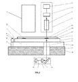
- FIG.2 is a schematic illustration of the backside alignment apparatus according to a first embodiment of the present invention.
- the backside alignment apparatus comprises: an illumination apparatus 1, a workpiece stage assembly 2, an imaging apparatus 3, and a reference plate assembly 4 configured to determine a relationship between positions of a substrate 6 and the workpiece stage assembly 2 by using backside alignment mark(s) 20 formed on the substrate 6.
- the illumination apparatus 1 successively includes an infrared light source 10, an infrared illumination optical fiber 11, an illumination lens group 13 and an illuminating reflection mirror 14, and is configured to provide uniform illumination for a reference plate alignment mark 41 and backside alignment mark(s) 20 of the substrate 6.
- the illumination apparatus 1 may have a structure of a Kohler illumination system. Details about the Kohler illumination system can be obtained by referring to the prior art.
- the workpiece stage assembly 2 at least includes a workpiece stage 24 with multiple degrees of freedom and a marble base 26.
- the workpiece stage 24 with multiple degrees of freedom can move in at least three degrees of freedom, and more preferably, it can move in six degrees of freedom.
- the six degree-of-freedom workpiece stage 24 is configured mainly to support the substrate 6 and enable the substrate 6 to move in six degrees of freedom.
- the six degree-of-freedom workpiece stage 24 may be disposed on the marble base 26.
- the substrate 6 is a silicon substrate as an example and the backside alignment marks 20 are formed on the substrate 6.
- the substrate 6 is typically disposed on the workpiece stage 24 using a chuck 22 which is arranged at the same level with the backside alignment marks 20 and mounted on a top surface of the workpiece stage 24.
- the chuck 22 may be formed of glass or a material with a high transmittance for infrared light.
- the six degree-of-freedom workpiece stage 24 may include two or more workpiece stage apertures 23 formed in it, including one workpiece stage aperture 23 formed right under the reference plate assembly 4 and the rest of the workpiece stage apertures 23 each formed right under a corresponding backside alignment mark 20, thereby allowing infrared light emanated from the illumination apparatus 1 to pass through the workpiece stage apertures 23 and the chuck 22 and uniformly illuminate the backside alignment mark(s) 20 and the reference plate alignment mark 41. Positions, the number and sizes of the workpiece stage apertures 23 are dependent on alignment accuracy and the size of a single chip.
- the marble base 26 may also include a marble aperture 25, i.e. a base aperture for allowing infrared light emanated from the illumination apparatus 1 to pass through the marble base 26.
- the marble aperture 25 is positioned right above the illumination apparatus 1 and right under the imaging apparatus 3 and size of the marble aperture 25 is dependent both on the size of an illumination field of the illumination apparatus 1 and the size of a search range for the backside alignment mark(s) 20.
- the reference plate assembly 4 may include a reference plate 40, the reference plate alignment mark 41 and a reference plate frame 42 and is configured to set up a relationship between position coordinates of the imaging apparatus and the workpiece stage.
- the reference plate alignment mark 41 is positioned on a bottom surface of the reference plate 40 and arranged at the same level with the backside alignment mark(s) 20.
- the reference plate 40 may be fixed on the frame 42 and the frame 42 may be formed of glass or a material with a high transmittance for infrared light for allowing the infrared light emanated from the illumination apparatus 1 to pass through the frame 42 and illuminate the reference plate alignment mark 41.
- the reference plate assembly 4 may be either fixed on the six degree-of-freedom workpiece stage 24 or directly disposed on the chuck 22, such that its position in each of the six degrees of freedom can be adjusted according to the movement of the workpiece stage 24. In contrast, as the illumination apparatus 1 is disposed under the workpiece stage assembly 2, its position will not be affected by movement of the workpiece stage 24.
- the imaging apparatus 3 may include an infrared imaging lens group 31, an infrared imaging detector 32 and an image processing system 33 and is configured to form clear images of the backside alignment mark(s) 20 and the reference plate alignment mark 41 on a target plane of the infrared imaging detector 32 and calculate positions of these alignment marks. Additionally, the infrared imaging detector 32 is configured to receive images of the reference plate alignment mark 41 and the backside alignment mark(s) 20 generated by the infrared imaging lens group 31.
- the infrared imaging detector 32 may be a charge-coupled device (CCD) detector, a complementary metal-oxide-semiconductor (CMOS) detector, or an indium-gallium-arsenide (InGaAs) detector.
- CCD charge-coupled device
- CMOS complementary metal-oxide-semiconductor
- InGaAs indium-gallium-arsenide
- infrared light emitted from the infrared light source 10 successively passes through the infrared illumination optical fiber 11, the illumination lens group 13, the illuminating reflection mirror 14, the marble aperture 25, the workpiece stage aperture 23 and the chuck 22, reaches the reference plate alignment mark 41 or a backside alignment mark 20 and thus uniformly illuminates the mark.
- a backside alignment imaging process may start from the reference plate alignment mark 41 or a backside alignment mark 20, successively pass through the reference plate 40 or substrate 6, the infrared imaging lens group 31, the infrared imaging detector 32 and reach the image processing system 33.
- clear images of the reference plate alignment mark 41 and/or the backside alignment mark(s) 20 can be formed on the infrared imaging detector 32, and the image processing system 33 can acquire positions of the reference plate alignment mark 41 and/or the backside alignment mark(s) 20 on the target plane of the infrared imaging detector 32.
- FIG.3 schematically illustrates the configuration of an illumination apparatus of the backside alignment apparatus of the present invention.
- the reference plate assembly 4 is arranged at a left upper corner of the six degree-of-freedom workpiece stage 24.
- the reference plate assembly 4 may be arranged at any corner of the workpiece stage 24.
- the reference plate assembly 4 may be directed mounted on the chuck 22.
- the reference plate alignment mark 41 and the backside alignment marks 20 are illustrated as crosses "+" in the figures, persons skilled in the art will recognize that in practical operations different marks can also be used as the reference plate alignment mark 41 or the backside alignment marks 20 according to different alignment accuracies and requirements.
- each of the workpiece stage apertures 23 has a size that is greater than both an illumination field and a search range associated with the reference plate alignment mark 41 and the backside alignment marks 20.
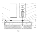
- FIG.4 is a detailed schematic diagram illustrating a backside alignment apparatus according to a second embodiment of the present invention.
- an infrared light source 25 for uniformly illuminating the reference plate alignment mark 41 and the backside alignment mark(s) 20 is embedded within the marble workpiece stage as a replacement of the illumination apparatus 1 of the first embodiment.
- the backside alignment apparatus in this embodiment uses a much smaller number of optical members and thus has a simpler structure and a lower cost.
- FIG.5 is a detailed schematic diagram illustrating a backside alignment apparatus according to a third embodiment of the present invention.
- a backside alignment apparatus comprises: an illumination apparatus 1, a workpiece stage assembly 2, an imaging apparatus 3, and a reference plate assembly 4 configured to determine a relationship between positions of a substrate 6 and the workpiece stage assembly 2 by using backside alignment mark(s) 20 formed on the substrate 6.
- the illumination apparatus 1 may be disposed above the substrate 6 whilst the imaging apparatus 3 is disposed under the substrate 6. Additionally, the illumination apparatus 1 may successively include an infrared light source 10, an infrared illumination optical fiber 11 and an illumination lens group 13, and is configured to uniformly illuminate a reference plate alignment mark 41 and the backside alignment mark(s) 20.
- the illumination apparatus 1 can be structurally similar to a Kohler illumination system.
- the imaging apparatus 3 may include the backside alignment mark(s) 20, workpiece stage apertures 23, a marble aperture 25, an infrared imaging lens group 31, an infrared reflection mirror 34, an infrared imaging detector 32 and an image processing system 33, and is configured to form clear images of the backside alignment mark(s) 20 and the reference plate alignment mark 41 on a target plane of the infrared imaging detector 32 and calculate positions of these alignment marks.
- the present invention also discloses a backside alignment method, comprising: moving the reference plate alignment mark 41 into an imaging field of the imaging apparatus 3 to set up a relationship between position coordinates of the imaging apparatus 3 and the workpiece stage assembly 2; moving each of the backside alignment marks 20 into the imaging field to set up a relationship between position coordinates of the substrate 6 and the imaging apparatus 3; and obtaining the relationship between positions of the substrate 6 and the workpiece stage assembly 2 based on the above two position coordinate relationships.
- FIG.6 is a flow chart of this method which may include the steps of:
- the present invention has differences with and advantages over the conventional art as follows: as only one set of illumination apparatus is used, complexity in the design and assembly of illumination apparatus can be reduced and the development costs can be hence lowered; as the illumination apparatus can be disposed within, above or under the marble workpiece stage, coupling between physical interfaces of the illumination apparatus and the workpiece stage assembly can be reduced; also, complexity in the structure design and assembly of the workpiece stage, and processing cost of the workpiece stage can be lowered; and the enabling of moving the workpiece stage to search a backside alignment mark in a certain range when it is not found within an imaging field of the image apparatus can improve the process adaptation of the backside alignment apparatus to the backside alignment marks.
Landscapes
- Physics & Mathematics (AREA)
- General Physics & Mathematics (AREA)
- Spectroscopy & Molecular Physics (AREA)
- Health & Medical Sciences (AREA)
- Life Sciences & Earth Sciences (AREA)
- Chemical & Material Sciences (AREA)
- Analytical Chemistry (AREA)
- Biochemistry (AREA)
- General Health & Medical Sciences (AREA)
- Immunology (AREA)
- Pathology (AREA)
- Engineering & Computer Science (AREA)
- Multimedia (AREA)
- Container, Conveyance, Adherence, Positioning, Of Wafer (AREA)
- Exposure And Positioning Against Photoresist Photosensitive Materials (AREA)
- Exposure Of Semiconductors, Excluding Electron Or Ion Beam Exposure (AREA)
Applications Claiming Priority (2)
| Application Number | Priority Date | Filing Date | Title |
|---|---|---|---|
| CN201010619055.2A CN102540781B (zh) | 2010-12-28 | 2010-12-28 | 一种背面对准装置及方法 |
| PCT/CN2011/084264 WO2012089043A1 (fr) | 2010-12-28 | 2011-12-20 | Appareil d'alignement sur face arrière et procédé |
Publications (3)
| Publication Number | Publication Date |
|---|---|
| EP2660656A1 true EP2660656A1 (fr) | 2013-11-06 |
| EP2660656A4 EP2660656A4 (fr) | 2015-01-07 |
| EP2660656B1 EP2660656B1 (fr) | 2016-03-09 |
Family
ID=46347945
Family Applications (1)
| Application Number | Title | Priority Date | Filing Date |
|---|---|---|---|
| EP11852338.0A Active EP2660656B1 (fr) | 2010-12-28 | 2011-12-20 | Appareil d'alignement sur face arrière et procédé |
Country Status (5)
| Country | Link |
|---|---|
| US (1) | US9188434B2 (fr) |
| EP (1) | EP2660656B1 (fr) |
| CN (1) | CN102540781B (fr) |
| TW (1) | TW201236103A (fr) |
| WO (1) | WO2012089043A1 (fr) |
Cited By (1)
| Publication number | Priority date | Publication date | Assignee | Title |
|---|---|---|---|---|
| WO2023073232A1 (fr) * | 2021-11-01 | 2023-05-04 | Esko-Graphics Imaging Gmbh | Systèmes et procédés pour le marquage persistant de plaques flexo avec des microstructures et des plaques isolées marquées avec celles-ci |
Families Citing this family (24)
| Publication number | Priority date | Publication date | Assignee | Title |
|---|---|---|---|---|
| US9041919B2 (en) * | 2013-02-18 | 2015-05-26 | Globalfoundries Inc. | Infrared-based metrology for detection of stress and defects around through silicon vias |
| CN104022060A (zh) * | 2013-03-01 | 2014-09-03 | 中芯国际集成电路制造(上海)有限公司 | 晶圆背面对准的方法 |
| CN104155850B (zh) * | 2013-05-13 | 2017-06-27 | 上海微电子装备有限公司 | 用于光刻设备的正面与背面对准测量装置 |
| TWI544567B (zh) * | 2013-06-27 | 2016-08-01 | 先進科技新加坡有限公司 | 使用成像設備以調整半導體元件的處理設備的裝置和方法 |
| CN104749158B (zh) | 2013-12-27 | 2020-12-11 | 同方威视技术股份有限公司 | 珠宝玉石鉴定方法及装置 |
| CN105277131B (zh) * | 2014-05-26 | 2020-11-20 | 上海微电子装备(集团)股份有限公司 | 三维孔结构的测量装置与测量方法 |
| JP6465591B2 (ja) * | 2014-08-27 | 2019-02-06 | 株式会社オーク製作所 | 描画装置 |
| CN105807578A (zh) * | 2014-12-29 | 2016-07-27 | 上海微电子装备有限公司 | 一种背面对准测量装置及方法 |
| US20170138820A1 (en) * | 2015-11-16 | 2017-05-18 | General Electric Company | Systems and methods for monitoring components |
| US12057332B2 (en) * | 2016-07-12 | 2024-08-06 | Ayar Labs, Inc. | Wafer-level etching methods for planar photonics circuits and devices |
| JP6742272B2 (ja) * | 2017-05-16 | 2020-08-19 | 三菱電機株式会社 | ウェハ異常箇所検出用装置およびウェハ異常箇所特定方法 |
| US10381404B2 (en) | 2017-08-07 | 2019-08-13 | Globalfoundries Singapore Pte. Ltd. | Integrated circuits with memory cells and methods for producing the same |
| JP6980562B2 (ja) * | 2018-02-28 | 2021-12-15 | キヤノン株式会社 | パターン形成装置、アライメントマークの検出方法及びパターン形成方法 |
| CN110504203B (zh) * | 2018-05-18 | 2024-11-22 | 上海微电子装备(集团)股份有限公司 | 一种工作台及背面对准装置 |
| CN110246771B (zh) * | 2019-06-18 | 2021-06-15 | 武汉新芯集成电路制造有限公司 | 一种晶圆键合的设备及方法 |
| CN110600414A (zh) * | 2019-08-01 | 2019-12-20 | 中国科学院微电子研究所 | 晶圆异构对准方法及装置 |
| CN112018002A (zh) * | 2020-08-25 | 2020-12-01 | 武汉新芯集成电路制造有限公司 | 晶圆键合设备及晶圆键合的方法 |
| TWI794734B (zh) * | 2021-01-29 | 2023-03-01 | 川寶科技股份有限公司 | 決定基板之轉向的方法與曝光機台 |
| CN113791524A (zh) * | 2021-09-30 | 2021-12-14 | 深圳迈塔兰斯科技有限公司 | 用于超表面加工的光刻系统及方法 |
| DE102022119035A1 (de) * | 2022-07-28 | 2024-02-08 | 4Jet Microtech Gmbh | Detektionsaufbau |
| CN115632018A (zh) * | 2022-09-27 | 2023-01-20 | 北京华卓精科科技股份有限公司 | 晶圆对准方法及对准装置 |
| US12222659B2 (en) * | 2023-01-18 | 2025-02-11 | Applied Materials, Inc. | Metrology system for packaging applications |
| TWI875293B (zh) * | 2023-11-07 | 2025-03-01 | 由田新技股份有限公司 | 輔助標記產生方法、工件對準方法、及工件對準系統 |
| JP2026036495A (ja) * | 2024-08-20 | 2026-03-05 | 株式会社Screenホールディングス | 基板接合装置 |
Family Cites Families (14)
| Publication number | Priority date | Publication date | Assignee | Title |
|---|---|---|---|---|
| US4452526A (en) * | 1980-02-29 | 1984-06-05 | Optimetrix Corporation | Step-and-repeat projection alignment and exposure system with auxiliary optical unit |
| US4475122A (en) * | 1981-11-09 | 1984-10-02 | Tre Semiconductor Equipment Corporation | Automatic wafer alignment technique |
| US5843831A (en) * | 1997-01-13 | 1998-12-01 | Taiwan Semiconductor Manufacturing Company, Ltd. | Process independent alignment system |
| TW406323B (en) * | 1998-08-20 | 2000-09-21 | United Microelectronics Corp | Method for wafer alignment and the apparatus of the same |
| JP2000299276A (ja) * | 1999-04-15 | 2000-10-24 | Nikon Corp | 露光装置 |
| US6676878B2 (en) * | 2001-01-31 | 2004-01-13 | Electro Scientific Industries, Inc. | Laser segmented cutting |
| KR100579603B1 (ko) | 2001-01-15 | 2006-05-12 | 에이에스엠엘 네델란즈 비.브이. | 리소그래피 장치 |
| US6525805B2 (en) * | 2001-05-14 | 2003-02-25 | Ultratech Stepper, Inc. | Backside alignment system and method |
| US7365848B2 (en) * | 2004-12-01 | 2008-04-29 | Asml Holding N.V. | System and method using visible and infrared light to align and measure alignment patterns on multiple layers |
| US7751067B1 (en) * | 2007-05-24 | 2010-07-06 | Ultratech, Inc. | Substrate-alignment using detector of substrate material |
| CN101685275A (zh) * | 2008-09-25 | 2010-03-31 | 上海华虹Nec电子有限公司 | 对准标记及制作方法以及其探测装置 |
| CN101382743B (zh) | 2008-10-27 | 2011-12-21 | 上海微电子装备有限公司 | 同轴双面位置对准系统及位置对准方法 |
| CN101436006B (zh) * | 2008-12-17 | 2011-10-12 | 上海微电子装备有限公司 | 双面位置对准装置与方法 |
| NL2003990A (en) * | 2008-12-30 | 2010-07-01 | Asml Netherlands Bv | A method of determining a characteristic. |
-
2010
- 2010-12-28 CN CN201010619055.2A patent/CN102540781B/zh active Active
-
2011
- 2011-12-20 EP EP11852338.0A patent/EP2660656B1/fr active Active
- 2011-12-20 WO PCT/CN2011/084264 patent/WO2012089043A1/fr not_active Ceased
- 2011-12-20 US US13/976,376 patent/US9188434B2/en active Active
- 2011-12-26 TW TW100148568A patent/TW201236103A/zh unknown
Cited By (1)
| Publication number | Priority date | Publication date | Assignee | Title |
|---|---|---|---|---|
| WO2023073232A1 (fr) * | 2021-11-01 | 2023-05-04 | Esko-Graphics Imaging Gmbh | Systèmes et procédés pour le marquage persistant de plaques flexo avec des microstructures et des plaques isolées marquées avec celles-ci |
Also Published As
| Publication number | Publication date |
|---|---|
| EP2660656A4 (fr) | 2015-01-07 |
| WO2012089043A1 (fr) | 2012-07-05 |
| TWI460813B (fr) | 2014-11-11 |
| US9188434B2 (en) | 2015-11-17 |
| TW201236103A (en) | 2012-09-01 |
| CN102540781B (zh) | 2015-09-30 |
| US20130271750A1 (en) | 2013-10-17 |
| EP2660656B1 (fr) | 2016-03-09 |
| CN102540781A (zh) | 2012-07-04 |
Similar Documents
| Publication | Publication Date | Title |
|---|---|---|
| EP2660656B1 (fr) | Appareil d'alignement sur face arrière et procédé | |
| CN101382743B (zh) | 同轴双面位置对准系统及位置对准方法 | |
| US11189515B2 (en) | Method for alignment, process tool and method for wafer-level alignment | |
| KR102364002B1 (ko) | 고정밀 본드 헤드 위치 결정 방법 및 장치 | |
| CN101436006B (zh) | 双面位置对准装置与方法 | |
| JP4721247B2 (ja) | プローブ方法及びプローブ装置 | |
| US9354047B2 (en) | Rotational misalignment measuring device of bonded substrate, rotational misalignment measuring method of bonded substrate, and method of manufacturing bonded substrate | |
| US6671397B1 (en) | Measurement system having a camera with a lens and a separate sensor | |
| US10816322B2 (en) | Bonding apparatus and method for detecting height of bonding target | |
| CN107331643B (zh) | 对准装置及其方法 | |
| CN102540782A (zh) | 用于光刻设备的对准装置及方法 | |
| CN1312460C (zh) | 用于测量基本上为两维的物体的几何尺寸的装置和方法 | |
| CN113188473B (zh) | 一种表面形貌测量装置及方法 | |
| WO2017167260A1 (fr) | Dispositif d'alignement de masque coaxial, appareil de photolithographie et procédé d'alignement | |
| JP4464137B2 (ja) | 光学式2次元および3次元形状測定システム | |
| CN110095955A (zh) | 一种对准照明模块、对准装置、光刻机和对准方法 | |
| CN115436376A (zh) | 检测系统及检测方法 | |
| JP5708501B2 (ja) | 検出方法および検出装置 | |
| IES991081A2 (en) | A measurement system | |
| JP6115543B2 (ja) | アライメント装置、露光装置、およびアライメント方法 | |
| JPS62160723A (ja) | アライメント装置 | |
| KR20090063375A (ko) | 듀얼 정렬 광학계 및 그를 구비한 다이 본딩 장치 | |
| JP4147985B2 (ja) | 半導体装着装置および半導体装着方法 | |
| CN109597191A (zh) | 检查装置 | |
| KR20140089846A (ko) | 기판 범프 높이 측정 장치 및 이를 이용한 측정 방법 |
Legal Events
| Date | Code | Title | Description |
|---|---|---|---|
| PUAI | Public reference made under article 153(3) epc to a published international application that has entered the european phase |
Free format text: ORIGINAL CODE: 0009012 |
|
| 17P | Request for examination filed |
Effective date: 20130626 |
|
| AK | Designated contracting states |
Kind code of ref document: A1 Designated state(s): AL AT BE BG CH CY CZ DE DK EE ES FI FR GB GR HR HU IE IS IT LI LT LU LV MC MK MT NL NO PL PT RO RS SE SI SK SM TR |
|
| RIN1 | Information on inventor provided before grant (corrected) |
Inventor name: CHEN, YUEFEI Inventor name: XU, BING Inventor name: JIA, XIANG Inventor name: YANG, XIAOQING |
|
| DAX | Request for extension of the european patent (deleted) | ||
| A4 | Supplementary search report drawn up and despatched |
Effective date: 20141205 |
|
| RIC1 | Information provided on ipc code assigned before grant |
Ipc: G01B 11/00 20060101ALI20141201BHEP Ipc: G03F 9/00 20060101AFI20141201BHEP |
|
| GRAP | Despatch of communication of intention to grant a patent |
Free format text: ORIGINAL CODE: EPIDOSNIGR1 |
|
| RIC1 | Information provided on ipc code assigned before grant |
Ipc: G01B 11/00 20060101ALI20150928BHEP Ipc: G03F 9/00 20060101AFI20150928BHEP |
|
| INTG | Intention to grant announced |
Effective date: 20151022 |
|
| GRAS | Grant fee paid |
Free format text: ORIGINAL CODE: EPIDOSNIGR3 |
|
| GRAA | (expected) grant |
Free format text: ORIGINAL CODE: 0009210 |
|
| AK | Designated contracting states |
Kind code of ref document: B1 Designated state(s): AL AT BE BG CH CY CZ DE DK EE ES FI FR GB GR HR HU IE IS IT LI LT LU LV MC MK MT NL NO PL PT RO RS SE SI SK SM TR |
|
| REG | Reference to a national code |
Ref country code: GB Ref legal event code: FG4D |
|
| REG | Reference to a national code |
Ref country code: AT Ref legal event code: REF Ref document number: 779952 Country of ref document: AT Kind code of ref document: T Effective date: 20160315 Ref country code: CH Ref legal event code: EP |
|
| REG | Reference to a national code |
Ref country code: IE Ref legal event code: FG4D |
|
| REG | Reference to a national code |
Ref country code: DE Ref legal event code: R096 Ref document number: 602011023931 Country of ref document: DE |
|
| REG | Reference to a national code |
Ref country code: NL Ref legal event code: FP |
|
| REG | Reference to a national code |
Ref country code: LT Ref legal event code: MG4D |
|
| PG25 | Lapsed in a contracting state [announced via postgrant information from national office to epo] |
Ref country code: NO Free format text: LAPSE BECAUSE OF FAILURE TO SUBMIT A TRANSLATION OF THE DESCRIPTION OR TO PAY THE FEE WITHIN THE PRESCRIBED TIME-LIMIT Effective date: 20160609 Ref country code: HR Free format text: LAPSE BECAUSE OF FAILURE TO SUBMIT A TRANSLATION OF THE DESCRIPTION OR TO PAY THE FEE WITHIN THE PRESCRIBED TIME-LIMIT Effective date: 20160309 Ref country code: FI Free format text: LAPSE BECAUSE OF FAILURE TO SUBMIT A TRANSLATION OF THE DESCRIPTION OR TO PAY THE FEE WITHIN THE PRESCRIBED TIME-LIMIT Effective date: 20160309 Ref country code: ES Free format text: LAPSE BECAUSE OF FAILURE TO SUBMIT A TRANSLATION OF THE DESCRIPTION OR TO PAY THE FEE WITHIN THE PRESCRIBED TIME-LIMIT Effective date: 20160309 Ref country code: GR Free format text: LAPSE BECAUSE OF FAILURE TO SUBMIT A TRANSLATION OF THE DESCRIPTION OR TO PAY THE FEE WITHIN THE PRESCRIBED TIME-LIMIT Effective date: 20160610 |
|
| REG | Reference to a national code |
Ref country code: AT Ref legal event code: MK05 Ref document number: 779952 Country of ref document: AT Kind code of ref document: T Effective date: 20160309 |
|
| PG25 | Lapsed in a contracting state [announced via postgrant information from national office to epo] |
Ref country code: LV Free format text: LAPSE BECAUSE OF FAILURE TO SUBMIT A TRANSLATION OF THE DESCRIPTION OR TO PAY THE FEE WITHIN THE PRESCRIBED TIME-LIMIT Effective date: 20160309 Ref country code: LT Free format text: LAPSE BECAUSE OF FAILURE TO SUBMIT A TRANSLATION OF THE DESCRIPTION OR TO PAY THE FEE WITHIN THE PRESCRIBED TIME-LIMIT Effective date: 20160309 Ref country code: PL Free format text: LAPSE BECAUSE OF FAILURE TO SUBMIT A TRANSLATION OF THE DESCRIPTION OR TO PAY THE FEE WITHIN THE PRESCRIBED TIME-LIMIT Effective date: 20160309 Ref country code: SE Free format text: LAPSE BECAUSE OF FAILURE TO SUBMIT A TRANSLATION OF THE DESCRIPTION OR TO PAY THE FEE WITHIN THE PRESCRIBED TIME-LIMIT Effective date: 20160309 Ref country code: RS Free format text: LAPSE BECAUSE OF FAILURE TO SUBMIT A TRANSLATION OF THE DESCRIPTION OR TO PAY THE FEE WITHIN THE PRESCRIBED TIME-LIMIT Effective date: 20160309 |
|
| PG25 | Lapsed in a contracting state [announced via postgrant information from national office to epo] |
Ref country code: IS Free format text: LAPSE BECAUSE OF FAILURE TO SUBMIT A TRANSLATION OF THE DESCRIPTION OR TO PAY THE FEE WITHIN THE PRESCRIBED TIME-LIMIT Effective date: 20160709 Ref country code: EE Free format text: LAPSE BECAUSE OF FAILURE TO SUBMIT A TRANSLATION OF THE DESCRIPTION OR TO PAY THE FEE WITHIN THE PRESCRIBED TIME-LIMIT Effective date: 20160309 |
|
| PG25 | Lapsed in a contracting state [announced via postgrant information from national office to epo] |
Ref country code: CZ Free format text: LAPSE BECAUSE OF FAILURE TO SUBMIT A TRANSLATION OF THE DESCRIPTION OR TO PAY THE FEE WITHIN THE PRESCRIBED TIME-LIMIT Effective date: 20160309 Ref country code: PT Free format text: LAPSE BECAUSE OF FAILURE TO SUBMIT A TRANSLATION OF THE DESCRIPTION OR TO PAY THE FEE WITHIN THE PRESCRIBED TIME-LIMIT Effective date: 20160711 Ref country code: RO Free format text: LAPSE BECAUSE OF FAILURE TO SUBMIT A TRANSLATION OF THE DESCRIPTION OR TO PAY THE FEE WITHIN THE PRESCRIBED TIME-LIMIT Effective date: 20160309 Ref country code: SM Free format text: LAPSE BECAUSE OF FAILURE TO SUBMIT A TRANSLATION OF THE DESCRIPTION OR TO PAY THE FEE WITHIN THE PRESCRIBED TIME-LIMIT Effective date: 20160309 Ref country code: AT Free format text: LAPSE BECAUSE OF FAILURE TO SUBMIT A TRANSLATION OF THE DESCRIPTION OR TO PAY THE FEE WITHIN THE PRESCRIBED TIME-LIMIT Effective date: 20160309 Ref country code: SK Free format text: LAPSE BECAUSE OF FAILURE TO SUBMIT A TRANSLATION OF THE DESCRIPTION OR TO PAY THE FEE WITHIN THE PRESCRIBED TIME-LIMIT Effective date: 20160309 |
|
| REG | Reference to a national code |
Ref country code: FR Ref legal event code: PLFP Year of fee payment: 6 |
|
| REG | Reference to a national code |
Ref country code: DE Ref legal event code: R097 Ref document number: 602011023931 Country of ref document: DE |
|
| PG25 | Lapsed in a contracting state [announced via postgrant information from national office to epo] |
Ref country code: BE Free format text: LAPSE BECAUSE OF FAILURE TO SUBMIT A TRANSLATION OF THE DESCRIPTION OR TO PAY THE FEE WITHIN THE PRESCRIBED TIME-LIMIT Effective date: 20160309 Ref country code: IT Free format text: LAPSE BECAUSE OF FAILURE TO SUBMIT A TRANSLATION OF THE DESCRIPTION OR TO PAY THE FEE WITHIN THE PRESCRIBED TIME-LIMIT Effective date: 20160309 |
|
| PLBE | No opposition filed within time limit |
Free format text: ORIGINAL CODE: 0009261 |
|
| STAA | Information on the status of an ep patent application or granted ep patent |
Free format text: STATUS: NO OPPOSITION FILED WITHIN TIME LIMIT |
|
| PG25 | Lapsed in a contracting state [announced via postgrant information from national office to epo] |
Ref country code: DK Free format text: LAPSE BECAUSE OF FAILURE TO SUBMIT A TRANSLATION OF THE DESCRIPTION OR TO PAY THE FEE WITHIN THE PRESCRIBED TIME-LIMIT Effective date: 20160309 |
|
| 26N | No opposition filed |
Effective date: 20161212 |
|
| PG25 | Lapsed in a contracting state [announced via postgrant information from national office to epo] |
Ref country code: BG Free format text: LAPSE BECAUSE OF FAILURE TO SUBMIT A TRANSLATION OF THE DESCRIPTION OR TO PAY THE FEE WITHIN THE PRESCRIBED TIME-LIMIT Effective date: 20160609 |
|
| PG25 | Lapsed in a contracting state [announced via postgrant information from national office to epo] |
Ref country code: SI Free format text: LAPSE BECAUSE OF FAILURE TO SUBMIT A TRANSLATION OF THE DESCRIPTION OR TO PAY THE FEE WITHIN THE PRESCRIBED TIME-LIMIT Effective date: 20160309 |
|
| REG | Reference to a national code |
Ref country code: CH Ref legal event code: PL |
|
| REG | Reference to a national code |
Ref country code: DE Ref legal event code: R082 Ref document number: 602011023931 Country of ref document: DE Representative=s name: LAVOIX MUNICH, DE Ref country code: DE Ref legal event code: R081 Ref document number: 602011023931 Country of ref document: DE Owner name: SHANGHAI MICRO ELECTRONICS EQUIPMENT (GROUP) C, CN Free format text: FORMER OWNER: SHANGHAI MICRO ELECTRONICS EQUIPMENT CO., LTD., SHANGHAI, CN |
|
| PG25 | Lapsed in a contracting state [announced via postgrant information from national office to epo] |
Ref country code: MC Free format text: LAPSE BECAUSE OF FAILURE TO SUBMIT A TRANSLATION OF THE DESCRIPTION OR TO PAY THE FEE WITHIN THE PRESCRIBED TIME-LIMIT Effective date: 20160309 |
|
| REG | Reference to a national code |
Ref country code: IE Ref legal event code: MM4A |
|
| PG25 | Lapsed in a contracting state [announced via postgrant information from national office to epo] |
Ref country code: CH Free format text: LAPSE BECAUSE OF NON-PAYMENT OF DUE FEES Effective date: 20161231 Ref country code: LI Free format text: LAPSE BECAUSE OF NON-PAYMENT OF DUE FEES Effective date: 20161231 Ref country code: LU Free format text: LAPSE BECAUSE OF NON-PAYMENT OF DUE FEES Effective date: 20161220 |
|
| REG | Reference to a national code |
Ref country code: FR Ref legal event code: PLFP Year of fee payment: 7 |
|
| PG25 | Lapsed in a contracting state [announced via postgrant information from national office to epo] |
Ref country code: IE Free format text: LAPSE BECAUSE OF NON-PAYMENT OF DUE FEES Effective date: 20161220 |
|
| REG | Reference to a national code |
Ref country code: FR Ref legal event code: CD Owner name: SHANGHAI MICRO ELECTRONICS EQUIPMENT (GROUP) C, CN Effective date: 20171207 |
|
| REG | Reference to a national code |
Ref country code: NL Ref legal event code: HC Owner name: SHANGHAI MICRO ELECTRONICS EQUIPMENT (GROUP) CO., Free format text: DETAILS ASSIGNMENT: CHANGE OF OWNER(S), CHANGE OF OWNER(S) NAME; FORMER OWNER NAME: SHANGHAI MICRO ELECTRONICS EQUIPMENT CO., LTD. Effective date: 20180219 |
|
| PG25 | Lapsed in a contracting state [announced via postgrant information from national office to epo] |
Ref country code: HU Free format text: LAPSE BECAUSE OF FAILURE TO SUBMIT A TRANSLATION OF THE DESCRIPTION OR TO PAY THE FEE WITHIN THE PRESCRIBED TIME-LIMIT; INVALID AB INITIO Effective date: 20111220 Ref country code: CY Free format text: LAPSE BECAUSE OF FAILURE TO SUBMIT A TRANSLATION OF THE DESCRIPTION OR TO PAY THE FEE WITHIN THE PRESCRIBED TIME-LIMIT Effective date: 20160309 |
|
| PG25 | Lapsed in a contracting state [announced via postgrant information from national office to epo] |
Ref country code: MK Free format text: LAPSE BECAUSE OF FAILURE TO SUBMIT A TRANSLATION OF THE DESCRIPTION OR TO PAY THE FEE WITHIN THE PRESCRIBED TIME-LIMIT Effective date: 20160309 |
|
| PG25 | Lapsed in a contracting state [announced via postgrant information from national office to epo] |
Ref country code: MT Free format text: LAPSE BECAUSE OF NON-PAYMENT OF DUE FEES Effective date: 20161220 |
|
| PG25 | Lapsed in a contracting state [announced via postgrant information from national office to epo] |
Ref country code: TR Free format text: LAPSE BECAUSE OF FAILURE TO SUBMIT A TRANSLATION OF THE DESCRIPTION OR TO PAY THE FEE WITHIN THE PRESCRIBED TIME-LIMIT Effective date: 20160309 Ref country code: AL Free format text: LAPSE BECAUSE OF FAILURE TO SUBMIT A TRANSLATION OF THE DESCRIPTION OR TO PAY THE FEE WITHIN THE PRESCRIBED TIME-LIMIT Effective date: 20160309 |
|
| REG | Reference to a national code |
Ref country code: DE Ref legal event code: R081 Ref document number: 602011023931 Country of ref document: DE Owner name: AMIES TECHNOLOGY CO., LTD., CN Free format text: FORMER OWNER: SHANGHAI MICRO ELECTRONICS EQUIPMENT (GROUP) CO., LTD., SHANGHAI, CN |
|
| REG | Reference to a national code |
Ref country code: NL Ref legal event code: PD Owner name: AMIES TECHNOLOGY CO., LTD.; CN Free format text: DETAILS ASSIGNMENT: CHANGE OF OWNER(S), ASSIGNMENT; FORMER OWNER NAME: SHANGHAI MICRO ELECTRONICS EQUIPMENT (GROUP) CO., LTD. Effective date: 20250922 |
|
| REG | Reference to a national code |
Ref country code: GB Ref legal event code: 732E Free format text: REGISTERED BETWEEN 20250918 AND 20250924 |
|
| PGFP | Annual fee paid to national office [announced via postgrant information from national office to epo] |
Ref country code: NL Payment date: 20251031 Year of fee payment: 15 |
|
| PGFP | Annual fee paid to national office [announced via postgrant information from national office to epo] |
Ref country code: GB Payment date: 20251027 Year of fee payment: 15 |
|
| PGFP | Annual fee paid to national office [announced via postgrant information from national office to epo] |
Ref country code: FR Payment date: 20251027 Year of fee payment: 15 |
|
| PGFP | Annual fee paid to national office [announced via postgrant information from national office to epo] |
Ref country code: DE Payment date: 20251222 Year of fee payment: 15 |