EP2660685A1 - Eingabevorrichtung, eingabesteuerungsverfahren, programm und elektronische vorrichtung - Google Patents
Eingabevorrichtung, eingabesteuerungsverfahren, programm und elektronische vorrichtung Download PDFInfo
- Publication number
- EP2660685A1 EP2660685A1 EP11853280.3A EP11853280A EP2660685A1 EP 2660685 A1 EP2660685 A1 EP 2660685A1 EP 11853280 A EP11853280 A EP 11853280A EP 2660685 A1 EP2660685 A1 EP 2660685A1
- Authority
- EP
- European Patent Office
- Prior art keywords
- electrodes
- touch
- hover
- detection
- unit
- Prior art date
- Legal status (The legal status is an assumption and is not a legal conclusion. Google has not performed a legal analysis and makes no representation as to the accuracy of the status listed.)
- Withdrawn
Links
Images





Classifications
-
- G—PHYSICS
- G06—COMPUTING OR CALCULATING; COUNTING
- G06F—ELECTRIC DIGITAL DATA PROCESSING
- G06F3/00—Input arrangements for transferring data to be processed into a form capable of being handled by the computer; Output arrangements for transferring data from processing unit to output unit, e.g. interface arrangements
- G06F3/01—Input arrangements or combined input and output arrangements for interaction between user and computer
- G06F3/048—Interaction techniques based on graphical user interfaces [GUI]
- G06F3/0487—Interaction techniques based on graphical user interfaces [GUI] using specific features provided by the input device, e.g. functions controlled by the rotation of a mouse with dual sensing arrangements, or of the nature of the input device, e.g. tap gestures based on pressure sensed by a digitiser
- G06F3/0488—Interaction techniques based on graphical user interfaces [GUI] using specific features provided by the input device, e.g. functions controlled by the rotation of a mouse with dual sensing arrangements, or of the nature of the input device, e.g. tap gestures based on pressure sensed by a digitiser using a touch-screen or digitiser, e.g. input of commands through traced gestures
- G06F3/04883—Interaction techniques based on graphical user interfaces [GUI] using specific features provided by the input device, e.g. functions controlled by the rotation of a mouse with dual sensing arrangements, or of the nature of the input device, e.g. tap gestures based on pressure sensed by a digitiser using a touch-screen or digitiser, e.g. input of commands through traced gestures for inputting data by handwriting, e.g. gesture or text
-
- G—PHYSICS
- G06—COMPUTING OR CALCULATING; COUNTING
- G06F—ELECTRIC DIGITAL DATA PROCESSING
- G06F3/00—Input arrangements for transferring data to be processed into a form capable of being handled by the computer; Output arrangements for transferring data from processing unit to output unit, e.g. interface arrangements
- G06F3/01—Input arrangements or combined input and output arrangements for interaction between user and computer
- G06F3/03—Arrangements for converting the position or the displacement of a member into a coded form
- G06F3/041—Digitisers, e.g. for touch screens or touch pads, characterised by the transducing means
- G06F3/0416—Control or interface arrangements specially adapted for digitisers
- G06F3/04166—Details of scanning methods, e.g. sampling time, grouping of sub areas or time sharing with display driving
-
- G—PHYSICS
- G06—COMPUTING OR CALCULATING; COUNTING
- G06F—ELECTRIC DIGITAL DATA PROCESSING
- G06F3/00—Input arrangements for transferring data to be processed into a form capable of being handled by the computer; Output arrangements for transferring data from processing unit to output unit, e.g. interface arrangements
- G06F3/01—Input arrangements or combined input and output arrangements for interaction between user and computer
- G06F3/03—Arrangements for converting the position or the displacement of a member into a coded form
- G06F3/041—Digitisers, e.g. for touch screens or touch pads, characterised by the transducing means
- G06F3/044—Digitisers, e.g. for touch screens or touch pads, characterised by the transducing means by capacitive means
- G06F3/0445—Digitisers, e.g. for touch screens or touch pads, characterised by the transducing means by capacitive means using two or more layers of sensing electrodes, e.g. using two layers of electrodes separated by a dielectric layer
-
- G—PHYSICS
- G06—COMPUTING OR CALCULATING; COUNTING
- G06F—ELECTRIC DIGITAL DATA PROCESSING
- G06F3/00—Input arrangements for transferring data to be processed into a form capable of being handled by the computer; Output arrangements for transferring data from processing unit to output unit, e.g. interface arrangements
- G06F3/01—Input arrangements or combined input and output arrangements for interaction between user and computer
- G06F3/03—Arrangements for converting the position or the displacement of a member into a coded form
- G06F3/041—Digitisers, e.g. for touch screens or touch pads, characterised by the transducing means
- G06F3/044—Digitisers, e.g. for touch screens or touch pads, characterised by the transducing means by capacitive means
- G06F3/0446—Digitisers, e.g. for touch screens or touch pads, characterised by the transducing means by capacitive means using a grid-like structure of electrodes in at least two directions, e.g. using row and column electrodes
-
- G—PHYSICS
- G06—COMPUTING OR CALCULATING; COUNTING
- G06F—ELECTRIC DIGITAL DATA PROCESSING
- G06F2203/00—Indexing scheme relating to G06F3/00 - G06F3/048
- G06F2203/041—Indexing scheme relating to G06F3/041 - G06F3/045
- G06F2203/04101—2.5D-digitiser, i.e. digitiser detecting the X/Y position of the input means, finger or stylus, also when it does not touch, but is proximate to the digitiser's interaction surface and also measures the distance of the input means within a short range in the Z direction, possibly with a separate measurement setup
-
- G—PHYSICS
- G06—COMPUTING OR CALCULATING; COUNTING
- G06F—ELECTRIC DIGITAL DATA PROCESSING
- G06F2203/00—Indexing scheme relating to G06F3/00 - G06F3/048
- G06F2203/041—Indexing scheme relating to G06F3/041 - G06F3/045
- G06F2203/04108—Touchless 2D- digitiser, i.e. digitiser detecting the X/Y position of the input means, finger or stylus, also when it does not touch, but is proximate to the digitiser's interaction surface without distance measurement in the Z direction
Definitions
- the present invention relates to an input device, input control method, program and electronic device and, in detail, to an input device called a touch panel, input control method, program and electronic device.
- a touch panel refers to an input device for detecting a touch on a panel and providing a computer with a necessary command.
- various types such as a resistive film type, a capacitive type, a ultrasonic surface acoustic wave type, and an electromagnetic induction type, and the resistive film type and the capacitive type (to be accurate, a projected capacitive type) are in the main stream today, because there is not much difference in price between these types and these types can support multi-touch (detect a plurality of touch points).
- a touch is detected with the same principle as that of a mechanical switch. That is, by using a force applied onto a panel, electrodes in the panel are turned ON. Therefore, a "pressing force" to some extent is required, although it is small.
- a touch is detected from a change in capacitance in the panel. This is because the human body can be regarded as a capacitor with a capacitance on the order of 100 pF and the capacitance is changed only with part of the human body (normally a fingertip; hereinafter typified by a fingertip) brought into contact with the panel.
- a touch panel of the capacitive type has an advantage of allowing a touch operation only with a fingertip brought into light contact with the panel, such a touch panel is expected to be developed in the future as being in the main stream as a touch panel for a portable phone, a portable information terminal, for example.
- the touch panel of the capacitive type can detect not only the touch operation described above (with a fingertip brought into light contact with the panel) but also a fingertip approaching operation (a so-called hover operation), because the capacitance of the panel is changed only with a fingertip brought near the panel.
- a hover operation can be detected by, for example, changing the sensitivity of the touch panel, but an erroneous detection may not be prevented only by simply enhancing the sensitivity.
- Patent Document 1 (hereinafter, a first conventional technology>
- This first conventional technology discloses a technology of differentiating between a touch operation and a hover operation according to the magnitude of a change in capacitance.
- this technology does not have an adjusting function for differentiating between a touch detection and a hover detection. Therefore, it is impossible to accurately and sufficiently differentiate among respective detections.
- Patent Document 2 (hereinafter, a second conventional technology>
- This second conventional technology discloses a technology of differentiating between a touch operation and a hover operation based on a difference in signal pattern on a panel surface, specifically, a difference in pattern such that the surface of the fingertip in a non-contact state assumes a naturally rounded shape and therefore its signal pattern has a small area while the surface of the fingertip in a contact state is slightly crushed and a flat surface is spread and therefore its signal pattern is a bit large.
- this technology can be said as having an adjusting function for differentiating between a touch detection and a hover detection (a method of examining the center of mass or others), its adjustment include estimation and the accuracy of differentiating between touch detection and hover detection is not sufficient.
- Patent Document 3 (hereinafter, a third conventional technology>
- This third conventional technology describes a technology of changing detection resolution and detection sensitivity in a stepwise manner as an object (a fingertip) and the panel surface come closer to each other and sequentially scanning and detecting a distant hover operation, a near hover operation, and a touch operation for each step. That is, as depicted in FIG.
- a minimum detection resolution and a maximum degree of detection sensitivity are applied to scan and detect a distant hover operation in a detection space I with distances Lp to Lq (where Lp>Lq) from the panel surface; an intermediate detection resolution and an intermediate degree of detection sensitivity are applied to scan and detect a near hover operation in a detection space II with next distances 0 to Lq; and a maximum detection resolution and a minimum degree of detection sensitivity are applied to scan and detect a touch operation at a final distance 0 (that is on the panel surface).
- the first conventional technology does not have an adjusting function for differentiating between touch detection and hover detection itself, not to mention accuracy, it is impossible to differentiate between touch detection and hover detection.
- the adjusting function for differentiating between touch detection and hover detection includes estimation, the accuracy of differentiating between touch detection and hover detection is not sufficient.
- detection and scanning are performed on a time-series basis as an adjusting function for differentiating between touch detection and hover detection in the third conventional technology, scanning is required for at least a plurality of number of times, and a time necessary for scanning is required compared with single-time scanning. Thus, accuracy is not sufficient. Therefore, any of the first to third conventional technologies has a problem of insufficient accuracy.
- an object of the present invention is to provide an input device, input control method, program, and electronic device capable of detecting not only a state in contact with a touch panel surface but also a state near the touch panel surface (a state before touching the touch panel surface with sufficient accuracy.
- An input device of the present invention is characterized to include selecting means for selecting a pair from among a plurality of X electrodes and Y electrodes disposed as being spaced apart from each other, detecting means for detecting a touch operation or a hover operation from a change of an electric characteristic of the pair, and setting means for setting part of at least either of the X electrodes and the Y electrodes as hover electrodes for hover operation detection and setting at least part of the other electrodes as touch electrodes for touch operation detection.
- an adjusting function for differentiating between touch detection and hover detection can be provided so as to be spatially divided for touch detection and hover detection, each detection mechanism can be appropriately placed, and touch detection and hover detection can be concurrently made. Therefore, detection of not only a state in contact with a touch panel surface but also a state near the touch panel surface can be made with sufficient accuracy, and an improvement in detection accuracy can be achieved.
- FIG. 1 is an external view of an electronic device with a touch panel of a projected capacitive type mounted thereon.
- the electronic device is a portable phone 1 by way of example, and this portable phone 1 has a so-called "fold-type" casing 103 including a main body unit 100 of a longitudinally-elongated box shape with a thickness and dimensions suitable for hand-held use and a thin lid unit 102 coupled via a hinge mechanism 101 to one upper short side end of the main body unit 100 and having a shape substantially identical to that of the main body unit 100.
- the main body unit 100 has a surface (a surface facing the lid unit 102) provided with an operation button group 104 formed of many operation buttons and a mouthpiece 105.
- the lid unit 102 has a surface (a surface facing the main body unit 100) provided with a display unit 6 having a front surface to which a touch panel 7 is affixed, a frame unit 106 covering the perimeter of this display unit 6, and an earpiece 107.
- the portable phone 1 depicted in the drawing is of a "fold type", this is not meant to be restrictive.
- the portable phone may be of a non-fold type or a slide type.
- any portable phone is possible as long as it has the touch panel 7 of the projected capacitive type mounted thereon.
- the type of device is not restricted to the portable phone.
- Any electronic device is possible as long as it has the touch panel 7 of the projected capacitive type mounted thereon and, for example, any is possible, such as a personal computer, a portable information terminal, a portable game machine, an electronic dictionary, or an electronic book display terminal. Still further, these electronic devices may or may not have portability (irrespective of a difference between a portable type and a mount type).
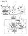
- FIG. 2 is a diagram of the structure of the portable phone 1.
- This portable phone 1 includes a communication unit 2, a call transmitting and receiving unit 3, an operating unit 4, a control unit 5, the display unit 6, the touch panel 7, a power supply unit 8, a driver unit 71 of the touch panel 7, and others.
- the driver unit 71 of the touch panel 7 depicted in the drawing is of a separate type externally mounted on the touch panel 7, this is not meant to be restrictive.
- the driver unit 71 may be of an integrated type incorporated inside the touch panel 7.
- the communication unit 2 wirelessly transmits and receives analog or digital data to and from the nearest base station (omitted in the drawing) via an antenna 2a, and this data contains information about incoming calls and outgoing calls and information about voice calls and, if necessary, contents information when, for example, contents on the Internet are used (downloaded), and information about transmission and reception of electronic mails.
- the call transmitting and receiving unit 3 includes a microphone and a loudspeaker not depicted in the drawing and, under the control from the control unit 5, this call transmitting and receiving unit 3 converts a voice signal from the microphone into digital data for output to the control unit 105 and converts a digital voice signal outputted from the control unit 5 into an analog signal for output from the loudspeaker.
- the operating unit 4 includes various operation buttons (such as a power supply switch, ten keys, and a function key: refer to the operation button group 104 of FIG. 1 ) for necessary user input to the control unit 5, and the power supply unit 8 includes a battery (a primary battery or a chargeable secondary battery) for supplying power necessary for this portable phone 1.
- various operation buttons such as a power supply switch, ten keys, and a function key: refer to the operation button group 104 of FIG. 1
- the power supply unit 8 includes a battery (a primary battery or a chargeable secondary battery) for supplying power necessary for this portable phone 1.
- the display unit 6 is a flat display device such as a liquid-crystal display.
- the touch panel 7 of the projected capacitive type is affixed to a display surface of this display unit 6, the touch panel 7 of the projected capacitive type is affixed. While the display unit 6 and the touch panel 7 are drawn in the drawing so as to be slightly shifted in a surface direction, this is for convenience of description. In practice, the touch panel 7 of a planar size approximately equal to that of the display surface is placed so as to cover the entire display surface of the display unit 6. Also, the display unit 6 and the touch panel 7 are not necessarily separate components. For example, an integrated type is possible in which the touch panel 7 is incorporated on an upper layer side of a display layer (such as a liquid-crystal layer) of the display unit 6. The detailed structure of the touch panel 7 and its operation will be described further below.
- the control unit 5 is a control element of a program control type including a microcomputer or simply a computer (hereinafter, a CPU) 5a, a rewritable non-volatile semiconductor memory (hereinafter, a PROM) 5b, a high-speed semiconductor memory (hereinafter, a RAM) 5c, and peripheral circuits not depicted in the drawing.
- a CPU microcomputer or simply a computer
- PROM rewritable non-volatile semiconductor memory
- RAM high-speed semiconductor memory
- the control programs include a basic program called a so-called operating system (OS) supporting a graphical user interface and also a necessary driver program, in detail, a dedicated program necessary for the operation of specific hardware, for example, a driver program for the touch panel 7 and further include, together with these basic program and the driver program, a dedicated application program (application program) for achieving a specific function (in the example depicted in the drawing, a portable phone function).
- OS operating system
- application program application program for achieving a specific function (in the example depicted in the drawing, a portable phone function).
- the driver unit 71 of the touch panel 7 includes an analog circuit unit 72, a reference signal generating unit (OSC) 73 that generates an operation reference signal for the driver unit 71, and a microcomputer or simply a computer (CPU) 75 that controls the operation of each of units (such as a signal source 19, a scan driving unit 18, an X electrode selecting unit 16, a Y electrode selecting unit 17, a threshold switching unit 21, and a response determining unit 20) mounted on the analog circuit unit 72 while executing a predetermined control program (firmware) stored in advance in a memory unit 74 and exchanges data with the control unit 5 of the portable phone 1 via an input and output unit 76.
- units such as a signal source 19, a scan driving unit 18, an X electrode selecting unit 16, a Y electrode selecting unit 17, a threshold switching unit 21, and a response determining unit 20
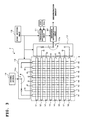
- FIG. 3 is a conceptual diagram of the structure of the touch panel 7.
- the touch panel 7 includes a touch unit 9 having a planar size (lengthwise and breadthwise dimensions) approximately equal to that of the display surface of the display unit 6.
- the touch unit 9 has a structure of a so-called mutual capacitance type that includes a plurality of electrodes in lengthwise and breadthwise directions uniformly arranged with fine spacing.
- each electrode is a long electrode having a constant width in this drawing, this is not meant to be restrictive.
- each electrode may be an electrode having a shape with squares, diamonds, or other shapes connected one after another.
- the lengthwise direction of the touch unit 9 (a vertical direction in the drawing) is set as a Y-axis direction
- the breadthwise direction (a horizontal direction in the drawing) is set as an X-axis direction
- the respective electrodes arranged in the lengthwise direction are provided with reference characters Y1 to Y8
- the respective electrodes arranged in the breadthwise direction are provided with reference characters X1 to X8.
- the number of electrodes (eight X and eight Y, respectively) depicted in the drawings is merely by way of example for description. Depending on the planar size of the touch unit 9, the number amounts to several hundred to several thousands in practice. Also, the touch unit 9 including the electrodes Y1 to Y8 and X1 to X8 is made of a translucent material, allowing any display information displayed on the display surface of the display unit 6 positioned on a rear surface side of the touch unit 9 to be viewable through this touch unit 9.
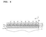
- FIG. 4 is a sectional view of the touch unit 9.
- the touch unit 9 includes a base transparent plate 10 such as a glass or a transparent film placed in contact with the display surface of the display unit 6, an X electrode layer 11 and a Y electrode layer 12 sequentially placed and laminated on the base transparent plate 10, and a protective transparent plate 13 such as a glass (preferably a toughened glass) or acrylic placed on an upper surface of the Y electrode layer 12.
- a protective film for preventing scattering of glass fragments is desirably affixed to the glass surface.
- the X electrode layer 11 has many electrodes X1 to X8 formed on a transparent dielectric film (for example, PET) 14 with fine spacing.
- the Y electrode layer 12 has many electrodes Y1 to Y8 formed on a transparent dielectric film 15 with fine spacing.
- the electrodes X1 to X8 and Y1 to Y8 are formed by vapor-deposition, coating, or printing of a transparent conductive material, for example, ITO (Indium Tin Oxide).
- Two electrode layers have the same structure, except for an electrode arranging direction. However, they are different in that, as depicted in the drawing, the X electrode layer 11 and the Y electrode layer 12 are sequentially placed and laminated on the base transparent plate 10 and, in the example depicted in the drawing, the Y electrode layer 12 is positioned on the X electrode 11, and therefore the Y electrode layer 12 is an upper layer, that is, at a position near the surface of the touch unit 9 (a touch surface 9a). Note that this vertical relation may be reversed. That is, the X electrode layer 11 may be at an upper layer position.
- description continues with the vertical relation assumed as depicted in the drawing (the Y electrode layer 12 is above the X electrode layer 11).
- the X electrode selecting unit 16 is connected to one end side of the electrodes X1 to X8 and, similarly, the Y electrode selecting unit 17 is connected to one end side of the electrodes Y1 to Y8.
- These X electrode selecting unit 16 and Y electrode selecting unit 17 select one of the electrodes X1 to X8 and one of the electrodes Y1 to Y8, respectively in a line-sequential manner in response to a scanning signal from the scan driving unit 18.
- the line-sequential method may be performed for each row (Y) or each column (X). For example, each column (X) may be selected for each row (Y), or each row (Y) may be selected for each column (X).
- the latter method is assumed to be adopted.
- the X electrode selecting unit 16 and the Y electrode selecting unit 17 sequentially select the Y electrodes from the first row to the eighth row (Y1 to Y8) during the selection, then, while selecting the X electrode on the second column (X2), they sequentially select the Y electrodes from the first row to the eighth row (Y1 to Y8) during the selection, ..., and, finally, while selecting the X electrode on the eighth row (X8), they sequentially select the Y electrodes from the first row to the eighth row (Y1 to Y8) during the selection.
- the electrodes X1 to X8 and the electrodes Y1 to Y8 are selected in a line-sequential manner. Note that while description has been made with a sequential selecting scheme, this is not meant to be restrictive. For example, a thinning-out selecting scheme may be adopted, such as skipping every other electrode or skipping every plural electrodes.
- Eight-contact rotary switches 16a and 17a drawn in frames of the X electrode selecting unit 16 and the Y electrode selecting unit 17 are depicted so as to schematically depict a selecting operation of the X electrode selecting unit 16 and the Y electrode selecting unit 17, respectively.
- the X electrode selecting unit 16 supplies a drive signal (an alternating current signal with a predetermined frequency and at a predetermined signal level) from the signal source 19 to a selected electrode (any one of X1 to X1) via a contact of the rotary switch 16a.
- the Y electrode selecting unit 17 takes out a drive signal (one supplied from the signal source 19) passing through a capacitance between a selected electrode (any one of Y1 to Y1) and the X electrode selected by the X electrode selecting unit 16 at that moment via a contact of the rotary switch 17a, and then outputs the drive signal to the response determining unit 20.
- the response determining unit 20 removes noise (such as a signal other than the drive signal generated at the signal source 19) from the drive signal taken out via the Y electrode selecting unit 17 for direct current electrification of the signal after removal of noise, and then compares this direct current signal with a predetermined determination threshold to determine whether a touch operation or a hover operation has been performed on the touch unit 9, and outputs the determination result to the control unit 5 as a predetermined event signal (a touch event or a hover event).
- noise such as a signal other than the drive signal generated at the signal source 19
- the threshold switching unit 21 In response to the scanning signal from the scan driving unit 18, the threshold switching unit 21 appropriately switches between these thresholds SLH and SLL for output to the response determining unit 20.
- the response determining unit 20 uses the threshold outputted from the threshold switching unit 21 to make a response determination as to whether the operation is a touch or hover operation.
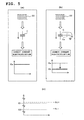
- FIG. 5 shows diagrams for describing the principle of response determination as to whether the operation is a touch or hover operation.
- a drive signal 22 generated at the signal source 19 is applied to one end of a capacitor C.
- the capacitor C represents a capacitance occurring between paired XY electrodes selected by the X electrode selecting unit 16 and the Y electrode selecting unit 17, and the drive signal 22 is an alternating current signal.
- a capacitance Ca of the human body acts on the capacitor C, as depicted in (b), thereby causing leakage of the drive signal 22 via this capacitance Ca.
- the human body is regarded as a grounded body with the capacitance Ca. Due to this leakage, the drive signal 22 passing through the capacitor C is decreased and, in the end, a direct current voltage Eb of the drive signal 2 passing through the capacitor C is smaller than the direct current voltage Ea of (a) described above. Therefore, to differentiate between the presence and absence of a touch operation, it is sufficient to use appropriate thresholds capable of determining the direct current voltages Ea and Eb.
- a hover operation is a non-touch operation but in the state in which part of the human body such as a fingertip is near the touch surface 9a of the touch unit 9, the capacitance of the human body acts on the capacitor C also in this state.
- the human capacitance in this state is smaller than the capacitance Ca at the time of touch operation, a threshold for hover operation determination is required to be allocated to a higher sensitivity side than the threshold for touch operation determination described above.
- the thresholds of two types, SLH and SLL, in the present embodiment are decided in consideration of the above, and the highly-sensitive detection threshold SLH is for hover operation determination and the lowly-sensitive detection threshold SLL is for touch operation determination. Note that these words “highly-sensitive” and “lowly-sensitive” do not have particular meanings.
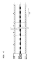
- FIG. 6 is a timing diagram of an electrode scanning order and an application order of two thresholds.
- the uppermost row represents a scanning order of the electrodes Y1 to Y8 and X1 to X8.
- This drawing depicts an example of line-sequential scanning in which each row (Y) is scanned for each column (X). That is, while the X electrode on the first column (X1) is selected, the Y electrodes from the first row to the eighth row (Y1 to Y8) are sequentially selected during the selection, then, while the X electrode on the second column (X2) is selected, the Y electrodes from the first row to the eighth row (Y1 to Y8) are sequentially selected during the selection, ... (omitted) ...
- the intermediate row represents the first pattern, and the lowermost row represents the second pattern.
- the highly-sensitive detection threshold SLH and the lowly-sensitive detection threshold SLL are alternately applied for each scanning of the electrodes Y1 to Y8.
- the highly-sensitive detection threshold SLH is applied when odd-numbered Y electrodes (Y1, Y3, Y5, Y7) are scanned and the lowly-sensitive detection threshold SLL is applied when even-numbered Y electrodes (Y2, Y4, Y6, Y8) are scanned, but this may be reversed (the odd-numbered Y electrodes ⁇ the lowly-sensitive detection threshold SLL, the even-numbered Y electrodes ⁇ the highly-sensitive detection threshold SLH).
- the lowly-sensitive detection threshold SLL is applied to all of the Y electrodes (Y1 to Y8).
- FIG. 7 is a diagram of a control operation flow of the touch panel 7. Main parts of this operation flow are achieved in software by firmware executed at the CPU 75 of the driver unit 71 of the touch panel 7 and the control program executed at the CPU 5a of the control unit 5 (such as part of the basic program and the driver program of the touch panel 7).
- electrodes near the panel surface (the touch surface 9a of the touch unit 9) (Y electrodes on an upper layer side in the example of structure of FIG. 4 ) are first grouped into highly-sensitive hover electrodes and lowly-sensitive touch electrodes (Step S1). This grouping is desirably performed so that the hover electrodes and the touch electrodes are distributed as uniformly as possible.
- the first pattern described above depicts a practical example of this grouping.
- adjacent Y electrodes are allocated as a hover electrode and a touch electrode so that "the highly-sensitive detection threshold SLH and the lowly-sensitive detection threshold SLL are alternately applied for each scanning of the electrodes Y1 to Y8"
- this first pattern is the most preferable example in which the hover electrodes and the touch electrodes are uniformly distributed.
- FIG. 8 is a diagram of pattern classification into hover electrodes and touch electrodes.
- the hover electrode response refers to the state in which a detection signal with a magnitude corresponding to the highly-sensitive detection threshold SLH (a direct current voltage after the drive signal taken out via the capacitance of the XY electrodes during the selection is direct current electrification) has been detected at the response determining unit 20.
- a hover electrode response is not determined, the determination process is looped. If a hover electrode response is determined, it is determined that part of the human body such as a fingertip is near the touch surface 9a of the touch unit 9, and subsequently a determination as to "touch electrode response" is made (Step S3).
- the touch electrode response refers to the state in which a detection signal with a magnitude corresponding to the lowly-sensitive detection threshold SLL (a direct current voltage after the drive signal taken out via the capacitance of the XY electrodes during the selection is direct current electrification) has been detected at the response determining unit 20.
- SLL a direct current voltage after the drive signal taken out via the capacitance of the XY electrodes during the selection is direct current electrification
- Step S4 if a touch electrode response is not determined, it is determined that a hover operation has been performed, and coordinates of XY electrodes at the time of detecting the detection signal with the magnitude corresponding to the highly-sensitive detection threshold SLH are detected as hover coordinates (Step S4), and also a predetermined event signal including this coordinate information (hereinafter, a hover event) is generated (Step S5). The procedure then returns to Step S2 again.
- Step S3 when a touch electrode response is determined at Step S3, it is determined that a touch operation was performed immediately after the hover operation.
- the lowly-sensitive detection threshold SLL is applied to all of the Y electrodes to set touch electrodes (Step S6), and then coordinates of XY electrodes at the time of detecting the detection signal with the magnitude corresponding to the lowly-sensitive detection threshold SLL are detected as touch coordinates (Step S7), and also a predetermined event signal including this coordinate information (hereinafter, a touch event) is generated (Step S8). Then a determination as to a touch electrode response is again made (Step S9). If a touch electrode response is present, the procedure repeats Step S7 to Step S9. On the other hand, if a touch electrode response is absent, the procedure returns to Step S1 again.
- FIG. 9 is a diagram of threshold application when a touch operation is determined.
- the lowly-sensitive detection threshold SLL is applied to all of the Y electrodes (Y1 to Y8).
- This measure is performed exclusively in order to enhance the resolution of detecting touch coordinates. That is, this measure is performed in order to enhance the resolution of detecting touch coordinates (also referred to as detection accuracy) by using all of the Y electrodes as touch detection electrodes to a degree of the space among Y1 to Y8, and is not a requisite matter for improving detection responsiveness to a touch operation or detecting and differentiating between a hover operation and a touch operation.
- the hover event and the touch even are used as appropriate as an impetus for performing any process in the basic program and the application program to be executed at the CPU 5a of the control unit 5.
- the position of a cursor (a sign such as an under line or an arrow for indicating an input position displayed on a screen, and is also referred to as a caret or an insertion pointer) may be controlled.
- a determining process corresponding to a return key operation on a keyboard or a click operation on a mouse may be performed.
- the touch panel 7 of the present embodiment performs the operations described above, main points of these operations are described.
- the electrodes near the panel surface (Y1 to Y8) are grouped into hover electrodes with a high degree of sensitivity and touch electrodes with a low degree of sensitivity and, in the grouped state, determinations as to a hover operation and a touch operation are separately made. That is, when the determination result at Step S2 is YES and the determination result at Step S3 is NO, it is determined that "a hover operation is present". When the determination result at Step S2 is YES and the determination result at Step S3 is YES, it is determined that "a touch operation is present".
- a first effect can be obtained in which a hover operation and a touch operation can be differentiated and detected, and a second effect can also be obtained in which a determination as to a touch operation immediately after a hover operation can be quickly made, thereby not inviting deterioration in responsiveness of a determination as to a touch operation.
- the adjusting function for differentiating between touch detection and hover detection can be provided so as to be spatially divided for touch detection and hover detection, with each detection mechanism appropriately place, touch detection and hover detection can be concurrently made. Therefore, detection of not only a state in contact with the touch panel surface but also a state near the touch panel surface can be made with sufficient accuracy, and an improvement in detection accuracy can be achieved.
- a sensitivity change between a hover electrode and a touch electrode is performed by switching between thresholds (SLH, SLL), this is not meant to be restrictive.
- the sensitivity of the hover electrode can be set relatively higher than the sensitivity of the touch electrode and, for example, the following may be applied.
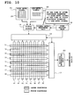
- FIG. 10 is a diagram of another example of a sensitivity change.
- a signal level switching unit 23 is provided in place of the threshold switching unit 21 for switching between the two thresholds (SLH, SLL).
- This signal level switching unit 23 is to switch the drive signal generated at the signal source 19 to one of a high-level signal 26 from a high-level signal generation source 24 and a low-level signal 27 from a low-level signal generation source 25, and switching timing is similar to that between two thresholds (SLH, SLL) described above.
- timing is such that the high-level signal 26 is applied when the odd-numbered Y electrodes (Y1, Y3, Y5, Y7) are scanned as hover electrodes, and the low-level signal 27 is applied when the even-numbered Y electrodes (Y2, Y4, Y6, Y8) are scanned as touch electrodes.
- the odd-numbered Y electrodes are hover electrodes and the even-numbered Y electrodes are touch electrodes, and these hover electrodes (the odd-numbered Y electrodes) are driven with the high-level signal 26 and these touch electrodes (the even-numbered Y electrodes) are driven with the low-level signal 27. Therefore, as with the threshold switching scheme described above, the sensitivity of the hover electrodes can be made relatively higher than the sensitivity of the touch electrodes.
- the first effect can be obtained in which a hover operation and a touch operation can be differentiated and detected and, furthermore, the second effect can also be obtained in which a determination as to a touch operation immediately after a hover operation can be quickly made, thereby not inviting deterioration in responsiveness of a determination as to a touch operation.
- the present invention is not restricted to this mode, and may be as follows.
- FIG. 11 is a diagram of another example of allocation of hover electrodes and touch electrodes. This drawing corresponds to the sectional view of the touch unit 9 depicted in FIG. 4 described above. A difference from FIG. 4 is that part of the Y electrodes (Y1, Y3, Y5, Y7) formed on the Y electrode layer 12 are moved onto the protective transparent plate 13 and the moved Y electrodes (Y1, Y3, Y5, Y7) are protected with a film 28 (for example, a glass-scattering-preventive film).
- a film 28 for example, a glass-scattering-preventive film.
- part of the Y electrodes (Y1, Y3, Y5, Y7) are brought closer to the touch surface (a surface of the film 28) than the other Y electrodes (Y2, Y4, Y6, Y8). Therefore, without requiring switching a threshold or a drive signal, part of the Y electrodes (Y1, Y3, Y5, Y7) can be used as hover electrodes with a high degree of sensitivity and the other electrodes (Y2, Y4, Y6, Y8) can be used as touch electrodes with a low degree of sensitivity.
- FIG. 12 shows diagrams of other structures of the touch panel.
- an X electrode layer 30 having X electrodes (X1 to X8) equidistantly arranged and formed on a first dielectric layer 29 made of PET or the like and a Y electrode layer 32 having Y electrodes (Y1 to Y8) equidistantly arranged and formed on a second dielectric layer 31 similarly made of PET or the like are laminated with an adhesive 33.
- the touch panel 7 with a touch unit 36 having a structure in which the Y electrode layer 32 and a transparent cover body 34 such as a protective toughened glass are laminated with an adhesive 35 may be used.
- a touch panel may have a structure in which the X electrodes and the Y electrodes are formed on the same layer.
- (b) is a plan view of this type, and X electrodes 37 and the Y electrodes 38 depicted as being partially representative include electrode units 37a and 38a alternately arranged on the same layer and connecting units 37b and 38b each connecting electrodes aligned in the same direction (an X direction, a Y direction), in which one connecting unit goes across the other connecting unit (in the drawing, the connecting unit 37b goes across the connecting unit 38b).
- (c) is a sectional view of this type, with a structure in which the X electrodes 37 and the Y electrodes 38 are formed and arranged on a transparent substrate 39 such as a glass and, on these electrodes, a transparent cover body 41 such as a protective toughened glass is laminated by using an adhesive 40.
- a main point of the present embodiment is that part of ones of the X electrodes and the Y electrodes are set as hover electrodes for detecting a hover operation and the remaining are set as touch electrodes for detecting a touch operation. It is sufficient to set hover electrodes for detecting a hover operation at "at least" part of either of the X electrodes and the Y electrodes. While part of the "Y electrodes", which are ones of the X electrodes and the Y electrodes, are set as hover electrode for detecting a hover operation in the embodiment described above, this merely describes one of enabled modes. Part of the "X electrodes" may be set as hover electrodes for detecting a hover operation, or the following may be possible.
- FIG. 13 shows diagrams of other modes of allocation of hover electrodes.
- (a) depicts an example in which part of the X electrodes (in this drawing, X1, X3, X5, X7) and part of the Y electrodes (in this drawing, Y1, Y3, Y5, Y7) are allocated as hover electrodes for detecting a hover operation.
- (b) depicts an example in which all of the X electrodes (X1 to X8) and part of the Y electrodes (in this drawing, Y1, Y3, Y5, Y7) are allocated as hover electrodes for detecting a hover operation.
- the degree of density of hover electrodes is low in (a) and therefore there is a disadvantage of low detection resolution on one hand.
- a low degree of density means a small number of electrodes to be driven as hover electrodes, and thus "the number of electrodes to be driven ⁇ small ⁇ drive power ⁇ small" is established.
- an advantage of power saving can be suggested.
- This advantage (power saving) also applies in the embodiment described above, because part of either of the X electrodes and the Y electrodes are set as hover electrodes in the embodiment and the degree of density of hover electrodes are similar to or lower than that depicted in (a).
- An input device including:
- the input device wherein the setting means resets the hover electrodes as touch electrodes for touch operation detection when a touch operation is detected by the touch electrodes.
- the setting means since all of either of the X electrodes and the Y electrodes are set as touch electrodes, resolution of detecting a touch operation can be enhanced.
- the input device including:
- the input device wherein the electric characteristic of the pair is a capacitance
- the detecting means detects a change of the capacitance by comparing a signal value indicating the change of the capacitance and a threshold
- the switching means switches the detection sensitivity of the detecting means by changing the threshold of the detecting means.
- a predetermined threshold a highly-sensitive detection threshold
- another predetermined threshold a lowly-sensitive detection threshold
- the detecting means detects a change of the capacitance by comparing a magnitude of a drive signal applied to one end of the capacitance and appearing at another end of the capacitance or a signal value indicating the magnitude and a threshold, and the switching means switches the detection sensitivity of the detecting means by changing the magnitude of the drive signal applied to the one end of the capacitance or the signal value indicating the magnitude.
- Supplementary Note 6 only by setting a drive signal (a high-level signal) with a magnitude suitable for detecting a hover operation and a drive signal (a low-level signal) with a magnitude suitable for detecting a touch operation, an effect of Supplementary Note 1 can be obtained, that is, detection of not only a state in contact with the touch panel surface but also a state near the touch panel surface can be made with sufficient accuracy and an improvement in detection accuracy can be achieved.
- An input control method including:
- An electronic device including the input device according to Supplementary Note 1 includes the input device according to Supplementary Note 1.
- a touch panel of the capacitive type for example, a personal computer, a portable phone, a portable information terminal, a portable game machine, an electronic dictionary, an electronic book display terminal, as with Supplementary Note 1, detection of not only a state in contact with the touch panel surface but also a state near the touch panel surface can be made with sufficient accuracy and an improvement in detection accuracy can be achieved.
Landscapes
- Engineering & Computer Science (AREA)
- General Engineering & Computer Science (AREA)
- Theoretical Computer Science (AREA)
- Human Computer Interaction (AREA)
- Physics & Mathematics (AREA)
- General Physics & Mathematics (AREA)
- Position Input By Displaying (AREA)
Applications Claiming Priority (2)
| Application Number | Priority Date | Filing Date | Title |
|---|---|---|---|
| JP2010293161 | 2010-12-28 | ||
| PCT/JP2011/006942 WO2012090405A1 (ja) | 2010-12-28 | 2011-12-13 | 入力装置、入力制御方法、プログラム及び電子機器 |
Publications (2)
| Publication Number | Publication Date |
|---|---|
| EP2660685A1 true EP2660685A1 (de) | 2013-11-06 |
| EP2660685A4 EP2660685A4 (de) | 2017-03-22 |
Family
ID=46382547
Family Applications (1)
| Application Number | Title | Priority Date | Filing Date |
|---|---|---|---|
| EP11853280.3A Withdrawn EP2660685A4 (de) | 2010-12-28 | 2011-12-13 | Eingabevorrichtung, eingabesteuerungsverfahren, programm und elektronische vorrichtung |
Country Status (5)
| Country | Link |
|---|---|
| US (1) | US9383868B2 (de) |
| EP (1) | EP2660685A4 (de) |
| JP (1) | JP6024903B2 (de) |
| CN (1) | CN103282863B (de) |
| WO (1) | WO2012090405A1 (de) |
Cited By (2)
| Publication number | Priority date | Publication date | Assignee | Title |
|---|---|---|---|---|
| WO2015134347A1 (en) * | 2014-03-03 | 2015-09-11 | Microchip Technology Incorporated | System and method for gesture control |
| EP3614241A4 (de) * | 2017-04-20 | 2021-01-06 | Alps Alpine Co., Ltd. | Elektronische vorrichtung vom berührungssensortyp und sensorsteuerverfahren |
Families Citing this family (37)
| Publication number | Priority date | Publication date | Assignee | Title |
|---|---|---|---|---|
| JP4888853B2 (ja) | 2009-11-12 | 2012-02-29 | 学校法人慶應義塾 | 液晶表示装置の視認性改善方法、及びそれを用いた液晶表示装置 |
| CN110187549B (zh) | 2010-06-22 | 2022-07-15 | 东洋纺株式会社 | 液晶显示装置、偏振板及偏振片保护膜 |
| JP6004563B2 (ja) * | 2012-04-19 | 2016-10-12 | 株式会社ジャパンディスプレイ | 表示装置 |
| WO2014024366A1 (ja) * | 2012-08-09 | 2014-02-13 | パナソニック株式会社 | 携帯電子機器 |
| JP5565598B1 (ja) * | 2013-02-01 | 2014-08-06 | パナソニック インテレクチュアル プロパティ コーポレーション オブ アメリカ | 電子機器、入力処理方法、およびプログラム |
| JP6012532B2 (ja) * | 2013-04-03 | 2016-10-25 | 三菱電機株式会社 | タッチスクリーン、及び、それを備えるタッチパネル |
| CN103279248B (zh) * | 2013-06-06 | 2017-03-01 | 敦泰科技有限公司 | 集成触控有机发光二极管显示装置 |
| US20140375590A1 (en) * | 2013-06-19 | 2014-12-25 | Ronald Steven Cok | Multi-resolution micro-wire touch-sensing method |
| JP2015011679A (ja) * | 2013-07-02 | 2015-01-19 | シャープ株式会社 | 操作入力装置及び入力操作処理方法 |
| JP6115719B2 (ja) * | 2013-08-12 | 2017-04-19 | アルパイン株式会社 | 電子装置、電子装置のディスプレイの移動方法および移動プログラム |
| JP2015045909A (ja) * | 2013-08-27 | 2015-03-12 | 株式会社東海理化電機製作所 | 操作入力装置 |
| JP6187043B2 (ja) * | 2013-08-29 | 2017-08-30 | 富士通株式会社 | タッチ検出装置 |
| KR102140791B1 (ko) * | 2013-10-11 | 2020-08-03 | 삼성전자주식회사 | 터치 컨트롤러, 터치 컨트롤러를 포함하는 디스플레이 장치 및 전자 장치, 및 터치 센싱 방법 |
| KR101466506B1 (ko) * | 2013-10-17 | 2014-11-28 | 주식회사 동부하이텍 | 터치 패널 및 그 구동방법 |
| US9606664B2 (en) * | 2013-11-13 | 2017-03-28 | Dell Products, Lp | Dynamic hover sensitivity and gesture adaptation in a dual display system |
| KR102192521B1 (ko) * | 2013-12-31 | 2020-12-17 | 엘지디스플레이 주식회사 | 터치 스크린 장치, 이를 이용한 터치 스크린 표시장치 및 그 구동 방법 |
| CN106104438A (zh) * | 2014-01-16 | 2016-11-09 | 触觉实验室股份有限公司 | 在触摸敏感设备中以减小的灵敏度进行操作的设备和方法 |
| KR102245943B1 (ko) * | 2014-06-23 | 2021-04-29 | 엘지디스플레이 주식회사 | 터치 패널 및 이의 구동 장치 |
| JP2016038840A (ja) * | 2014-08-11 | 2016-03-22 | シャープ株式会社 | 通信装置、通信装置の制御方法および通信装置の制御プログラム |
| JP6472196B2 (ja) * | 2014-09-17 | 2019-02-20 | 株式会社ワコム | センサ信号処理回路及びセンサ信号処理方法 |
| KR20160056759A (ko) * | 2014-11-12 | 2016-05-20 | 크루셜텍 (주) | 이미지 스캔이 가능한 플렉서블 디스플레이 장치 및 이의 구동 방법 |
| KR102352181B1 (ko) * | 2015-04-15 | 2022-01-17 | 삼성디스플레이 주식회사 | 터치 패널 및 이를 이용한 터치 패널의 구동 방법 |
| KR102353484B1 (ko) * | 2015-05-27 | 2022-01-20 | 엘지전자 주식회사 | 반도체 발광 소자를 이용한 디스플레이 장치 |
| KR20170000187A (ko) * | 2015-06-23 | 2017-01-02 | 삼성전자주식회사 | 디스플레이 장치 |
| CN106371685A (zh) * | 2016-09-30 | 2017-02-01 | 苏州欧菲光科技有限公司 | 电子设备及其悬浮电容式触摸屏 |
| JP6901949B2 (ja) * | 2017-09-29 | 2021-07-14 | 株式会社ジャパンディスプレイ | 検出装置及び表示装置 |
| US10437365B2 (en) | 2017-10-11 | 2019-10-08 | Pixart Imaging Inc. | Driver integrated circuit of touch panel and associated driving method |
| CN108362427B (zh) * | 2018-01-31 | 2024-08-16 | 北京他山科技有限公司 | 一种具有多功能层的接触传感器、电子皮肤和智能机器人 |
| CN110727366B (zh) * | 2018-07-17 | 2024-04-26 | 安徽精卓光显技术有限责任公司 | 触控结构、触控结构的制作方法、触控显示屏及电子设备 |
| FR3086079B1 (fr) * | 2018-09-17 | 2021-04-23 | Zodiac Aero Electric | Dispositif tactile multitouche a detection capacitive |
| KR102650376B1 (ko) | 2018-11-02 | 2024-03-25 | 삼성전자주식회사 | 터치 인식을 위한 센서 및 호버링 인식을 위한 센서를 포함하는 전자 장치 및 그 동작 방법 |
| EP3726349A1 (de) * | 2019-03-04 | 2020-10-21 | Shenzhen Goodix Technology Co., Ltd. | Schwebezustandsbestimmungs- und schwebezustandskompensierungsverfahren und -vorrichtungen für berührungsbildschirm |
| US11366558B2 (en) | 2019-07-26 | 2022-06-21 | Apple Inc. | Metal mesh touch electrodes with visibility mitigations |
| JP7194666B2 (ja) * | 2019-11-19 | 2022-12-22 | 株式会社ヴァレオジャパン | 表示装置 |
| KR102566581B1 (ko) * | 2019-11-19 | 2023-08-11 | 알프스 알파인 가부시키가이샤 | 정전 용량식 센서, 정전 용량 검출 방법, 및 정전 용량 검출 프로그램 |
| US11762515B1 (en) * | 2022-05-27 | 2023-09-19 | Samsung Electronics Co., Ltd. | Touch and hover sensing on single-layer segmented sheets |
| US12481394B1 (en) * | 2024-07-26 | 2025-11-25 | Dell Products L.P. | Three dimensional proximity detection for information handling system |
Family Cites Families (12)
| Publication number | Priority date | Publication date | Assignee | Title |
|---|---|---|---|---|
| JP2003330618A (ja) | 2002-05-16 | 2003-11-21 | Sony Corp | 入力方法及び入力装置 |
| JP5324440B2 (ja) | 2006-07-12 | 2013-10-23 | エヌ−トリグ リミテッド | デジタイザのためのホバリングおよびタッチ検出 |
| US8284165B2 (en) | 2006-10-13 | 2012-10-09 | Sony Corporation | Information display apparatus with proximity detection performance and information display method using the same |
| JP4766340B2 (ja) * | 2006-10-13 | 2011-09-07 | ソニー株式会社 | 近接検知型情報表示装置およびこれを使用した情報表示方法 |
| JP2008134836A (ja) * | 2006-11-28 | 2008-06-12 | Wacom Co Ltd | タッチパネル装置 |
| US20080297487A1 (en) | 2007-01-03 | 2008-12-04 | Apple Inc. | Display integrated photodiode matrix |
| US7679376B2 (en) * | 2007-01-19 | 2010-03-16 | Korea Institute Of Science And Technology | Capacitive sensor for sensing tactile and proximity, and a sensing system using the same |
| US20090128515A1 (en) * | 2007-11-02 | 2009-05-21 | Bytheway Jared G | Proximity sensing by increasing gain in touchpad circuitry and increasing distance between sensor electrodes and a sense electrode |
| JPWO2009107415A1 (ja) | 2008-02-27 | 2011-06-30 | セイコーインスツル株式会社 | 近接検出装置と近接検出方法 |
| US9323398B2 (en) * | 2009-07-10 | 2016-04-26 | Apple Inc. | Touch and hover sensing |
| JP5229273B2 (ja) * | 2010-05-28 | 2013-07-03 | 株式会社Jvcケンウッド | タッチパネルを有する電子機器、及び動作制御方法 |
| CN102576276B (zh) * | 2010-08-23 | 2017-05-10 | 谱瑞科技股份有限公司 | 电容扫描邻近侦测 |
-
2011
- 2011-12-13 WO PCT/JP2011/006942 patent/WO2012090405A1/ja not_active Ceased
- 2011-12-13 US US13/976,760 patent/US9383868B2/en not_active Expired - Fee Related
- 2011-12-13 CN CN201180063322.5A patent/CN103282863B/zh not_active Expired - Fee Related
- 2011-12-13 JP JP2012550695A patent/JP6024903B2/ja not_active Expired - Fee Related
- 2011-12-13 EP EP11853280.3A patent/EP2660685A4/de not_active Withdrawn
Non-Patent Citations (1)
| Title |
|---|
| See references of WO2012090405A1 * |
Cited By (6)
| Publication number | Priority date | Publication date | Assignee | Title |
|---|---|---|---|---|
| WO2015134347A1 (en) * | 2014-03-03 | 2015-09-11 | Microchip Technology Incorporated | System and method for gesture control |
| CN105980974A (zh) * | 2014-03-03 | 2016-09-28 | 密克罗奇普技术公司 | 用于手势控制的系统及方法 |
| JP2017507416A (ja) * | 2014-03-03 | 2017-03-16 | マイクロチップ テクノロジー インコーポレイテッドMicrochip Technology Incorporated | ジェスチャ制御のためのシステムおよび方法 |
| US9921739B2 (en) | 2014-03-03 | 2018-03-20 | Microchip Technology Incorporated | System and method for gesture control |
| US20180188922A1 (en) * | 2014-03-03 | 2018-07-05 | Microchip Technology Incorporated | System and Method for Gesture Control |
| EP3614241A4 (de) * | 2017-04-20 | 2021-01-06 | Alps Alpine Co., Ltd. | Elektronische vorrichtung vom berührungssensortyp und sensorsteuerverfahren |
Also Published As
| Publication number | Publication date |
|---|---|
| US9383868B2 (en) | 2016-07-05 |
| CN103282863A (zh) | 2013-09-04 |
| JP6024903B2 (ja) | 2016-11-16 |
| US20130278560A1 (en) | 2013-10-24 |
| EP2660685A4 (de) | 2017-03-22 |
| JPWO2012090405A1 (ja) | 2014-06-05 |
| WO2012090405A1 (ja) | 2012-07-05 |
| CN103282863B (zh) | 2016-10-05 |
Similar Documents
| Publication | Publication Date | Title |
|---|---|---|
| US9383868B2 (en) | Input device, input control method, program and electronic apparatus | |
| KR102446706B1 (ko) | 복합 휴먼 인터페이스가 구비된 전자기기 | |
| US8278571B2 (en) | Capacitive touchscreen or touchpad for finger and active stylus | |
| JP5818145B2 (ja) | 入力装置及び入力制御プログラム並びに入力制御方法 | |
| KR20170124068A (ko) | 복합 휴먼 인터페이스가 구비된 전자기기 | |
| CN112470108A (zh) | 用于触摸屏的机械键盘覆盖物 | |
| KR20110138743A (ko) | 측면 및 후면 터치센서가 구비된 모바일 장치 | |
| JP5759658B2 (ja) | 入力システムおよび電子機器の操作方法 | |
| US20220137716A1 (en) | Measuring Capacitance | |
| KR20190025472A (ko) | 복합 휴먼 인터페이스가 구비된 전자 기기 및 그 제어 방법 | |
| KR102015313B1 (ko) | 복합 휴먼 인터페이스가 구비된 전자 기기 및 그 제어 방법 | |
| KR102015309B1 (ko) | 복합 휴먼 인터페이스가 구비된 전자 기기 및 그 제어 방법 |
Legal Events
| Date | Code | Title | Description |
|---|---|---|---|
| PUAI | Public reference made under article 153(3) epc to a published international application that has entered the european phase |
Free format text: ORIGINAL CODE: 0009012 |
|
| 17P | Request for examination filed |
Effective date: 20130717 |
|
| AK | Designated contracting states |
Kind code of ref document: A1 Designated state(s): AL AT BE BG CH CY CZ DE DK EE ES FI FR GB GR HR HU IE IS IT LI LT LU LV MC MK MT NL NO PL PT RO RS SE SI SK SM TR |
|
| DAX | Request for extension of the european patent (deleted) | ||
| RAP1 | Party data changed (applicant data changed or rights of an application transferred) |
Owner name: NEC CORPORATION |
|
| RA4 | Supplementary search report drawn up and despatched (corrected) |
Effective date: 20170222 |
|
| RIC1 | Information provided on ipc code assigned before grant |
Ipc: G06F 3/044 20060101ALI20170216BHEP Ipc: G06F 3/041 20060101AFI20170216BHEP Ipc: G06F 3/0488 20130101ALI20170216BHEP |
|
| STAA | Information on the status of an ep patent application or granted ep patent |
Free format text: STATUS: THE APPLICATION HAS BEEN WITHDRAWN |
|
| 18W | Application withdrawn |
Effective date: 20180326 |