EP2660778A1 - Verfahren zur Festlegung eines Schwellwertes für die Bestimmung der kritischen Ausdehnung mindestens eines Bildmusters aufgenommen mittels Rasterkraftmikroskopie - Google Patents
Verfahren zur Festlegung eines Schwellwertes für die Bestimmung der kritischen Ausdehnung mindestens eines Bildmusters aufgenommen mittels Rasterkraftmikroskopie Download PDFInfo
- Publication number
- EP2660778A1 EP2660778A1 EP13166025.0A EP13166025A EP2660778A1 EP 2660778 A1 EP2660778 A1 EP 2660778A1 EP 13166025 A EP13166025 A EP 13166025A EP 2660778 A1 EP2660778 A1 EP 2660778A1
- Authority
- EP
- European Patent Office
- Prior art keywords
- threshold
- patterns
- empirical
- category
- image
- Prior art date
- Legal status (The legal status is an assumption and is not a legal conclusion. Google has not performed a legal analysis and makes no representation as to the accuracy of the status listed.)
- Withdrawn
Links
Images
Classifications
-
- G—PHYSICS
- G01—MEASURING; TESTING
- G01B—MEASURING LENGTH, THICKNESS OR SIMILAR LINEAR DIMENSIONS; MEASURING ANGLES; MEASURING AREAS; MEASURING IRREGULARITIES OF SURFACES OR CONTOURS
- G01B15/00—Measuring arrangements characterised by the use of electromagnetic waves or particle radiation, e.g. by the use of microwaves, X-rays, gamma rays or electrons
-
- G—PHYSICS
- G06—COMPUTING OR CALCULATING; COUNTING
- G06T—IMAGE DATA PROCESSING OR GENERATION, IN GENERAL
- G06T7/00—Image analysis
- G06T7/10—Segmentation; Edge detection
- G06T7/11—Region-based segmentation
-
- G—PHYSICS
- G06—COMPUTING OR CALCULATING; COUNTING
- G06T—IMAGE DATA PROCESSING OR GENERATION, IN GENERAL
- G06T7/00—Image analysis
- G06T7/10—Segmentation; Edge detection
- G06T7/174—Segmentation; Edge detection involving the use of two or more images
-
- H—ELECTRICITY
- H01—ELECTRIC ELEMENTS
- H01J—ELECTRIC DISCHARGE TUBES OR DISCHARGE LAMPS
- H01J37/00—Discharge tubes with provision for introducing objects or material to be exposed to the discharge, e.g. for the purpose of examination or processing thereof
- H01J37/26—Electron or ion microscopes; Electron or ion diffraction tubes
- H01J37/28—Electron or ion microscopes; Electron or ion diffraction tubes with scanning beams
Definitions
- the present invention relates to the field of metrology and relates to an optimized threshold determination method applicable to determine the critical dimension of at least one category of patterns imaged by scanning atomic force electron microscopy. This threshold thus determined can then be used in production to characterize patterns, in particular those used in microelectronic integrated circuits.
- the semiconductor industry defines and tracks the dimensions of products manufactured using the so-called Critical Dimension (CD) or Dimension Critique.
- CD Critical Dimension
- Dimension Critique The permanent decrease of the critical dimension of the circuits involves the corresponding adaptation of the measurement methods.
- the increase of the size of the wafers (or wafer in English) and the costs represented by each of them imply the control and the detection of the defects in production.
- CD Dimension Critique CD
- the vertical position of its measurement varies according to the reasons to be characterized.
- the CD of a transistor gate will be rather measured as low as possible while the CDs of a contact of grid or interconnection line will rather be measured as high as possible.
- a primary electron beam is emitted on the surface of the pattern to be analyzed which, in response, re-emits secondary electrons.
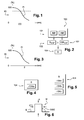
- These secondary electrons are analyzed by detectors that allow to reconstruct a graph as illustrated on the figure 1 representing a secondary electron intensity profile P1 comprising on the ordinate a percentage of secondary electrons collected and on the abscissa a dimension in nm representative of the CD.
- an empirically obtained secondary electron threshold of, for example, 80% is applicable to any type of pattern.
- the threshold of 80% is applied and the measured critical dimension is deduced therefrom regardless of the type of pattern analyzed.
- An empirical fixed threshold applied to any type of pattern is all the less satisfactory since there is no physical link between the percentage of secondary electrons collected and the actual height of the pattern at which the critical dimension is to be determined. In other words, if a measurement with 80% of secondary electrons is carried out, it does not mean that we measure a critical dimension at 80% of the height of the pattern.
- the object of the present invention is to provide a method for determining an applicable threshold for determining the critical dimension of at least one category of images imaged by scanning atomic force electron microscopy that can be used both in research and development. in production, to give a more accurate and realistic value of the critical dimension sought regardless of the level of manufacture to be characterized (eg level lithography or engraving level).
- the method according to the invention proposes, unlike the current CD metrology, to determine a threshold (applicable for at least one category of patterns) substantially close to the real threshold corresponding to the height at which the critical dimension is situated. we want to measure.
- threshold is meant a percentage of secondary electrons reemitted by a pattern subjected to a primary electron beam during a CD-SEM measurement.
- the figure 2 schematically illustrates the different steps of the method 100 according to the invention.
- the method 100 aims at determining an applicable threshold for determining the critical dimension of a pattern belonging to at least one category of patterns (holes, blocks, line, trench, etc.) imaged by atomic force electron microscopy. scanning.
- the pattern material may be any.
- This pattern may be for example an isolated pattern or belonging to a pattern network repeated periodically. It can be a pattern obtained after any step (lithography, engraving, ...) of a manufacturing process.
- S EMP The operation consisting in determining an empirical threshold S EMP is repeated on a plurality of units i (i varying from 1 to n, where n is the number of units used for the implementation of the method) for which one uses each time a couple of pictures.
- S EMP (i) will be used to denote the empirical threshold determined for the pair of images of the pattern i.
- Step 102 consists, for each pattern i, in determining a reference critical dimension CD REF (i) via the image obtained by means of the reference imaging instrumentation.
- Step 103 consists, for each pattern i, in determining an empirical threshold S EMP (i) applicable to the image IM1 (i) obtained by means of the CD-SEM instrumentation so that the empirical threshold S EMP (i ) corresponds substantially or even exactly to the critical reference dimension CD REF (i).
- the figure 3 illustrates a secondary electron intensity profile PI of a pattern i imaged using the CD-SEM imaging technique, the intensity profile PI being for example drawn via a program used to perform measurements by CD-SEM. SEM well known to those skilled in the art.
- the ordinate axis represents a percentage of secondary electrons and the abscissa represents a dimension in nm.
- an empirical threshold S EMP (i) substantially corresponding to the critical reference dimension CD REF (i) is deduced therefrom.
- the empirical threshold S EMP (i) corresponds to 30% of secondary electrons.
- step 104 of determining a threshold can be performed according to a first approach of determining a constant threshold S CTR applicable to all categories of patterns.
- the constant threshold thus calculated is then applicable in research and development or in production on each motif imaged by CD-SEM. More particularly, the constant threshold is applicable to all the categories of pattern, whatever their geometries, for example for pads, trenches or lines.
- step 104 of determining a threshold can be carried out according to a different approach of determining a variable threshold S VTR applicable to a single category of pattern or a plurality of categories of reasons.
- variable threshold S VTR is determined for each category of reason. It should be noted that this second approach is more accurate than that of the constant threshold presented previously in relation to the figure 4 .
- an empirical variable threshold S VTRE (i) several parameters in addition to the critical dimension CD are taken into account, for example the angle SWA formed between the sidewall of the pattern M and the substrate S or the height h of the pattern M (cf. figure 6 ). It is understood that other parameters can be taken in without departing from the scope of the invention.
- S VTRE (i) is a function of three parameters (here the CD, the angle SWA and the height h). This helps to be fairer in the end because the approach is an approach to reducing global uncertainty
- An empirical variable threshold S VTRE (i) is thus calculated for each image IM2 (i) of the same category of patterns (for example pads) obtained via the reference imaging technique, n IM2 (i) images (i varying from 1 to n) being carried out via reference imaging on m pads.
- the polynomial is preferably of second degree but may be of higher degree.
- the three variables are not limiting and other variables can be used.
- the coefficient C 0 is equal to the constant threshold S CTR .
- the coefficient C 0 equal to the constant threshold S CTR is determined by minimizing 104a the difference between the constant threshold S CTR and each of the empirical thresholds S EMP (i) according to the first embodiment of the invention previously described. and illustrated by means of the figure 4 .
- the coefficient C 0 is set arbitrarily, for example 80%. This coefficient C 0 can also be calculated differently.
- each of the empirical variable thresholds S VTRE (i) corresponding to an image of a pattern and the plurality of patterns belonging to the same category (pads in the example ).
- variable threshold thus calculated for a category of reasons is then applicable in research and development or in production on each motif of this category imaged by CD-SEM.
- step 104 of determining a threshold may consist in determining a variable threshold S VTR applicable to a plurality of categories of patterns, for example for the same grid level.
- the variable threshold is determined firstly in the etching step and in a second step in the lithography step.
Landscapes
- Engineering & Computer Science (AREA)
- Physics & Mathematics (AREA)
- General Physics & Mathematics (AREA)
- Computer Vision & Pattern Recognition (AREA)
- Theoretical Computer Science (AREA)
- Electromagnetism (AREA)
- Chemical & Material Sciences (AREA)
- Analytical Chemistry (AREA)
- Length-Measuring Devices Using Wave Or Particle Radiation (AREA)
- Testing Or Measuring Of Semiconductors Or The Like (AREA)
Applications Claiming Priority (1)
| Application Number | Priority Date | Filing Date | Title |
|---|---|---|---|
| FR1254130A FR2990285B1 (fr) | 2012-05-04 | 2012-05-04 | Procede de determination d'un seuil applicable pour determiner la dimension critique d'au moins une categorie de motifs images par microscopie electronique a force atomique a balayage |
Publications (1)
| Publication Number | Publication Date |
|---|---|
| EP2660778A1 true EP2660778A1 (de) | 2013-11-06 |
Family
ID=46889166
Family Applications (1)
| Application Number | Title | Priority Date | Filing Date |
|---|---|---|---|
| EP13166025.0A Withdrawn EP2660778A1 (de) | 2012-05-04 | 2013-04-30 | Verfahren zur Festlegung eines Schwellwertes für die Bestimmung der kritischen Ausdehnung mindestens eines Bildmusters aufgenommen mittels Rasterkraftmikroskopie |
Country Status (3)
| Country | Link |
|---|---|
| US (1) | US8723116B2 (de) |
| EP (1) | EP2660778A1 (de) |
| FR (1) | FR2990285B1 (de) |
Families Citing this family (4)
| Publication number | Priority date | Publication date | Assignee | Title |
|---|---|---|---|---|
| US9330985B2 (en) * | 2012-03-13 | 2016-05-03 | GlobalFoundries, Inc. | Automated hybrid metrology for semiconductor device fabrication |
| US10152678B2 (en) * | 2014-11-19 | 2018-12-11 | Kla-Tencor Corporation | System, method and computer program product for combining raw data from multiple metrology tools |
| JP6939373B2 (ja) * | 2016-10-14 | 2021-09-22 | 住友金属鉱山株式会社 | 粉末粒子の粒径算出方法 |
| CN121165391B (zh) * | 2025-11-24 | 2026-02-17 | 合光光掩模科技(安徽)有限公司 | 光掩模白边宽度的测量方法 |
Citations (3)
| Publication number | Priority date | Publication date | Assignee | Title |
|---|---|---|---|---|
| US6392229B1 (en) * | 1999-01-12 | 2002-05-21 | Applied Materials, Inc. | AFM-based lithography metrology tool |
| WO2004059247A1 (en) * | 2002-12-20 | 2004-07-15 | International Business Machines Corporation | Assessment and optimization for metrology instrument |
| US20050197772A1 (en) * | 2002-12-20 | 2005-09-08 | Archie Charles N. | Assessment and optimization for metrology instrument including uncertainty of total measurement uncertainty |
Family Cites Families (3)
| Publication number | Priority date | Publication date | Assignee | Title |
|---|---|---|---|---|
| JP4690946B2 (ja) * | 2006-06-02 | 2011-06-01 | 株式会社東芝 | シミュレーションモデルの作成方法、プログラム及び半導体装置の製造方法 |
| JP4825734B2 (ja) * | 2007-06-15 | 2011-11-30 | 株式会社日立ハイテクノロジーズ | 異種計測装置間のキャリブレーション方法及びそのシステム |
| JP5203787B2 (ja) * | 2008-04-17 | 2013-06-05 | 株式会社日立ハイテクノロジーズ | データ解析装置 |
-
2012
- 2012-05-04 FR FR1254130A patent/FR2990285B1/fr not_active Expired - Fee Related
-
2013
- 2013-04-30 EP EP13166025.0A patent/EP2660778A1/de not_active Withdrawn
- 2013-05-03 US US13/886,371 patent/US8723116B2/en not_active Expired - Fee Related
Patent Citations (3)
| Publication number | Priority date | Publication date | Assignee | Title |
|---|---|---|---|---|
| US6392229B1 (en) * | 1999-01-12 | 2002-05-21 | Applied Materials, Inc. | AFM-based lithography metrology tool |
| WO2004059247A1 (en) * | 2002-12-20 | 2004-07-15 | International Business Machines Corporation | Assessment and optimization for metrology instrument |
| US20050197772A1 (en) * | 2002-12-20 | 2005-09-08 | Archie Charles N. | Assessment and optimization for metrology instrument including uncertainty of total measurement uncertainty |
Non-Patent Citations (9)
| Title |
|---|
| DATABASE INSPEC [online] THE INSTITUTION OF ELECTRICAL ENGINEERS, STEVENAGE, GB; 2003, SENDELBACH M ET AL: "Scatterometry measurement precision and accuracy below 70 nm", XP002685431, Database accession no. 7793603 * |
| DATABASE INSPEC [online] THE INSTITUTION OF ELECTRICAL ENGINEERS, STEVENAGE, GB; 2007, ZANGOOIE S ET AL: "Characterization of capacitive 3D deep trench mask open structures using scatterometry", XP002685432, Database accession no. 10329208 * |
| DATABASE INSPEC [online] THE INSTITUTION OF ELECTRICAL ENGINEERS, STEVENAGE, GB; 2011, VAID A ET AL: "A holistic metrology approach: hybrid metrology utilizing scatterometry, CD-AFM, and CD-SEM", XP002685430, Database accession no. 11992127 * |
| J. FOUCHER ET AL: "Hybrid metrology for critical dimension based on scanning methods for IC manufacturing", PROCEEDINGS OF SPIE, vol. 8378, 23 April 2012 (2012-04-23), pages 83780F - 83780F-8, XP055041281, ISSN: 0277-786X, DOI: 10.1117/12.919650 * |
| KNIGHT S ET AL: "Advanced metrology needs for nanoelectronics lithography", COMPTES RENDUS - PHYSIQUE, ELSEVIER, PARIS, FR, vol. 7, no. 8, 1 October 2006 (2006-10-01), pages 931 - 941, XP024978771, ISSN: 1631-0705, [retrieved on 20061001], DOI: 10.1016/J.CRHY.2006.10.004 * |
| METROLOGY, INSPECTION, AND PROCESS CONTROL FOR MICROLITHOGRAPHY XVII 24-27 FEB. 2003 SANTA CLARA, CA, USA, vol. 5038, 24 February 2003 (2003-02-24) - 27 February 2003 (2003-02-27), Proceedings of the SPIE - The International Society for Optical Engineering SPIE-Int. Soc. Opt. Eng. USA, pages 224 - 238, ISSN: 0277-786X, DOI: 10.1117/12.488117 * |
| METROLOGY, INSPECTION, AND PROCESS CONTROL FOR MICROLITHOGRAPHY XXI 26 FEB. 2007 SAN JOSE, CA, USA, vol. 6518, 26 February 2007 (2007-02-26), Proceedings of the SPIE - The International Society for Optical Engineering SPIE - The International Society for Optical Engineering USA, ISSN: 0277-786X, DOI: 10.1117/12.712763 * |
| METROLOGY, INSPECTION, AND PROCESS CONTROL FOR MICROLITHOGRAPHY XXV 28 FEB.-3 MARCH 2011 SAN JOSE, CA, USA, vol. 7971, 28 February 2011 (2011-02-28) - 3 March 2011 (2011-03-03), Proceedings of the SPIE - The International Society for Optical Engineering SPIE - The International Society for Optical Engineering USA, ISSN: 0277-786X, DOI: 10.1117/12.881632 * |
| ORJI N G ET AL: "A Systematic Approach to Accurate Evaluation of CD-Metrology Tools", MICROELECTRONIC TEST STRUCTURES, 2007. ICMTS '07. IEEE INTERNATIO NAL CONFERENCE ON, IEEE, PI, 1 March 2007 (2007-03-01), pages 9 - 13, XP031181049, ISBN: 978-1-4244-0780-4, DOI: 10.1109/ICMTS.2007.374446 * |
Also Published As
| Publication number | Publication date |
|---|---|
| US8723116B2 (en) | 2014-05-13 |
| FR2990285B1 (fr) | 2014-05-23 |
| US20130292567A1 (en) | 2013-11-07 |
| FR2990285A1 (fr) | 2013-11-08 |
Similar Documents
| Publication | Publication Date | Title |
|---|---|---|
| CN110100174B (zh) | 用于图案化晶片特性化的混合度量 | |
| EP3555602B1 (de) | Verfahren zur charakterisierung durch cd-sem-rasterelektronenmikroskopie | |
| EP2660778A1 (de) | Verfahren zur Festlegung eines Schwellwertes für die Bestimmung der kritischen Ausdehnung mindestens eines Bildmusters aufgenommen mittels Rasterkraftmikroskopie | |
| JP7756055B2 (ja) | 半導体試料における局所的形状偏差 | |
| EP3555848B1 (de) | Verfahren zur implementierung einer cd-sem-charakterisierungstechnik | |
| TWI644289B (zh) | 圖案量測裝置及記憶媒體 | |
| US9324178B2 (en) | Three-dimensional semiconductor image reconstruction apparatus and method | |
| JP2020524816A (ja) | リソグラフィ・ツールの実効照射量一貫性または均一性を判断する方法、システム、コンピュータ・プログラム製品およびコンピュータ・プログラム | |
| Attota et al. | Optimizing noise for defect analysis with through-focus scanning optical microscopy | |
| Vaid et al. | Hybrid metrology solution for 1X-node technology | |
| JP2006278972A (ja) | 半導体ウエーハの評価方法及び評価装置 | |
| US9201027B2 (en) | Evaluating semiconductor wafers for pitch walking and/or epitaxial merge | |
| TWI898059B (zh) | 製造半導體裝置之方法,用於半導體製造總成之製程控制系統,以及非暫時性電腦可讀儲存媒體 | |
| Trujillo-Sevilla et al. | High speed roughness measurement on blank silicon wafers using wave front phase imaging | |
| Sah et al. | Massive metrology for process development and monitoring applications | |
| Karapetyan et al. | 3D Atomic-Scale Metrology of Strain Relaxation and Roughness in Gate-All-Around (GAA) Transistors via Electron Ptychography | |
| Trujillo-Sevilla et al. | Roughness and nanotopography measurement of a Silicon Wafer using Wave Front Phase Imaging: High speed single image snapshot of entire wafer producing sub nm topography data | |
| Attota | Computational process control compatible dimensional metrology tool: Through-focus scanning optical microscopy | |
| Kim et al. | In-line critical dimension and sidewall roughness metrology study for compound nanostructure process control by in-line 3D atomic force microscope | |
| US20200402224A1 (en) | Method for Analyzing Polymer Membrane | |
| WO2013092784A1 (fr) | Procédé de caractérisation d'un motif | |
| Sah et al. | In-device high resolution and high throughput optical metrology for process development and monitoring | |
| Wang et al. | Metrology Challenge for Monitoring Post CMP Pattern Through CD SEM | |
| Chen et al. | Effective Epi process window monitoring by high resolution massive CDU metrology: Topic: AM (Advanced metrology) | |
| Isawa et al. | Validation of CD-SEM etching residue evaluation technique for MuGFET structures |
Legal Events
| Date | Code | Title | Description |
|---|---|---|---|
| PUAI | Public reference made under article 153(3) epc to a published international application that has entered the european phase |
Free format text: ORIGINAL CODE: 0009012 |
|
| AK | Designated contracting states |
Kind code of ref document: A1 Designated state(s): AL AT BE BG CH CY CZ DE DK EE ES FI FR GB GR HR HU IE IS IT LI LT LU LV MC MK MT NL NO PL PT RO RS SE SI SK SM TR |
|
| AX | Request for extension of the european patent |
Extension state: BA ME |
|
| 17P | Request for examination filed |
Effective date: 20140502 |
|
| RBV | Designated contracting states (corrected) |
Designated state(s): AL AT BE BG CH CY CZ DE DK EE ES FI FR GB GR HR HU IE IS IT LI LT LU LV MC MK MT NL NO PL PT RO RS SE SI SK SM TR |
|
| STAA | Information on the status of an ep patent application or granted ep patent |
Free format text: STATUS: REQUEST FOR EXAMINATION WAS MADE |
|
| STAA | Information on the status of an ep patent application or granted ep patent |
Free format text: STATUS: THE APPLICATION IS DEEMED TO BE WITHDRAWN |
|
| 18D | Application deemed to be withdrawn |
Effective date: 20161101 |