EP2663070A1 - Composant de capteur d'images pour une caméra, ainsi que procédé et outil de pliage pour sa fabrication - Google Patents
Composant de capteur d'images pour une caméra, ainsi que procédé et outil de pliage pour sa fabrication Download PDFInfo
- Publication number
- EP2663070A1 EP2663070A1 EP12003735.3A EP12003735A EP2663070A1 EP 2663070 A1 EP2663070 A1 EP 2663070A1 EP 12003735 A EP12003735 A EP 12003735A EP 2663070 A1 EP2663070 A1 EP 2663070A1
- Authority
- EP
- European Patent Office
- Prior art keywords
- image sensor
- thd
- modified
- circuit board
- bending
- Prior art date
- Legal status (The legal status is an assumption and is not a legal conclusion. Google has not performed a legal analysis and makes no representation as to the accuracy of the status listed.)
- Withdrawn
Links
Images





Classifications
-
- H—ELECTRICITY
- H05—ELECTRIC TECHNIQUES NOT OTHERWISE PROVIDED FOR
- H05K—PRINTED CIRCUITS; CASINGS OR CONSTRUCTIONAL DETAILS OF ELECTRIC APPARATUS; MANUFACTURE OF ASSEMBLAGES OF ELECTRICAL COMPONENTS
- H05K1/00—Printed circuits
- H05K1/18—Printed circuits structurally associated with non-printed electric components
- H05K1/181—Printed circuits structurally associated with non-printed electric components associated with surface mounted components
-
- H—ELECTRICITY
- H04—ELECTRIC COMMUNICATION TECHNIQUE
- H04N—PICTORIAL COMMUNICATION, e.g. TELEVISION
- H04N23/00—Cameras or camera modules comprising electronic image sensors; Control thereof
- H04N23/57—Mechanical or electrical details of cameras or camera modules specially adapted for being embedded in other devices
-
- H—ELECTRICITY
- H04—ELECTRIC COMMUNICATION TECHNIQUE
- H04N—PICTORIAL COMMUNICATION, e.g. TELEVISION
- H04N25/00—Circuitry of solid-state image sensors [SSIS]; Control thereof
- H04N25/60—Noise processing, e.g. detecting, correcting, reducing or removing noise
- H04N25/61—Noise processing, e.g. detecting, correcting, reducing or removing noise the noise originating only from the lens unit, e.g. flare, shading, vignetting or "cos4"
-
- H—ELECTRICITY
- H10—SEMICONDUCTOR DEVICES; ELECTRIC SOLID-STATE DEVICES NOT OTHERWISE PROVIDED FOR
- H10F—INORGANIC SEMICONDUCTOR DEVICES SENSITIVE TO INFRARED RADIATION, LIGHT, ELECTROMAGNETIC RADIATION OF SHORTER WAVELENGTH OR CORPUSCULAR RADIATION
- H10F39/00—Integrated devices, or assemblies of multiple devices, comprising at least one element covered by group H10F30/00, e.g. radiation detectors comprising photodiode arrays
- H10F39/80—Constructional details of image sensors
- H10F39/804—Containers or encapsulations
-
- H—ELECTRICITY
- H05—ELECTRIC TECHNIQUES NOT OTHERWISE PROVIDED FOR
- H05K—PRINTED CIRCUITS; CASINGS OR CONSTRUCTIONAL DETAILS OF ELECTRIC APPARATUS; MANUFACTURE OF ASSEMBLAGES OF ELECTRICAL COMPONENTS
- H05K2201/00—Indexing scheme relating to printed circuits covered by H05K1/00
- H05K2201/10—Details of components or other objects attached to or integrated in a printed circuit board
- H05K2201/10007—Types of components
- H05K2201/10121—Optical component, e.g. opto-electronic component
-
- H—ELECTRICITY
- H05—ELECTRIC TECHNIQUES NOT OTHERWISE PROVIDED FOR
- H05K—PRINTED CIRCUITS; CASINGS OR CONSTRUCTIONAL DETAILS OF ELECTRIC APPARATUS; MANUFACTURE OF ASSEMBLAGES OF ELECTRICAL COMPONENTS
- H05K2201/00—Indexing scheme relating to printed circuits covered by H05K1/00
- H05K2201/10—Details of components or other objects attached to or integrated in a printed circuit board
- H05K2201/10431—Details of mounted components
- H05K2201/10439—Position of a single component
- H05K2201/10484—Obliquely mounted
-
- H—ELECTRICITY
- H05—ELECTRIC TECHNIQUES NOT OTHERWISE PROVIDED FOR
- H05K—PRINTED CIRCUITS; CASINGS OR CONSTRUCTIONAL DETAILS OF ELECTRIC APPARATUS; MANUFACTURE OF ASSEMBLAGES OF ELECTRICAL COMPONENTS
- H05K2201/00—Indexing scheme relating to printed circuits covered by H05K1/00
- H05K2201/10—Details of components or other objects attached to or integrated in a printed circuit board
- H05K2201/10613—Details of electrical connections of non-printed components, e.g. special leads
- H05K2201/10621—Components characterised by their electrical contacts
- H05K2201/10628—Leaded surface mounted device
-
- H—ELECTRICITY
- H05—ELECTRIC TECHNIQUES NOT OTHERWISE PROVIDED FOR
- H05K—PRINTED CIRCUITS; CASINGS OR CONSTRUCTIONAL DETAILS OF ELECTRIC APPARATUS; MANUFACTURE OF ASSEMBLAGES OF ELECTRICAL COMPONENTS
- H05K2201/00—Indexing scheme relating to printed circuits covered by H05K1/00
- H05K2201/10—Details of components or other objects attached to or integrated in a printed circuit board
- H05K2201/10613—Details of electrical connections of non-printed components, e.g. special leads
- H05K2201/10742—Details of leads
- H05K2201/1075—Shape details
- H05K2201/10757—Bent leads
- H05K2201/10765—Leads folded back, i.e. bent with an angle of 180 deg
-
- H—ELECTRICITY
- H05—ELECTRIC TECHNIQUES NOT OTHERWISE PROVIDED FOR
- H05K—PRINTED CIRCUITS; CASINGS OR CONSTRUCTIONAL DETAILS OF ELECTRIC APPARATUS; MANUFACTURE OF ASSEMBLAGES OF ELECTRICAL COMPONENTS
- H05K3/00—Apparatus or processes for manufacturing printed circuits
- H05K3/30—Assembling printed circuits with electric components, e.g. with resistors
- H05K3/32—Assembling printed circuits with electric components, e.g. with resistors electrically connecting electric components or wires to printed circuits
- H05K3/34—Assembling printed circuits with electric components, e.g. with resistors electrically connecting electric components or wires to printed circuits by soldering
- H05K3/341—Surface mounted components
- H05K3/3421—Leaded components
- H05K3/3426—Leaded components characterised by the leads
-
- H—ELECTRICITY
- H10—SEMICONDUCTOR DEVICES; ELECTRIC SOLID-STATE DEVICES NOT OTHERWISE PROVIDED FOR
- H10W—GENERIC PACKAGES, INTERCONNECTIONS, CONNECTORS OR OTHER CONSTRUCTIONAL DETAILS OF DEVICES COVERED BY CLASS H10
- H10W70/00—Package substrates; Interposers; Redistribution layers [RDL]
- H10W70/01—Manufacture or treatment
- H10W70/04—Manufacture or treatment of leadframes
- H10W70/048—Mechanical treatments, e.g. punching, cutting, deforming or cold welding
-
- H—ELECTRICITY
- H10—SEMICONDUCTOR DEVICES; ELECTRIC SOLID-STATE DEVICES NOT OTHERWISE PROVIDED FOR
- H10W—GENERIC PACKAGES, INTERCONNECTIONS, CONNECTORS OR OTHER CONSTRUCTIONAL DETAILS OF DEVICES COVERED BY CLASS H10
- H10W70/00—Package substrates; Interposers; Redistribution layers [RDL]
- H10W70/40—Leadframes
- H10W70/421—Shapes or dispositions
- H10W70/424—Cross-sectional shapes
- H10W70/427—Bent parts
- H10W70/429—Bent parts being the outer leads
-
- Y—GENERAL TAGGING OF NEW TECHNOLOGICAL DEVELOPMENTS; GENERAL TAGGING OF CROSS-SECTIONAL TECHNOLOGIES SPANNING OVER SEVERAL SECTIONS OF THE IPC; TECHNICAL SUBJECTS COVERED BY FORMER USPC CROSS-REFERENCE ART COLLECTIONS [XRACs] AND DIGESTS
- Y02—TECHNOLOGIES OR APPLICATIONS FOR MITIGATION OR ADAPTATION AGAINST CLIMATE CHANGE
- Y02P—CLIMATE CHANGE MITIGATION TECHNOLOGIES IN THE PRODUCTION OR PROCESSING OF GOODS
- Y02P70/00—Climate change mitigation technologies in the production process for final industrial or consumer products
- Y02P70/50—Manufacturing or production processes characterised by the final manufactured product
Definitions
- the invention relates to an image sensor assembly for a camera, in particular a digital industrial camera, and a method and a bending tool for the production thereof.
- Fig. 1 shows a schematic representation of functional units of a digital industrial camera
- the digital industrial camera typically comprises an image data acquisition unit 61, an image data processing unit 62 and an image data output unit 63.
- image data acquisition 61 an image sensor is used which incident light 64 in electronic signals 65 converted.
- image data processing unit 62 Typical processing tasks are digitization or post-processing of the image data for the purpose of improving image quality, eg demosaicing.
- the processed image data 66 is then processed by means of the image data output unit 63 via an interface (not shown in FIG Fig.1 ) as a digital signal 67, the transmission can be wired or wireless.
- the digital signals 67 may have at least two discrete signal states, eg 0V and 5V.
- the digital industrial camera may have other components. These include one or more supply terminals 68 for supplying the camera with electrical energy 70 and one or more interfaces for inputting digital control signals 71 for influencing camera operating states of the camera control 69.
- Fig. 2 shows an exemplary construction of an industrial camera, which consists of mechanical, optical and electronic components.
- the mechanical components include, inter alia, the camera housing, which may be formed, for example, from a housing support 1, a housing rear wall 2 and a housing cover 3.
- mechanical Components have several tasks. Among other things, they give the camera an outer appearance and at the same time serve to attach additional components, such as the optical and electronic components.
- the optical components includes the lens 4, the electronic components include one or more electronic modules with associated circuit boards 5, 6, 7.
- the attachment of the lens 4 on the housing support 1 is mechanically, for example. By means of a thread.
- Image data can be output via a digital data interface 8.
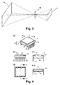
- Fig. 3 shows on the basis of a schematic sketch the relationship between the object plane 9 and image plane 11.
- a lens is a lens system 10, which collects incident light and generates a projection of an object plane 9 on the image plane 11.
- An electronic subassembly is a component that consists of a printed circuit board and electronic components.
- electronic assemblies are e.g. used to perform the function of converting the incident light into electronic signals.
- the printed circuit board serves as a mechanical support and for electrical contacting and connection of the electronic components.
- Printed circuit boards have a top side and a bottom side. The top is usually referred to as the top page, the bottom usually called the bottom side. Determining which side is up and which down can be purely arbitrary.
- Electronic components can be mounted on both the top and the bottom side.
- As a mounting placeholder for electronic components structures are provided on the circuit board, referred to by those skilled in the art as so-called footprints.
- the electronic components are electrically interconnected on the printed circuit board by means of conductor tracks in the desired functionality.
- the electronic components are functional elements which perform partial tasks in an electronic module (eg resistors, inductors, capacitors, integrated circuits). By combining many electronic components, the desired functionality is achieved in conjunction with the printed circuit board. In addition to being distinguishable in terms of their function, electronic components can also be differentiated by the type of mounting method on the printed circuit board. In general, a distinction is made between surface-mounted components (abbreviation: "SMD” for Surface Mounted Device) and wired components (abbreviation: "THD” for Through Hole Device). THD components are housing types with several Wire connections. A footprint for a THD device consists of one via per wire connection.
- SMD Surface Mounted Device
- THD Through Hole Device
- a through-hole is a sleeve inserted into the printed circuit board with a hole in the middle.
- THD components are inserted into the through-contacts of the printed circuit board in a preparatory step and fixed there until they are actually mounted.
- SMD components have pads instead of wire connectors.
- a footprint for an SMD component consists of copper pads located on the top or bottom side of the PCB.
- a subcomponent of the electronic module is the printed circuit board. On the circuit board, electronic components are mounted on one side (top or bottom side) or on both sides (top and bottom side). If an electronic module only has SMD components, this is an SMD module. If an electronic module has only THD components, this is called a THD module. If an electronic assembly consists of at least one SMD component and of at least one THD component, this is referred to as a mixed assembly.
- Image sensors are available in SMD and THD packages.
- Fig. 4 shows a typical image sensor with a THD package shape in perspective view (a), view from the left (b), view from the front (c), view from above (d) and a sectional view (AA) through the sensor along the in Fig. 4 (d) shown section line.
- the THD image sensor consists of an image sensor housing 12 and a plurality of wire terminals 13.
- the wire terminals 13 are usually designed as solderable Randähnchen with rectangular cross-section.
- the most important component of the THD image sensor is the electronic circuit integrated on semiconductor material, the so-called chip or Die 16.
- the Die 16 contains, among other things, the optically active surface, which collects incident light and converts the light into electronic signals.
- the image sensor is supplied with the necessary energy for operation.
- the image sensor is usually provided with a cover glass 14.
- image sensor reference positions are provided. Image sensor reference positions, but also, for example, position information and deviations can be described according to the Cartesian coordinate system by three spatial directions in the X direction 99, Y direction 100 and Z direction 101. Accordingly, the image sensor reference positions 15, 19, and 58 can be assigned to the X, Y, and Z directions, respectively.
- Fig. 5 11 shows a view (e) of the opened camera as viewed from above and a sectional view (BB) along the section line shown in view (e) with the optical beam path of the camera when the object plane 9 is projected onto the optically sensitive surface of the die 16 of the image sensor.
- the optical projection of the object plane 9 onto an image plane 11 takes place by means of a lens 4 Fig. 5 the lens 4 is mounted on the camera housing carrier 1.
- the printed circuit board 5 of the image sensor module is fastened, for example, by means of screws 17 to the housing carrier 1.
- the mounting of a THD image sensor can be done in different ways.
- the image sensor is soldered to a circuit board 5 and is thus part of an electronic assembly, which is referred to as an image sensor assembly.
- the image sensor housing 12 is aligned with the printed circuit board 5.
- the assembly of the image sensor module consisting of the printed circuit board 5 and the THD image sensor, takes place on the housing carrier 1 of the camera.
- the assembly housing carrier 1 is aligned.
- the alignment can also be done by means of constructive measures. Since the objective 4 is also aligned with the housing carrier 1, an alignment of the image plane 11 with the optically sensitive area of the die 16 is then present.
- the alignment of a THD image sensor on the circuit board 5 is usually done using a Hilfstechnikmaschines.
- the circuit board is placed in the auxiliary tool.
- the auxiliary tool allows the adjustment of the circuit board so that it lies in an aligned and reproducible exact position in the auxiliary tool. This position corresponds to the later mounting state on the housing support 1 of the camera.
- the THD image sensor is inserted into the plated-through holes of the THD footprint of the printed circuit board 5.
- the auxiliary tool aligns the THD image sensor with the printed circuit board 5 by means of the reference position 15 in the X direction, the reference position 19 in the Y direction and the reference position 58 in the Z direction. After adjustment of the image sensor with respect to the circuit board 5, the image sensor is fixed and soldered to the circuit board 5.
- the mounting of the THD image sensor on the circuit board 5 as part of a digital industrial camera while requesting a faultless alignment of the optically sensitive surface of the Dies 16 to the optical image plane 11 as a projection of the object plane 9 is associated with disadvantages.
- Image sensors in a THD package form are attached by default to a circuit board by the soldering assembly method.
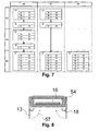
- Fig. 7 shows a tabular listing of the manufacturing processes for producing a module with THD image sensor.
- SMD manufacturing process 27 consists of a pasting 28 of the image sensor assembly with solder paste, a component 29 with SMD components and a subsequent reflow soldering 30.
- the paste 28, the assembly 29 and the reflow soldering 30 are Automated Manufacturing Process Steps 24.
- a typical THD image sensor THD manufacturing process 31 consists of preparing 32 the wire connections of the THD image sensor. This includes, for example, shortening the image sensor wire connections 13. Subsequently, the THD image sensor is placed on the image sensor assembly 33.
- the alignment 34 and fixation 35 of the THD image sensor 21 then takes place on the printed circuit board of the image sensor assembly by means of an auxiliary tool. Thereafter, the THD image sensor is soldered by hand soldering or wave soldering 36 to the circuit board. In the last step, the auxiliary tool is removed from the image sensor assembly 37.
- the auxiliary tool is removed from the image sensor assembly 37.
- soldering process 36 Only the actual soldering process 36 can be performed as a manual or automated manufacturing process step 26.
- wave soldering the soldering process becomes the automated manufacturing process step 24. In the case of manual soldering, it is a manual manufacturing process step 25.
- Fig. 7 There are different configurations of an image sensor module. Thus, a distinction is made between the one-sided SMD-populated module 41 and the both-sided SMD-populated module 40 in the mix-equipped image sensor modules.
- the one-sided SMD-equipped image sensor module 41 is for equipping the first SMD processing page 43 of the SMD manufacturing process Go through 27 times.
- a double-sided SMD-equipped image sensor assembly 40 of the SMD manufacturing process 27 is passed once each for the first SMD processing page 43 and once for the second SMD processing page 44.
- an image sensor assembly in which all components are THD components, including the THD image sensor 21 one speaks of a pure THD module 42. This eliminates all SMD processing steps.
- the mixed-use image sensor assemblies 40 and 41 contain several manufacturing process steps, other manufacturing process steps 38 occur between the manufacturing process steps. This acts it is the intermediate storage 39 of the partially assembled image sensor assembly.
- the partially mounted image sensor assemblies are provided, for example, in boxes for the next manufacturing step.
- the THD manufacturing process 31 consists predominantly of manual manufacturing process steps 25, which are expensive and with the exception of the actual THD soldering process 36 only with great effort automate. This leads to higher production costs compared to an automated process. Furthermore, the THD manufacturing process 31 includes many individual substeps as compared to an SMD manufacturing process 27. However, a large number of sub-steps leads to a higher production cost compared to a smaller number. The combination of SMD manufacturing process 27 and subsequent THD manufacturing process 31 leads to a mere SMD manufacturing process 27 to longer production times and thus in turn to higher manufacturing costs. In the other manufacturing process steps 38 are generally non-value-added, manual manufacturing process steps 25. Between the last SMD manufacturing process 27 and the THD manufacturing process 31 for processing the THD image sensor such another manufacturing process step 38 is required, which also leads to increased manufacturing costs for the image sensor assembly.
- the object of the invention is to provide an image sensor assembly as well as a production method and auxiliaries which enable smaller dimensions, more efficient production and higher process reliability and reproducibility.
- a modified THD image sensor whose wire connections are modified by means of a suitable bending tool such that the wire connections do not have to be inserted and soldered through the circuit board and that they form a reference to an optically sensitive surface of the image sensor.
- the modified THD image sensor can thus be equipped in an SMD manufacturing process.
- the modified THD image sensor can thus be mounted in an SMD manufacturing process, the manufacturing method comprising the partial aspects of modification of the THD image sensor and processing of the modified THD image sensor in the SMD manufacturing process.
- the modified wire terminals of the image sensor may be J-shaped. But you can also have a Gull Wing shape or other suitable for surface mounting form.
- bending is to be understood to mean any forming production process or processes that transform a starting material by modifying a shape change.
- the type of modification may vary depending on the method. Common technical methods are e.g. Mechanical bending or bending by laser.
- mechanical bending a force in the form of a mechanical bending moment is exerted on the starting material. This force leads to a plastic deformation.
- the starting material is locally heated by laser for a short time. The heating and subsequent cooling of the material leads to tension within the material, which then also leads to a plastic deformation.
- the modified wire connections of the image sensor may have different lengths, so that a predetermined inclination of the image sensor relative to an object plane of the camera can be achieved.
- the length of the modified wire connections of the image sensor can be selected as a function of an optical filter in the beam path of the camera.
- the printed circuit board can have a connection pattern on the surface, which has an electrically conductive contact surface for surface mounting for each modified wire connection of the image sensor.
- the image sensor assembly according to the invention can be fixed to a camera housing carrier of a digital industrial camera.
- alignment and fixing of the image sensor and execution of the bending process can be provided as a function of the position of the optically sensitive surface of the image sensor.
- the alignment can be carried out using at least one mechanical stop for determining at least one reference position, wherein the fixing can be effected by mechanical clamping of the image sensor housing against a bending tool.
- the alignment means of the bending tool can have at least one mechanical stop associated with a reference position for the optically sensitive surface of the image sensor.
- the fixing means may comprise at least two jaws.
- the alignment can also be based on an optical measurement of the optically sensitive surface of the image sensor.
- the alignment means of the bending tool may comprise an optical measuring system which detects the position of the optically sensitive surface of the image sensor within the image sensor housing.
- the modification of the original wire connections can preferably also be used for the correction of tolerance values in at least one spatial direction.
- the modification of the THD image sensor includes the steps of aligning and fixing the THD image sensor on the bending tool and modifying the wire connections of the THD image sensor.
- the modification of the wire connections takes place, for example, depending on the position of the optically sensitive surface of the image sensor dies. For this reason, the THD image sensor is aligned before the modification to the bending tool in three-dimensional space and fixed after alignment in the bending tool.
- the alignment of the THD image sensor to the bending tool can be done mechanically or optically.
- the optically sensitive surface of the image sensor dies is aligned with the externally accessible image sensor reference positions in the X direction, Y direction and Z direction.
- the image sensor reference positions of the THD image sensor in X-direction, Y-direction and Z-direction can be used as a mechanical stop and the THD image sensor can be aligned to the tool via these positions.
- Laying the image sensor housing flat in the Z direction avoids the image sensor tilt.
- the THD image sensor is mechanically fixed in the bending tool.
- An example of a possible fixation is the mechanical clamping of the image sensor housing against the bending tool.
- FIG. 12 shows an exemplary modification of the wire terminals 13 of a THD image sensor 54 according to a first embodiment with optical alignment of the THD image sensor 54 to the bending tool (not shown).
- the optically sensitive area of the die 16 of the THD image sensor 54 is aligned, fixed and fixed during the manufacturing process to the externally accessible image sensor reference positions in the X direction, Y direction and Z direction, this manufacturing process is subject to certain tolerances.
- Typical tolerance values for the X, Y and Z directions are +/- 100pm, for the +/- 1 degree rotation and for the +/- 0.5 degree tilt.
- the THD image sensor 54 In order to achieve even higher accuracies in the alignment of the THD image sensor 54 relative to the mechanical alignment to the bending tool, it is possible, instead of the mechanical stops, to directly measure the position of the optically sensitive surface of the image sensor dies 16 in three-dimensional space.
- the measurement can take place by means of an optical system which determines the position of the optically sensitive surface of the image sensor dies 16 through the cover glass and, according to the measurement result, aligns the THD image sensor 54 with the bending tool in three-dimensional space. After aligning the THD image sensor to the bending tool, the THD image sensor is mechanically fixed in the bending tool.
- FIG Fig. 8 An example of a possible modification is shown in FIG Fig. 8 shown.
- a substantially circular bending movement 57 is carried out on a circular path.
- the originally formed image sensor wire terminals 13 are transformed into modified image sensor wire terminals 18.
- Fig. 8 leads the modification by the bending movement shown 57 to a modified THD image sensor 54 with so-called J-shaped wire terminals 18, as they are, for example, in IPC J-STD-001 D DE, "Requirements for Brazed Electrical and Electronic Assemblies", February 2005, Chapter 7.6.9, page 27 are described.
- the optically sensitive surface of the image sensor dies 16 is adjusted to outside accessible reference positions in the X direction, Y direction, and Z direction during manufacture of the THD image sensor and inside the Image sensor housing firmly mounted.
- the relationship between the optically sensitive area of the image sensor dies 16 and the position of the image sensor wire terminals 13 is secondary to this for the image sensor manufacturer, since the orientation, fixation and soldering of the conventional THD image sensor on a Image sensor assembly is done by default using auxiliary tool.
- the position of the image sensor wire terminals 13 with respect to the optically sensitive surface of the image sensor Dies 16 is usually subject to certain tolerances.
- Typical tolerance values for the X and Y directions are disadvantageously too high at +/- 100 ⁇ m. In order to allow an optimal alignment of the modified THD image sensor 54 to the printed circuit board by a subsequent SMD manufacturing process, it is exactly these too high tolerance values due to the bending process that are disadvantageous.
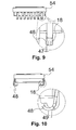
- Fig. 9 shows a modification of the wire terminals of the modified THD image sensor according to the first embodiment with correction of the tolerance values in the X direction.
- the correction of the tolerance value for the X-direction takes place by bending a tolerance-related modified wire connections 46 laterally with respect to a modified wire connection 18, in which no correction of the tolerance value is necessary.
- the position of the optically active area of the image sensor die 16 with respect to the soldering area of the modified wire terminals 18 is corrected by a correction value 47 in the X direction, which is referred to herein as ⁇ X.
- Fig. 10 shows a modification of the wire terminals of the modified THD image sensor according to the first embodiment with correction of the tolerance values in the X direction.
- the correction of the tolerance value for the Y-direction is carried out by laterally bending a tolerance-sensitive modified wire connection 48 with respect to a modified wire connection 18, in which no correction of the tolerance value is necessary.
- the position of the optically active area of the image sensor die 16 with respect to the soldering area of the modified wire terminals 18 is corrected by a correction value 49 in the Y direction, which is referred to herein as ⁇ Y.
- Fig. 11 shows a modification of the wire terminals of the modified THD image sensor according to the first embodiment with correction of the tolerance values in the Z direction.
- the correction of the tolerance value for the Z-direction by changing the wire connection length of a tolerance-sensitive modified wire connection 50 against a modified wire connection 18, in which no correction of the tolerance value is necessary.
- the position of the optically active surface of the image sensor dies 16 with respect to the soldering area of the modified wire terminals 18 is corrected by a correction value 51 in the Z direction, which is denoted here as ⁇ Z.
- a modified image sensor 54 whose modified image sensor wire connections 18 serve as a reference position with respect to the optically sensitive area of the image sensor die 16, thus results.
- a universal bending tool can be used, which can fulfill the bending task regardless of the conditions on the later image sensor assembly.
- the use of the universal bending tool compared to several adapted to the respective image sensor assembly tools benefits in that only a single design task (instead of recurring design task) and thus a low production costs incurred because the universal bending tool can be used across products.
- material, maintenance, evaluation and parts costs can be reduced, since instead of many different customized auxiliary tools only a universal bending tool needs to be set up, maintained, tested and repaired. This also leads to a faster product development and thus a faster time-to-market for the digital industrial camera, because after a single completion of the universal bending tool for all subsequent products this design task is omitted in the context of product development.
- a variation of ⁇ Z can be used to compensate for optical path differences.
- Image sensors are generally differentiated into monochrome image sensors and color image sensors. While monochrome image sensors convert incident light into achromatic images, color image sensors produce an image composed of multiple colors, such as red, green, and blue. For this, the image sensor requires a plurality of color masks, which are transparent in predetermined parts of the visible wavelength range. Since the currently available color masks are also transparent in the near-infrared wavelength range, a so-called infrared cut filter may be required to prevent disadvantageous color errors, which prevents light from the near-infrared wavelength range from reaching the photosensitive surface of the sensor.
- Fig. 12 shows a schematic representation of an exemplary modification of the wire terminals of a THD image sensor according to a second embodiment for compensating different optical paths when using infrared cut filters (IR cut filters).
- IR cut filters infrared cut filters
- this unwanted optical path length difference ( ⁇ Z) 51 can now be compensated in a constructive manner as a shift of the image plane.
- An example of this is the design and manufacture of several different auxiliary tools for image sensors with and without the use of an infrared barrier filter 72.
- Another example of a constructive measure is the design and manufacture of different camera housing carrier, which in the attachment of the image sensor assembly also the Path length difference (.DELTA.Z) 51 can compensate.
- both constructive measures lead to disadvantageous costs, because the number of auxiliary tools or camera housing support types required is increased.
- the inventive modification of the image sensor wire connections and the subsequent processing in a SMD manufacturing process can be according to Fig.
- a variation of the image sensor tilt and ⁇ Z may be used to compensate for an oblique viewing or viewing angle.
- a high-rise is mentioned here. Now, with the digital industrial camera in an oblique viewing position, e.g. on the ground floor, you have to pan the industrial camera so that the entire object is within the field of view of the industrial camera.
- Fig. 13 shows a schematic representation of an exemplary modification of the wire connections of a THD image sensor according to a third embodiment in an industrial camera 75 with different optical distances in the application of skyscraper.
- an object plane 9 orthogonal to the viewing direction would be projected onto an image plane 11.
- the orthogonally stationary object plane 9 does not coincide with the actual object plane 77.
- this skewing has the consequence that only a small area, which can be described as a focus point 78, has the necessary sharpness of image. All other areas of the actual object plane 77 are unfavorably reproduced in the image blurred. The cause of this blur are optically different lengths of travel.
- the optical path between the lower end 96 of the object plane 77 and the image plane 11 can be characterized as short, the optical path between the uppermost end 97 of the object plane 77 and the image plane 11 results in an optically long path.
- the difference between the two optical paths can now be compensated by a consciously induced variation of the tilt or inclination of the THD image sensor 76.
- one row of the image sensor wire terminals is bent at a greater distance from the circuit board 5 than the other row of the image sensor wire terminals.
- the modified wire connections for the Y-direction path length difference and the image sensor tilt can be used to provide a specially adapted modified image sensor 76 which can eliminate the technical disadvantages of blurring the image on a printed circuit board 5 of the image sensor assembly.
- This solution is advantageous for the aforementioned reasons compared to the use of a special Hilfstechnikmaschines.
- Fig. 14 shows a schematic representation of the assembly of the modified THD image sensor 54 on a printed circuit board 5.
- an SMD footprint (SMD) 55 is provided on the circuit board 5 of the image sensor module.
- This connection pattern 55 here consists of a copper pad (copper pad) 56 for each modified image sensor wire connection.
- the copper pads 56 have no holes and are located with respect to the printed circuit board 5 on the mounting side of the modified image sensor 54.
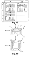
- Fig. 15 shows a tabular overview of the manufacturing processes when processing the modified THD image sensor. Compared to Fig. 7 shows Fig. 15 now a much leaner manufacturing process sequence.
- the modified image sensor can now be processed in the SMD manufacturing process 27 due to the modifications. Since the THD image sensor is often the only THD component of the image sensor module, it eliminates all THD manufacturing processes and also the assembly variant of an image sensor module equipped exclusively with THD components. From the assembly variant mischbe Publishedte assembly with one-sided populated SMD components is then a mounting variant with one-sided populated SMD components 60.
- the SMD production process 27 will be processed twice on both sides of assembled SMD assemblies 59 for equipping the first SMD processing side 43 and for subsequent loading of the second SMD processing side 44.
- another manufacturing process step 38 which includes the manual process step 25 of the intermediate storage of the partially mounted image sensor modules 39.
- unilaterally equipped SMD module 60 eliminates the processing of the second SMD processing page 44 and thus also the other manufacturing process 38 for temporary storage of the image sensor assemblies 39.
- the assembly of the first SMD processing page 43 is preceded by the component preparation 52.
- This is another manufacturing process 38 which includes the manual process step 25 of the modification of the THD image sensor 53.
- the processing of the modified image sensor in the SMD production process 27 does not result in any changes to the production process itself.
- the SMD production process 27 continues to consist of paste 28 of the image sensor assembly with solder paste, the assembly 29 with SMD components and the subsequent reflow Solder 30 together.
- Beep 28, assembly 29, and reflow soldering 30 are automated manufacturing process steps 24.
- the modified image sensor is treated like an SMD component, it is now possible to realize automated assembly and soldering.
- automated assembly it is possible to use machines with optical measuring systems which can center and accurately equip the modified image sensor on the basis of the modified image sensor wire connections. Since the modified image sensor wire connections produce a reference to the optically sensitive surface of the image sensor dies 16, an automated alignment of the modified image sensor with the image sensor assembly can thus already take place during assembly. In the following reflow soldering, the modified image sensor is then soldered to the image sensor assembly.
- the modified image sensor By processing the modified image sensor in an SMD manufacturing process, there are advantages in that the total space requirement is reduced due to the possible use of an SMD connection pattern, since no THD vias and no additional mounting clearances for soldering iron or wave soldering are necessary and thus additional space for the assembly of other components can be used.
- the thus reduced printed circuit board leads to manufacturing advantages and the THD manufacturing process for the THD image sensor can be saved, so that a slimmer production process is possible.
- Other manufacturing process steps e.g., temporary storage of the partially mounted image sensor assemblies
- the change in the principle of alignment of the THD image sensor to the image sensor assembly due to the SMD manufacturing process leads to an increase in process reliability and reproducibility due to increased accuracy by using optical measuring systems of the placement machines and increased accuracy by using the self-centering effect during the reflow soldering ,
- the modification of the THD image sensor can be carried out by means of a bending tool in three sub-steps alignment, fixation and modification.
- Fig. 16 shows a schematic side view (top) and top view (bottom) of a mechanical alignment of a THD image sensor 89 in a bending tool according to a first embodiment with mechanical alignment.
- a part for aligning the THD image sensor 89 with respect to the bending tool consists of an upper part 83 and a lower part 82.
- the THD image sensor 89 is inserted into the lower part 82 and mechanically, for example by means of mechanical springs 88, to mechanical stops 84 pressed.
- These mechanical stops 84 are located directly on the image sensor reference positions in the X direction and Y direction and thus form a direct reference to the optically active surface of the image sensor dies 16.
- the upper part 83 is then placed on the lower part 82 and fixed mechanically, eg by clamping or screwing.
- the upper part 83 also has mechanical springs 88 and thus presses the THD image sensor 89 from above onto a reference surface 58, so that now a mechanical orientation 79 in the X direction, a mechanical orientation 80 in the Y direction and a mechanical orientation 81 in FIG Z direction of the THD image sensor 89 is achieved with respect to the bending tool.
- Fig. 17 shows a schematic side view (top) and top view (bottom) of a fixation and modification of the THD image sensor 89 in a bending tool according to a second embodiment with optical alignment.
- the fixation of the THD image sensor 89 takes place in the bending tool.
- two clamping jaws 86 can be guided by a horizontal traversing movement 85 to the aligned THD image sensor 89, which in the end position fix the THD image sensor 89 in its aligned position within the bending tool.
- the sequence of sub-steps for the modification of the image sensor wire connections 13 changes.
- the procedure according to FIG Fig. 17 First, the fixation of the THD image sensor 89 in the bending tool by means of the jaws 86. After fixing, the optical alignment takes place.
- an optical measuring system 95 may be provided which detects the position of the optically active surface of the image sensor dies 16 within the image sensor housing.
- the orientation of the THD image sensor 89 to the bending tool is now carried out by means of technically familiar means, eg with a motor-driven linear displacement unit.
- a position correction of the THD image sensor 89 in the X direction 91, Y direction 92 and Z direction 93 is performed. It can be provided that in the sense of a control loop, the orientation is changed in such a way that on
- a correction of the image sensor tilt 90 and a rotation 94 can be performed by changing the slope and the rotation with technically common means such that a match of the actual value is achieved with a target value.
- THD image sensor 89 After the alignment and fixation in the mechanical or the fixation and alignment in the optical case, there is now a fixed THD image sensor 89, which is located within the bending tool in a defined position. Depending on the application, variations in the position of the THD image sensor 89 in the bending tool in the X direction 91, Y direction 92, Z direction 93, image sensor tilt 90 and rotation 94 can now be performed, for example.
- the modification of the original image sensor wire terminals 13 takes place.
- the fixed and aligned THD image sensor 89 with its image sensor wire terminals 13 is fed to a bending mechanism 87.
- the bending mechanism 87 leads in the case of Fig. 17 a circular bending movement 57, which leads to the modified image sensor wire connection form.
- the modified THD image sensor 89 is removed from the bending tool and can subsequently be processed in the SMD production process.
- an image sensor assembly for a camera preferably a digital industrial camera, with a printed circuit board and one or more electronic components, a method for their preparation and a bending tool
- at least one of the components is a modified THD image sensor, which by means of a adapted bending tool has modified image sensor wire connections, which are mounted by a manufacturing process on the surface of the circuit board, so that the wire connections do not have to be inserted and soldered through the circuit board, and that they form a reference to an optically sensitive surface of the image sensor.
- the modified THD image sensor can thus be equipped in an SMD production process.
- the proposed alternative solutions according to the embodiments can be used in connection with a variety of image recording devices and cameras, in which a module with THD image sensor is used.
- the modification of the wire terminals is not limited to the above-described embodiments.
- Various bending or other modification forms as well as alternative bending methods of the wire terminals may be provided to enable surface mounting of the THD image sensor in the present invention.
Landscapes
- Engineering & Computer Science (AREA)
- Multimedia (AREA)
- Signal Processing (AREA)
- Microelectronics & Electronic Packaging (AREA)
- Studio Devices (AREA)
Priority Applications (1)
| Application Number | Priority Date | Filing Date | Title |
|---|---|---|---|
| EP12003735.3A EP2663070A1 (fr) | 2012-05-10 | 2012-05-10 | Composant de capteur d'images pour une caméra, ainsi que procédé et outil de pliage pour sa fabrication |
Applications Claiming Priority (1)
| Application Number | Priority Date | Filing Date | Title |
|---|---|---|---|
| EP12003735.3A EP2663070A1 (fr) | 2012-05-10 | 2012-05-10 | Composant de capteur d'images pour une caméra, ainsi que procédé et outil de pliage pour sa fabrication |
Publications (1)
| Publication Number | Publication Date |
|---|---|
| EP2663070A1 true EP2663070A1 (fr) | 2013-11-13 |
Family
ID=46085326
Family Applications (1)
| Application Number | Title | Priority Date | Filing Date |
|---|---|---|---|
| EP12003735.3A Withdrawn EP2663070A1 (fr) | 2012-05-10 | 2012-05-10 | Composant de capteur d'images pour une caméra, ainsi que procédé et outil de pliage pour sa fabrication |
Country Status (1)
| Country | Link |
|---|---|
| EP (1) | EP2663070A1 (fr) |
Cited By (4)
| Publication number | Priority date | Publication date | Assignee | Title |
|---|---|---|---|---|
| CN105763781A (zh) * | 2016-04-12 | 2016-07-13 | 深圳市赋兴光电有限公司 | 摄像头生产方法 |
| CN108231914A (zh) * | 2016-12-20 | 2018-06-29 | 3D加公司 | 3d成像光电模块 |
| DE102021112292A1 (de) | 2021-05-11 | 2022-11-17 | Audi Aktiengesellschaft | Verfahren zum Herstellen einer elektronischen Anordnung |
| DE102016000078B4 (de) | 2016-01-07 | 2023-08-17 | Ic-Haus Gmbh | Verfahren zur Herstellung einer elektronischen Baugruppe, elektronische Baugruppe und Verfahren zur Montage einer elektronischen Baugruppe |
Citations (7)
| Publication number | Priority date | Publication date | Assignee | Title |
|---|---|---|---|---|
| JPH0715180A (ja) * | 1993-06-25 | 1995-01-17 | Toshiba Corp | リード付き部品の表面実装方法 |
| US6156587A (en) * | 1998-03-02 | 2000-12-05 | Fuji Photo Film Co., Ltd. | Method of attaching solid state imaging device |
| JP2001085897A (ja) * | 1999-09-16 | 2001-03-30 | Fuji Electric Co Ltd | 電子部品の加工装置 |
| JP2002009264A (ja) * | 2000-06-19 | 2002-01-11 | Chinon Ind Inc | 固体撮像素子および撮像装置 |
| US20020154239A1 (en) * | 2001-04-24 | 2002-10-24 | Hisayoshi Fujimoto | Image sensor module and method of making the same |
| GB2404517A (en) * | 2003-07-29 | 2005-02-02 | Pentax Corp | Aligning image sensor package in camera. |
| EP2112538A1 (fr) * | 2008-04-25 | 2009-10-28 | Hitachi, Ltd. | Unité de caméra |
-
2012
- 2012-05-10 EP EP12003735.3A patent/EP2663070A1/fr not_active Withdrawn
Patent Citations (7)
| Publication number | Priority date | Publication date | Assignee | Title |
|---|---|---|---|---|
| JPH0715180A (ja) * | 1993-06-25 | 1995-01-17 | Toshiba Corp | リード付き部品の表面実装方法 |
| US6156587A (en) * | 1998-03-02 | 2000-12-05 | Fuji Photo Film Co., Ltd. | Method of attaching solid state imaging device |
| JP2001085897A (ja) * | 1999-09-16 | 2001-03-30 | Fuji Electric Co Ltd | 電子部品の加工装置 |
| JP2002009264A (ja) * | 2000-06-19 | 2002-01-11 | Chinon Ind Inc | 固体撮像素子および撮像装置 |
| US20020154239A1 (en) * | 2001-04-24 | 2002-10-24 | Hisayoshi Fujimoto | Image sensor module and method of making the same |
| GB2404517A (en) * | 2003-07-29 | 2005-02-02 | Pentax Corp | Aligning image sensor package in camera. |
| EP2112538A1 (fr) * | 2008-04-25 | 2009-10-28 | Hitachi, Ltd. | Unité de caméra |
Non-Patent Citations (3)
| Title |
|---|
| "IPC J-STD-001 D DE", February 2005, article "Anforderungen an gelötete elektrische und elektronische Baugruppen", pages: 25 |
| "IPC J-STD-001 D DE", February 2005, article "Anforderungen an gelötete elektrische und elektronische Baugruppen", pages: 27 |
| "Wolf-Dieter Schmidt", article "Grundlagen der Leiterplatten-Baugruppen-Entwicklung und Fertigung", pages: 125 - 126 |
Cited By (5)
| Publication number | Priority date | Publication date | Assignee | Title |
|---|---|---|---|---|
| DE102016000078B4 (de) | 2016-01-07 | 2023-08-17 | Ic-Haus Gmbh | Verfahren zur Herstellung einer elektronischen Baugruppe, elektronische Baugruppe und Verfahren zur Montage einer elektronischen Baugruppe |
| CN105763781A (zh) * | 2016-04-12 | 2016-07-13 | 深圳市赋兴光电有限公司 | 摄像头生产方法 |
| CN108231914A (zh) * | 2016-12-20 | 2018-06-29 | 3D加公司 | 3d成像光电模块 |
| CN108231914B (zh) * | 2016-12-20 | 2023-01-31 | 3D加公司 | 3d成像光电模块 |
| DE102021112292A1 (de) | 2021-05-11 | 2022-11-17 | Audi Aktiengesellschaft | Verfahren zum Herstellen einer elektronischen Anordnung |
Similar Documents
| Publication | Publication Date | Title |
|---|---|---|
| DE69711043T2 (de) | Vorrichtung und verfahren zum siebdrucken | |
| DE112017007030B4 (de) | Substratuntersuchungsvorrichtung | |
| DE602005000512T2 (de) | Verfahren und vorrichtung zum montieren von bauelementen | |
| DE112007002181T5 (de) | Vorrichtung zur Herstellung von mit Bauteilen bestückten Leiterplatten und Verfahren zur Positionssteuerung von elektronischen Bauteilen in einer Vorrichtung zur Herstellung von mit Bauteilen bestückten Leiterplatten | |
| DE69109137T2 (de) | Oberflächenmontage-Verfahren und Vorrichtung. | |
| EP1110439B1 (fr) | Procede et dispositif pour etalonner un deplacement et/ou une position angulaire d'un systeme de retenue dans un dispositif destine a produire des blocs de composants electriques et substrat d'etalonnage | |
| DE112017007435T5 (de) | Komponentenbestückungssystem und klebemitteluntersuchungsvorrichtung | |
| WO2016124184A1 (fr) | Module de caméra et procédé de fabrication | |
| DE10296416T5 (de) | Verfahren und Vorrichtung zur Registrierungssteuerung in der Produktion durch Belichten | |
| EP2663070A1 (fr) | Composant de capteur d'images pour une caméra, ainsi que procédé et outil de pliage pour sa fabrication | |
| DE60106978T2 (de) | Verfahren zur Herstellung eines Leiterplattenmoduls | |
| DE69605103T2 (de) | Bestückungsautomat für bauelemente | |
| DE102005053202A1 (de) | Vorrichtung zum Vorbereiten einer Mehrschicht-Leiterplatte auf das Bohren von Kontaktierungsbohrungen | |
| DE602004009982T2 (de) | Metallschablone und Verfahren zum Drucken von bleifreier Lötpaste mit derselben | |
| DE112017007027B4 (de) | Lotdruckuntersuchungsvorrichtung | |
| EP0307766A1 (fr) | Circuit imprimé permettant le montage de composants SMD | |
| EP2983458B1 (fr) | Procede de fixation d'une source lumineuse semi-conductrice smd sur une carte de circuits imprimes d'un phare de vehicule automobile | |
| EP2989871A1 (fr) | Dispositif de placement et procédé de placement permettant d'orienter dans la bonne position un substrat et/ou de l'équiper d'un composant | |
| EP3997968B1 (fr) | Procédé pour retirer un composant installé sur une carte de circuits imprimés | |
| EP1606981A2 (fr) | Procede et dispositif d'alignement d'un substrat et d'un gabarit d'impression lors d'une impression de pate de brasage | |
| DE10214817B4 (de) | Anordnung zur Höhenmessung des Lotpastenauftrages | |
| DE112020001298T5 (de) | Bauteilmontagevorrichtung und Bauteilmontageverfahren, Montagesubstrat-Herstellungssystem und Montagesubstrat-Herstellungsverfahren, und Montiertes-Bauteil-Prüfvorrichtung | |
| DE102020115598B3 (de) | Verfahren und Bestückmaschine zum Bestücken von Bauelementeträgern basierend auf einem Rekalibrieren der Bestückmaschine im realen Bestückbetrieb, Computerprogramm zum Steuern einer Bestückmaschine | |
| DE10335312A1 (de) | Erstellen von Testmustern zur Nachkontrolle | |
| DE102019129971A1 (de) | Verfahren zum Auflöten eines Bauelements auf eine Leiterplatte, Elektronikeinheit und Feldgerät der Automatisierungstechnik |
Legal Events
| Date | Code | Title | Description |
|---|---|---|---|
| PUAI | Public reference made under article 153(3) epc to a published international application that has entered the european phase |
Free format text: ORIGINAL CODE: 0009012 |
|
| AK | Designated contracting states |
Kind code of ref document: A1 Designated state(s): AL AT BE BG CH CY CZ DE DK EE ES FI FR GB GR HR HU IE IS IT LI LT LU LV MC MK MT NL NO PL PT RO RS SE SI SK SM TR |
|
| AX | Request for extension of the european patent |
Extension state: BA ME |
|
| STAA | Information on the status of an ep patent application or granted ep patent |
Free format text: STATUS: THE APPLICATION IS DEEMED TO BE WITHDRAWN |
|
| 18D | Application deemed to be withdrawn |
Effective date: 20140514 |