EP2665101B1 - Procédé de fabrication d'un transistor LDMOS haute tension - Google Patents
Procédé de fabrication d'un transistor LDMOS haute tension Download PDFInfo
- Publication number
- EP2665101B1 EP2665101B1 EP12167851.0A EP12167851A EP2665101B1 EP 2665101 B1 EP2665101 B1 EP 2665101B1 EP 12167851 A EP12167851 A EP 12167851A EP 2665101 B1 EP2665101 B1 EP 2665101B1
- Authority
- EP
- European Patent Office
- Prior art keywords
- well
- drift region
- region
- conductivity
- type
- Prior art date
- Legal status (The legal status is an assumption and is not a legal conclusion. Google has not performed a legal analysis and makes no representation as to the accuracy of the status listed.)
- Not-in-force
Links
Images
Classifications
-
- H—ELECTRICITY
- H10—SEMICONDUCTOR DEVICES; ELECTRIC SOLID-STATE DEVICES NOT OTHERWISE PROVIDED FOR
- H10D—INORGANIC ELECTRIC SEMICONDUCTOR DEVICES
- H10D62/00—Semiconductor bodies, or regions thereof, of devices having potential barriers
- H10D62/10—Shapes, relative sizes or dispositions of the regions of the semiconductor bodies; Shapes of the semiconductor bodies
- H10D62/13—Semiconductor regions connected to electrodes carrying current to be rectified, amplified or switched, e.g. source or drain regions
- H10D62/149—Source or drain regions of field-effect devices
- H10D62/151—Source or drain regions of field-effect devices of IGFETs
- H10D62/156—Drain regions of DMOS transistors
- H10D62/157—Impurity concentrations or distributions
-
- H—ELECTRICITY
- H10—SEMICONDUCTOR DEVICES; ELECTRIC SOLID-STATE DEVICES NOT OTHERWISE PROVIDED FOR
- H10D—INORGANIC ELECTRIC SEMICONDUCTOR DEVICES
- H10D30/00—Field-effect transistors [FET]
- H10D30/01—Manufacture or treatment
- H10D30/021—Manufacture or treatment of FETs having insulated gates [IGFET]
- H10D30/0221—Manufacture or treatment of FETs having insulated gates [IGFET] having asymmetry in the channel direction, e.g. lateral high-voltage MISFETs having drain offset region or extended-drain MOSFETs [EDMOS]
-
- H—ELECTRICITY
- H10—SEMICONDUCTOR DEVICES; ELECTRIC SOLID-STATE DEVICES NOT OTHERWISE PROVIDED FOR
- H10D—INORGANIC ELECTRIC SEMICONDUCTOR DEVICES
- H10D30/00—Field-effect transistors [FET]
- H10D30/60—Insulated-gate field-effect transistors [IGFET]
- H10D30/601—Insulated-gate field-effect transistors [IGFET] having lightly-doped drain or source extensions, e.g. LDD IGFETs or DDD IGFETs
- H10D30/603—Insulated-gate field-effect transistors [IGFET] having lightly-doped drain or source extensions, e.g. LDD IGFETs or DDD IGFETs having asymmetry in the channel direction, e.g. lateral high-voltage MISFETs having drain offset region or extended drain IGFETs [EDMOS]
-
- H—ELECTRICITY
- H10—SEMICONDUCTOR DEVICES; ELECTRIC SOLID-STATE DEVICES NOT OTHERWISE PROVIDED FOR
- H10D—INORGANIC ELECTRIC SEMICONDUCTOR DEVICES
- H10D62/00—Semiconductor bodies, or regions thereof, of devices having potential barriers
- H10D62/10—Shapes, relative sizes or dispositions of the regions of the semiconductor bodies; Shapes of the semiconductor bodies
- H10D62/13—Semiconductor regions connected to electrodes carrying current to be rectified, amplified or switched, e.g. source or drain regions
- H10D62/149—Source or drain regions of field-effect devices
- H10D62/151—Source or drain regions of field-effect devices of IGFETs
-
- H—ELECTRICITY
- H10—SEMICONDUCTOR DEVICES; ELECTRIC SOLID-STATE DEVICES NOT OTHERWISE PROVIDED FOR
- H10D—INORGANIC ELECTRIC SEMICONDUCTOR DEVICES
- H10D64/00—Electrodes of devices having potential barriers
- H10D64/20—Electrodes characterised by their shapes, relative sizes or dispositions
- H10D64/27—Electrodes not carrying the current to be rectified, amplified, oscillated or switched, e.g. gates
- H10D64/311—Gate electrodes for field-effect devices
- H10D64/411—Gate electrodes for field-effect devices for FETs
- H10D64/511—Gate electrodes for field-effect devices for FETs for IGFETs
- H10D64/514—Gate electrodes for field-effect devices for FETs for IGFETs characterised by the insulating layers
- H10D64/516—Gate electrodes for field-effect devices for FETs for IGFETs characterised by the insulating layers the thicknesses being non-uniform
-
- H—ELECTRICITY
- H10—SEMICONDUCTOR DEVICES; ELECTRIC SOLID-STATE DEVICES NOT OTHERWISE PROVIDED FOR
- H10P—GENERIC PROCESSES OR APPARATUS FOR THE MANUFACTURE OR TREATMENT OF DEVICES COVERED BY CLASS H10
- H10P30/00—Ion implantation into wafers, substrates or parts of devices
- H10P30/20—Ion implantation into wafers, substrates or parts of devices into semiconductor materials, e.g. for doping
- H10P30/22—Ion implantation into wafers, substrates or parts of devices into semiconductor materials, e.g. for doping using masks
Definitions
- the present invention relates to the production of high-voltage LDMOS transistors, especially high-voltage p-channel LDMOS transistors.
- EP 0676799 B1 describes a high-voltage p-channel LDMOS comprising a substrate of either type of conductivity, an n-well, and a p-tank lying within the n-well and providing a RESURF drift region.
- a drain is formed within the p-tank.
- a source is formed within the n-well and is separated from the p-tank by a channel region.
- An n-well contact is formed within the n-well.
- a field oxide overlies a portion of the drift region.
- a gate oxide overlies the channel region and the rim of the drift region.
- a gate electrode overlies the gate oxide and the field oxide.
- the impurity concentration segregates out of the p-tank, leaving a shallow vertical junction under the field oxide, which degrades the performance of the PMOS device.
- An additional implant re-establishes the impurity concentration in the rim area of the drift region.
- US 2005/0230765 A1 discloses a mask having a gradually changing opening ratio for impurity implantation into a semiconductor device.
- US 2006/0027863 A1 discloses a method of forming a lateral MOSFET, which uses a mask with a plurality of square openings for an implantation in the drift region to form an n-type well in a p-type substrate.
- EP 0755073 A1 discloses a method of producing a high-voltage transistor.
- a well including the drift region and the drain region is produced by an implantation of a dopant using a patterned resist mask, which may comprise a pattern including rectangles and squares having constant distances from one another.
- An object of the invention is to facilitate the production of LDMOS transistors for operating voltages of more than 100 V with implantations that are provided to produce LDMOS transistors for operating voltages of typically 50 V.
- the method for producing a high-voltage LDMOS transistor comprises the steps of forming a first well having a doping of a first type of conductivity in a semiconductor substrate, a second well of an opposite second type of conductivity in the first well, a source region of the second type of conductivity in the first well outside the second well, a drain region of the second type of conductivity in the second well, leaving a drift region in the second well between the drain region and the source region, and a bulk contact region of the first type of conductivity in the first well.
- a gate dielectric and a gate electrode are arranged on a section of the first well that is present between the second well and the source region and is intended as a channel region.
- the doping concentration of the drift region is reduced in relation to the maximal doping concentration of the second well by using an implantation mask with a patterned window comprising openings that are confined in the direction of the drift region and transverse to the direction of the drift region.
- the mask is used for an implantation of the first type of conductivity, and the patterned window is provided for a partial counterdoping of the doping of the second type of conductivity in the area of the drift region.
- the openings of the patterned window are adapted to a formation of a drift region that is provided for an operating voltage of the transistor in the range between 100 V and 300 V.
- the openings of the patterned window are a plurality of circular or rectangular holes, which may form a sieve structure.
- the openings of the patterned window are arranged at equal distances along the drift region or at equal distances transverse to the drift region or at equal distances both along the drift region and transverse to the drift region.
- the openings of the patterned window are arranged sufficiently dense for the formation of a continuous drift region without subsequent annealing step.
- the first type of conductivity may be n-type conductivity and the second type of conductivity p-type conductivity, rendering a p-channel LDMOS.
- the first type of conductivity may be p-type conductivity and the second type of conductivity n-type conductivity, rendering an n-channel LDMOS.
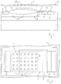
- Figure 1 shows a cross section of a high-voltage LDMOS transistor comprising a semiconductor substrate 1 with a first well 2 of a first type of conductivity and a second well 3 of the opposite second type of conductivity arranged in the first well 2.
- a source region 4 of the second type of conductivity is arranged in the first well 2 outside the second well 3
- a drain region 5 of the second type of conductivity is arranged in the second well 3
- a bulk contact region 6 of the first type of conductivity is arranged in the first well 2 outside the second well 3.
- the source region 4, the drain region 5, and the bulk contact region 6 may be provided with a source contact 14, a drain contact 15 and a body contact 16, respectively.
- the first type of conductivity may be n-type conductivity and the second type of conductivity p-type conductivity or vice versa, for the production of a p-channel LDMOS or an n-channel LDMOS, respectively.
- a gate dielectric 8 and a gate electrode 9 are arranged on a channel region, which is provided by a section of the first well 2 that is present between the second well 3 and the source region 4.
- a drift region 13 is located within the second well 3 between the source region 4 and the drain region 5.
- the drift region 13 is preferably covered with an insulation region 7, which is arranged between the drain region 5 and the gate dielectric 8 and may be a field oxide or a shallow trench isolation (STI).
- the gate electrode 9 may extend on the insulation region 7, thus forming a field plate, which modifies the electric field in the drift region 13.
- Figure 1 shows a mask 10 comprising a patterned window 11 provided with openings 12 arranged above the transistor device.
- the mask 10 is used to implant dopants of the first type of conductivity as to partially counterdope the original doping of the drift region 13 in order to produce a reduced net doping concentration in the drift region 13.
- the mask 10 is used to implant dopants of the second type of conductivity as to produce the second well 3 with a reduced doping concentration in the drift region.
- Figure 1 shows the arrangement of the patterned window 11 with respect to the transistor structure, including elements of the transistor that are not yet present when the implantation using the mask 10 is performed.
- the implantation of the second well 3 may take place using the mask 10 particularly before the formation of the source region 4, the drain region 5, the bulk contact region 6, the insulation region 7, and the gate electrode 9.
- a counterdoping using the mask 10 may take place before the formation of the source region 4, the drain region 5, the bulk contact region 6, the insulation region 7, and the gate electrode 9, for example.
- Figure 2 shows a top view of the well structure of the LDMOS transistor and of the arrangement of the patterned window 11. The corresponding elements are designated with the same reference numerals as in Figure 1.
- Figure 2 shows the relative positions of the first well 2, the second well 3 and the source region 4, which are partially covered by the gate electrode 9, the drain region 5, and the bulk contact region 6. The hidden contours are indicated with broken lines.
- the drift region 13 extends, in its longitudinal direction, from the common boundary of the second well 3 and the channel region to the drain region 5.
- the patterned window 11 comprises openings 12 which are confined in directions both along the drift region 13 and transverse to the drift region 13.
- the openings 12 are therefore substantially different from narrow strips extending along or across the drift region 13, as they may be used for transistors that are provided for operating voltages above 300 V.
- the openings 12 may be a plurality of circular or rectangular holes, for instance. Their arrangement may be symmetrical or periodical in one or more directions or may form a sieve structure. The openings 12 may be arranged at equal distances along the longitudinal extension of the drift region 13 or transverse to the drift region or at equal distances both along the drift region and transverse to the drift region. The openings are preferably sufficiently dense for the formation of a continuous drift region 13 without necessitating a subsequent annealing step. Their density may be adapted to the production of transistors that are provided for operating voltages in the range between 100 V and 300 V. The invention enables the production of high-voltage LDMOS transistors, particularly high-voltage p-channel LDMOS transistors, with conventional well implants. The patterned window is used for a local counterdoping of a previously implanted doping. The density, position and size of the openings 12 of the patterned window 11 can easily be adjusted to optimize the doping concentration of the drift region for the desired transistor types.
- the openings can be varied from smallest dimensions, according to a minimum design rule, for instance, up to dimensions in the order of micrometers, typically 0.1 to 3 ⁇ m, for example.
- the portion of the patterned window 11 that is covered by the openings 12 may vary in a wide range and may be as large as 80 % of the total area of the patterned window 11.
- Multiple windows allow the density of the openings 12 to vary locally. Areas in which the openings 12 are rather dense may be separated by intermediate areas which comprise only sparse openings or are void of openings.
- the method has the advantages that no additional mask and no additional alignment are necessary and that the implanted dose can flexibly be controlled according to the requirements of the individual embodiments of the transistor device.
Landscapes
- Insulated Gate Type Field-Effect Transistor (AREA)
Claims (6)
- Procédé de production d'un transistor LDMOS à haute tension, comprenant :- la formation d'un premier puits (2) présentant un dopage d'un premier type de conductivité dans un substrat semiconducteur (1),- la formation d'un deuxième puits (3) présentant un dopage d'un deuxième type de conductivité opposé dans le premier puits (2),- la formation d'une région de source (4) du deuxième type de conductivité dans le premier puits (2) à l'extérieur du deuxième puits (3),- la formation d'une région de drain (5) du deuxième type de conductivité dans le deuxième puits (3), laissant une région de migration (13) dans le deuxième puits (3) entre la région de drain (5) et la région de source (4),- la formation d'une région de contact de corps (6) du premier type de conductivité dans le premier puits (2), et- l'agencement d'un diélectrique de grille (8) et d'une électrode de grille (9) sur une section du premier puits (2) qui est présente entre le deuxième puits (3) et la région de source (4),sachant qu'une implantation du premier type de conductivité est effectuée dans le deuxième puits (3) dans une zone de la région de migration (13) au moyen d'un masque d'implantation (10) avec une fenêtre (11) à motif présentant des ouvertures (12) qui sont confinées dans des directions à la fois le long de la région de migration (13) et transversalement à la région de migration (13), l'implantation produisant une concentration de dopage nette réduite dans la région de migration (13).
- Procédé selon la revendication 1, sachant queles ouvertures (12) de la fenêtre (11) à motif sont adaptées pour une formation d'une région de migration (13) qui est prévue pour une tension de fonctionnement du transistor dans la plage comprise entre 100 V et 300 V.
- Procédé selon la revendication 1 ou 2, sachant queles ouvertures (12) de la fenêtre (11) à motif sont une pluralité de trous circulaires ou rectangulaires.
- Procédé selon la revendication 1 ou 2, sachant queles ouvertures (12) de la fenêtre (11) à motif forment une structure en tamis.
- Procédé selon la revendication 1 ou 2, sachant queles ouvertures (12) de la fenêtre (11) à motif sont agencées à égales distances le long de la région de migration (13) ou transversalement à la région de migration ou à la fois le long de la région de migration et transversalement à la région de migration.
- Procédé selon la revendication 1 ou 2, sachant queles ouvertures (12) de la fenêtre (11) à motif sont agencées de façon suffisamment dense pour la formation d'une région de migration (13) continue sans étape de recuit subséquente.
Priority Applications (2)
| Application Number | Priority Date | Filing Date | Title |
|---|---|---|---|
| EP12167851.0A EP2665101B1 (fr) | 2012-05-14 | 2012-05-14 | Procédé de fabrication d'un transistor LDMOS haute tension |
| PCT/EP2013/057828 WO2013171012A1 (fr) | 2012-05-14 | 2013-04-15 | Procédé de production de transistor métal oxyde semi-conducteur à diffusion latérale haute tension |
Applications Claiming Priority (1)
| Application Number | Priority Date | Filing Date | Title |
|---|---|---|---|
| EP12167851.0A EP2665101B1 (fr) | 2012-05-14 | 2012-05-14 | Procédé de fabrication d'un transistor LDMOS haute tension |
Publications (2)
| Publication Number | Publication Date |
|---|---|
| EP2665101A1 EP2665101A1 (fr) | 2013-11-20 |
| EP2665101B1 true EP2665101B1 (fr) | 2018-10-31 |
Family
ID=48142768
Family Applications (1)
| Application Number | Title | Priority Date | Filing Date |
|---|---|---|---|
| EP12167851.0A Not-in-force EP2665101B1 (fr) | 2012-05-14 | 2012-05-14 | Procédé de fabrication d'un transistor LDMOS haute tension |
Country Status (2)
| Country | Link |
|---|---|
| EP (1) | EP2665101B1 (fr) |
| WO (1) | WO2013171012A1 (fr) |
Families Citing this family (1)
| Publication number | Priority date | Publication date | Assignee | Title |
|---|---|---|---|---|
| CN107785428A (zh) * | 2016-08-30 | 2018-03-09 | 无锡华润上华科技有限公司 | 具有分离式平面场板结构的半导体器件及其制造方法 |
Family Cites Families (4)
| Publication number | Priority date | Publication date | Assignee | Title |
|---|---|---|---|---|
| US5512495A (en) | 1994-04-08 | 1996-04-30 | Texas Instruments Incorporated | Method of manufacturing extended drain resurf lateral DMOS devices |
| DE19526183C1 (de) * | 1995-07-18 | 1996-09-12 | Siemens Ag | Verfahren zur Herstellung von mindestens zwei Transistoren in einem Halbleiterkörper |
| JP2005294584A (ja) * | 2004-03-31 | 2005-10-20 | Eudyna Devices Inc | 半導体装置および不純物導入用マスクならびに半導体装置の製造方法 |
| JP4972855B2 (ja) * | 2004-08-04 | 2012-07-11 | 富士電機株式会社 | 半導体装置およびその製造方法 |
-
2012
- 2012-05-14 EP EP12167851.0A patent/EP2665101B1/fr not_active Not-in-force
-
2013
- 2013-04-15 WO PCT/EP2013/057828 patent/WO2013171012A1/fr not_active Ceased
Non-Patent Citations (1)
| Title |
|---|
| None * |
Also Published As
| Publication number | Publication date |
|---|---|
| EP2665101A1 (fr) | 2013-11-20 |
| WO2013171012A1 (fr) | 2013-11-21 |
Similar Documents
| Publication | Publication Date | Title |
|---|---|---|
| US7180132B2 (en) | Enhanced RESURF HVPMOS device with stacked hetero-doping RIM and gradual drift region | |
| US9660074B2 (en) | Methods and apparatus for LDMOS devices with cascaded RESURF implants and double buffers | |
| US7414287B2 (en) | System and method for making a LDMOS device with electrostatic discharge protection | |
| US8674442B2 (en) | Semiconductor device and manufacturing method thereof | |
| US20140065781A1 (en) | Ultra-High Voltage N-Type-Metal-Oxide-Semiconductor (UHV NMOS) Device and Methods of Manufacturing the same | |
| US11152505B2 (en) | Drain extended transistor | |
| US20080073745A1 (en) | High-voltage MOS device improvement by forming implantation regions | |
| US9105656B2 (en) | High voltage device and manufacturing method thereof | |
| CN103208519A (zh) | 与5伏cmos工艺兼容的nldmos结构及其制法 | |
| US7498652B2 (en) | Non-uniformly doped high voltage drain-extended transistor and method of manufacture thereof | |
| US20140061721A1 (en) | Mos device and method for fabricating the same | |
| US9171763B2 (en) | Methods of manufacturing a semiconductor device having varying p-top and n-grade regions | |
| EP2130218B1 (fr) | Fabrication à faible consommation de masque de transistors haute tension latéraux complémentaires à structure resurf | |
| EP2665101B1 (fr) | Procédé de fabrication d'un transistor LDMOS haute tension | |
| WO2016077803A1 (fr) | Amélioration des caractéristiques de tbj latéral dans une technologie bcd | |
| CN108417634B (zh) | 制造半导体开关装置的方法 | |
| US20150171212A1 (en) | High voltage lateral dmos transistor with optimized source-side blocking capability | |
| US9397191B2 (en) | Methods of making a self-aligned channel drift device | |
| CN102694020A (zh) | 一种半导体装置 | |
| US9722047B2 (en) | Method of producing a high-voltage transistor | |
| CN104037223A (zh) | 射频n型ldmos器件及其制造方法 | |
| TWI517295B (zh) | 具有p頂層與n能階的半導體裝置及其製造方法 | |
| CN103137623A (zh) | 一种mos型高压集成电路及制作方法 |
Legal Events
| Date | Code | Title | Description |
|---|---|---|---|
| PUAI | Public reference made under article 153(3) epc to a published international application that has entered the european phase |
Free format text: ORIGINAL CODE: 0009012 |
|
| AK | Designated contracting states |
Kind code of ref document: A1 Designated state(s): AL AT BE BG CH CY CZ DE DK EE ES FI FR GB GR HR HU IE IS IT LI LT LU LV MC MK MT NL NO PL PT RO RS SE SI SK SM TR |
|
| AX | Request for extension of the european patent |
Extension state: BA ME |
|
| 17P | Request for examination filed |
Effective date: 20140407 |
|
| RBV | Designated contracting states (corrected) |
Designated state(s): AL AT BE BG CH CY CZ DE DK EE ES FI FR GB GR HR HU IE IS IT LI LT LU LV MC MK MT NL NO PL PT RO RS SE SI SK SM TR |
|
| GRAP | Despatch of communication of intention to grant a patent |
Free format text: ORIGINAL CODE: EPIDOSNIGR1 |
|
| STAA | Information on the status of an ep patent application or granted ep patent |
Free format text: STATUS: GRANT OF PATENT IS INTENDED |
|
| INTG | Intention to grant announced |
Effective date: 20180518 |
|
| GRAS | Grant fee paid |
Free format text: ORIGINAL CODE: EPIDOSNIGR3 |
|
| GRAA | (expected) grant |
Free format text: ORIGINAL CODE: 0009210 |
|
| STAA | Information on the status of an ep patent application or granted ep patent |
Free format text: STATUS: THE PATENT HAS BEEN GRANTED |
|
| RIN1 | Information on inventor provided before grant (corrected) |
Inventor name: PARK, JONG MUN Inventor name: MINIXHOFER, RAINER |
|
| AK | Designated contracting states |
Kind code of ref document: B1 Designated state(s): AL AT BE BG CH CY CZ DE DK EE ES FI FR GB GR HR HU IE IS IT LI LT LU LV MC MK MT NL NO PL PT RO RS SE SI SK SM TR |
|
| RAP1 | Party data changed (applicant data changed or rights of an application transferred) |
Owner name: AMS AG |
|
| REG | Reference to a national code |
Ref country code: CH Ref legal event code: EP Ref country code: GB Ref legal event code: FG4D |
|
| REG | Reference to a national code |
Ref country code: AT Ref legal event code: REF Ref document number: 1060426 Country of ref document: AT Kind code of ref document: T Effective date: 20181115 |
|
| REG | Reference to a national code |
Ref country code: DE Ref legal event code: R096 Ref document number: 602012052797 Country of ref document: DE |
|
| REG | Reference to a national code |
Ref country code: IE Ref legal event code: FG4D |
|
| RAP2 | Party data changed (patent owner data changed or rights of a patent transferred) |
Owner name: AMS AG |
|
| REG | Reference to a national code |
Ref country code: NL Ref legal event code: MP Effective date: 20181031 |
|
| REG | Reference to a national code |
Ref country code: LT Ref legal event code: MG4D |
|
| REG | Reference to a national code |
Ref country code: AT Ref legal event code: MK05 Ref document number: 1060426 Country of ref document: AT Kind code of ref document: T Effective date: 20181031 |
|
| PG25 | Lapsed in a contracting state [announced via postgrant information from national office to epo] |
Ref country code: ES Free format text: LAPSE BECAUSE OF FAILURE TO SUBMIT A TRANSLATION OF THE DESCRIPTION OR TO PAY THE FEE WITHIN THE PRESCRIBED TIME-LIMIT Effective date: 20181031 Ref country code: LV Free format text: LAPSE BECAUSE OF FAILURE TO SUBMIT A TRANSLATION OF THE DESCRIPTION OR TO PAY THE FEE WITHIN THE PRESCRIBED TIME-LIMIT Effective date: 20181031 Ref country code: HR Free format text: LAPSE BECAUSE OF FAILURE TO SUBMIT A TRANSLATION OF THE DESCRIPTION OR TO PAY THE FEE WITHIN THE PRESCRIBED TIME-LIMIT Effective date: 20181031 Ref country code: NO Free format text: LAPSE BECAUSE OF FAILURE TO SUBMIT A TRANSLATION OF THE DESCRIPTION OR TO PAY THE FEE WITHIN THE PRESCRIBED TIME-LIMIT Effective date: 20190131 Ref country code: BG Free format text: LAPSE BECAUSE OF FAILURE TO SUBMIT A TRANSLATION OF THE DESCRIPTION OR TO PAY THE FEE WITHIN THE PRESCRIBED TIME-LIMIT Effective date: 20190131 Ref country code: PL Free format text: LAPSE BECAUSE OF FAILURE TO SUBMIT A TRANSLATION OF THE DESCRIPTION OR TO PAY THE FEE WITHIN THE PRESCRIBED TIME-LIMIT Effective date: 20181031 Ref country code: FI Free format text: LAPSE BECAUSE OF FAILURE TO SUBMIT A TRANSLATION OF THE DESCRIPTION OR TO PAY THE FEE WITHIN THE PRESCRIBED TIME-LIMIT Effective date: 20181031 Ref country code: LT Free format text: LAPSE BECAUSE OF FAILURE TO SUBMIT A TRANSLATION OF THE DESCRIPTION OR TO PAY THE FEE WITHIN THE PRESCRIBED TIME-LIMIT Effective date: 20181031 Ref country code: IS Free format text: LAPSE BECAUSE OF FAILURE TO SUBMIT A TRANSLATION OF THE DESCRIPTION OR TO PAY THE FEE WITHIN THE PRESCRIBED TIME-LIMIT Effective date: 20190228 Ref country code: AT Free format text: LAPSE BECAUSE OF FAILURE TO SUBMIT A TRANSLATION OF THE DESCRIPTION OR TO PAY THE FEE WITHIN THE PRESCRIBED TIME-LIMIT Effective date: 20181031 |
|
| PG25 | Lapsed in a contracting state [announced via postgrant information from national office to epo] |
Ref country code: SE Free format text: LAPSE BECAUSE OF FAILURE TO SUBMIT A TRANSLATION OF THE DESCRIPTION OR TO PAY THE FEE WITHIN THE PRESCRIBED TIME-LIMIT Effective date: 20181031 Ref country code: GR Free format text: LAPSE BECAUSE OF FAILURE TO SUBMIT A TRANSLATION OF THE DESCRIPTION OR TO PAY THE FEE WITHIN THE PRESCRIBED TIME-LIMIT Effective date: 20190201 Ref country code: AL Free format text: LAPSE BECAUSE OF FAILURE TO SUBMIT A TRANSLATION OF THE DESCRIPTION OR TO PAY THE FEE WITHIN THE PRESCRIBED TIME-LIMIT Effective date: 20181031 Ref country code: NL Free format text: LAPSE BECAUSE OF FAILURE TO SUBMIT A TRANSLATION OF THE DESCRIPTION OR TO PAY THE FEE WITHIN THE PRESCRIBED TIME-LIMIT Effective date: 20181031 Ref country code: RS Free format text: LAPSE BECAUSE OF FAILURE TO SUBMIT A TRANSLATION OF THE DESCRIPTION OR TO PAY THE FEE WITHIN THE PRESCRIBED TIME-LIMIT Effective date: 20181031 Ref country code: PT Free format text: LAPSE BECAUSE OF FAILURE TO SUBMIT A TRANSLATION OF THE DESCRIPTION OR TO PAY THE FEE WITHIN THE PRESCRIBED TIME-LIMIT Effective date: 20190301 |
|
| PG25 | Lapsed in a contracting state [announced via postgrant information from national office to epo] |
Ref country code: CZ Free format text: LAPSE BECAUSE OF FAILURE TO SUBMIT A TRANSLATION OF THE DESCRIPTION OR TO PAY THE FEE WITHIN THE PRESCRIBED TIME-LIMIT Effective date: 20181031 Ref country code: IT Free format text: LAPSE BECAUSE OF FAILURE TO SUBMIT A TRANSLATION OF THE DESCRIPTION OR TO PAY THE FEE WITHIN THE PRESCRIBED TIME-LIMIT Effective date: 20181031 Ref country code: DK Free format text: LAPSE BECAUSE OF FAILURE TO SUBMIT A TRANSLATION OF THE DESCRIPTION OR TO PAY THE FEE WITHIN THE PRESCRIBED TIME-LIMIT Effective date: 20181031 |
|
| REG | Reference to a national code |
Ref country code: DE Ref legal event code: R097 Ref document number: 602012052797 Country of ref document: DE |
|
| PG25 | Lapsed in a contracting state [announced via postgrant information from national office to epo] |
Ref country code: SM Free format text: LAPSE BECAUSE OF FAILURE TO SUBMIT A TRANSLATION OF THE DESCRIPTION OR TO PAY THE FEE WITHIN THE PRESCRIBED TIME-LIMIT Effective date: 20181031 Ref country code: SK Free format text: LAPSE BECAUSE OF FAILURE TO SUBMIT A TRANSLATION OF THE DESCRIPTION OR TO PAY THE FEE WITHIN THE PRESCRIBED TIME-LIMIT Effective date: 20181031 Ref country code: RO Free format text: LAPSE BECAUSE OF FAILURE TO SUBMIT A TRANSLATION OF THE DESCRIPTION OR TO PAY THE FEE WITHIN THE PRESCRIBED TIME-LIMIT Effective date: 20181031 Ref country code: EE Free format text: LAPSE BECAUSE OF FAILURE TO SUBMIT A TRANSLATION OF THE DESCRIPTION OR TO PAY THE FEE WITHIN THE PRESCRIBED TIME-LIMIT Effective date: 20181031 |
|
| PLBE | No opposition filed within time limit |
Free format text: ORIGINAL CODE: 0009261 |
|
| STAA | Information on the status of an ep patent application or granted ep patent |
Free format text: STATUS: NO OPPOSITION FILED WITHIN TIME LIMIT |
|
| 26N | No opposition filed |
Effective date: 20190801 |
|
| PG25 | Lapsed in a contracting state [announced via postgrant information from national office to epo] |
Ref country code: SI Free format text: LAPSE BECAUSE OF FAILURE TO SUBMIT A TRANSLATION OF THE DESCRIPTION OR TO PAY THE FEE WITHIN THE PRESCRIBED TIME-LIMIT Effective date: 20181031 |
|
| REG | Reference to a national code |
Ref country code: CH Ref legal event code: PL |
|
| PG25 | Lapsed in a contracting state [announced via postgrant information from national office to epo] |
Ref country code: MC Free format text: LAPSE BECAUSE OF FAILURE TO SUBMIT A TRANSLATION OF THE DESCRIPTION OR TO PAY THE FEE WITHIN THE PRESCRIBED TIME-LIMIT Effective date: 20181031 Ref country code: LI Free format text: LAPSE BECAUSE OF NON-PAYMENT OF DUE FEES Effective date: 20190531 Ref country code: CH Free format text: LAPSE BECAUSE OF NON-PAYMENT OF DUE FEES Effective date: 20190531 |
|
| REG | Reference to a national code |
Ref country code: BE Ref legal event code: MM Effective date: 20190531 |
|
| PG25 | Lapsed in a contracting state [announced via postgrant information from national office to epo] |
Ref country code: LU Free format text: LAPSE BECAUSE OF NON-PAYMENT OF DUE FEES Effective date: 20190514 |
|
| PG25 | Lapsed in a contracting state [announced via postgrant information from national office to epo] |
Ref country code: TR Free format text: LAPSE BECAUSE OF FAILURE TO SUBMIT A TRANSLATION OF THE DESCRIPTION OR TO PAY THE FEE WITHIN THE PRESCRIBED TIME-LIMIT Effective date: 20181031 |
|
| PG25 | Lapsed in a contracting state [announced via postgrant information from national office to epo] |
Ref country code: IE Free format text: LAPSE BECAUSE OF NON-PAYMENT OF DUE FEES Effective date: 20190514 |
|
| PG25 | Lapsed in a contracting state [announced via postgrant information from national office to epo] |
Ref country code: BE Free format text: LAPSE BECAUSE OF NON-PAYMENT OF DUE FEES Effective date: 20190531 |
|
| PGFP | Annual fee paid to national office [announced via postgrant information from national office to epo] |
Ref country code: FR Payment date: 20200522 Year of fee payment: 9 Ref country code: DE Payment date: 20200520 Year of fee payment: 9 |
|
| PGFP | Annual fee paid to national office [announced via postgrant information from national office to epo] |
Ref country code: GB Payment date: 20200603 Year of fee payment: 9 |
|
| PG25 | Lapsed in a contracting state [announced via postgrant information from national office to epo] |
Ref country code: CY Free format text: LAPSE BECAUSE OF FAILURE TO SUBMIT A TRANSLATION OF THE DESCRIPTION OR TO PAY THE FEE WITHIN THE PRESCRIBED TIME-LIMIT Effective date: 20181031 |
|
| PG25 | Lapsed in a contracting state [announced via postgrant information from national office to epo] |
Ref country code: HU Free format text: LAPSE BECAUSE OF FAILURE TO SUBMIT A TRANSLATION OF THE DESCRIPTION OR TO PAY THE FEE WITHIN THE PRESCRIBED TIME-LIMIT; INVALID AB INITIO Effective date: 20120514 Ref country code: MT Free format text: LAPSE BECAUSE OF FAILURE TO SUBMIT A TRANSLATION OF THE DESCRIPTION OR TO PAY THE FEE WITHIN THE PRESCRIBED TIME-LIMIT Effective date: 20181031 |
|
| REG | Reference to a national code |
Ref country code: DE Ref legal event code: R119 Ref document number: 602012052797 Country of ref document: DE |
|
| GBPC | Gb: european patent ceased through non-payment of renewal fee |
Effective date: 20210514 |
|
| PG25 | Lapsed in a contracting state [announced via postgrant information from national office to epo] |
Ref country code: GB Free format text: LAPSE BECAUSE OF NON-PAYMENT OF DUE FEES Effective date: 20210514 Ref country code: DE Free format text: LAPSE BECAUSE OF NON-PAYMENT OF DUE FEES Effective date: 20211201 |
|
| PG25 | Lapsed in a contracting state [announced via postgrant information from national office to epo] |
Ref country code: FR Free format text: LAPSE BECAUSE OF NON-PAYMENT OF DUE FEES Effective date: 20210531 |
|
| PG25 | Lapsed in a contracting state [announced via postgrant information from national office to epo] |
Ref country code: MK Free format text: LAPSE BECAUSE OF FAILURE TO SUBMIT A TRANSLATION OF THE DESCRIPTION OR TO PAY THE FEE WITHIN THE PRESCRIBED TIME-LIMIT Effective date: 20181031 |